3D IC Packaging 3D IC Integration. John H. Lau ASM Pacific Technology Kung Yip Street, Kwai Chung, Hong Kong ,
|
|
|
- Damon Gregory
- 5 years ago
- Views:
Transcription
1 3D IC Packaging 3D IC Integration John H. Lau ASM Pacific Technology Kung Yip Street, Kwai Chung, Hong Kong , CPMT Distinguish Lecture, San Diego Chapter, February 23,
2 Contents 3D IC Packaging (without TSV) Stack Chips by Wire Bonding Package-on-Package (PoP) Chip-to-Chip Interconnects Embedded Fan-Out Wafer Level Package (ewlp) Infineon, Freescale, TSMC s ewlp Infineon, ASE, Amkor, STATSchippac, STMicroelectroinc s 3D ewlp 3D IC Integration Memory-Chip Stacking in Production Hybrid Memory Cube (HMC) Intel s Knight s Landing with HMC Fujitsu s Supercomputer with HMC Altera s FPGA with HMC Wide I/O DRAM and Wide I/O 2 High Bandwidth Memory (HBM) Samsung s Widcon Technology for Mobile Products 2.5D IC Integration Xilinx/TSMC s Interposer Altera/TSMC s Interposer ITRI s Interposer for 3D IC Integration Supply Chains and Ownerships for 2.5D/3D IC Integration Recent Advances in Package Substrates Coreless Substrates Thin-Film Layer on Build-up Package Substrate Embedded Interposer/Bridge 3D MEMS and IC Integration 3D CIS and IC Integration Summary and Q&A 2
3 Maturity 3D Integration Technologies Don t use TSV Use TSV technology 3D IC Packaging 3D IC Integration 3D Si Integration Mass Production Full swing production for memories. Volume production for mobile products. Commercia -lization Applied R&D Basic/ Applied R&D Die Stacking with wire bonds Package on Package (PoP) Stacking C2C, C2W, W2W Stacking Active applied R&D is undertaken by Research Institutes. TSV cost is the key. In the phase of industrialization. Still in upstream research, technological challenges such as KGD, yield & device architecture and EDA are key issues. W2W Stacking Technology 3 Lau, IEEE-ECTC PDC, 2009
4 3D IC Packaging (No TSV) Memory Stacked with Wirebonds Solder Bumped Flip Chip Assembly Package-on-Package (PoP) Chip-to-Chip Interconnects Embedded Fan-Out Wafer Level Package (ewlp) 4
5 Memory Stacked with Wirebonds 5
![Memory chips stacking by die attach and wire bonding [1994, nchip] Memory](/docs-images/88/115674140/images/6-0.jpg "chips Die attach material Substrate Chip 3 Chip 2 Chip 1 Bevel or Notch Bond")
6 Memory chips stacking by die attach and wire bonding [1994, nchip] Memory chips Die attach material Substrate Chip 3 Chip 2 Chip 1 Bevel or Notch Bond wires 6
 8GB (Gigabyte)")
")
7 Samsung s Eight-Stack Flash in Apple s iphone 4s SK Hynix s MLC (Multi Level Cell) 8GB (Gigabyte) NAND Flash in Apple s iphone 5s Wire bonding Nand Flash chips FBGA (Fine-pitch Ball Grid Array) Molding 7

8 Amkor s 3D IC Packaging with Cu Wires Top Chip Cu Wires Bottom Chip Substrate 8
9 Package-on-Package (PoP) 9
10 PoP (Package-on-Package) Format (Apple A7 Application Processor Chipset) Apple s A7 processor Elpida s 1GB LPDDR Build-up package substrate 10
11 Top-View and Cross Section View of the PoP (for Mobile DRAM and A8 Processor) inside iphone 6 Plus Top-side of the bottom PoP (426-ball) Elpida s 1GB LPDDR3 (EDF8164A3PM-GD-F) Application Processor Package Substrate for LPDDR3 Package Substrate for A8 processor Not-to-scale Apple s application processor (POXY99001)

12 Top-View and Cross Section View of the PoP (for Mobile DRAM and Application Processor) iphone 6 Plus iphone 6S Elpida s 1GB LPDDR3 (EDF8164A3PM-GD-F) 2GB LPDDR4 Package Substrate for LPDDR3 Package Substrate for LPDDR4 Package Substrate for A8 processor Package Substrate for A9 processor A8 application processor fabricated by 20nm process Not-to-scale A9 application processor fabricated by 14/16nm Fin-FET process
 epop Exynos Microprocessor A 40% PCB saving!")
13 Samsung s Next Generation High-End Smartphones LPDDR3 Exynos Microprocessor Conventional Solution Flash chip-set PCB epop Solution epop (Flash and LPDDR3 combination) epop Exynos Microprocessor A 40% PCB saving! PCB
14 Chip-to-Chip Interconnects 14
15 IME s Stacked Silicon Module Attached on a Substrate Heat spreader/sink (optional) Microbump Mother Chip Daughter Chip Solder Bump Rigid or Flex Substrate Solder Ball PCB Chip-to-Chip and Face-to-Face Lim, Lau, et.al., Process Development and Reliability of Microbumps, IEEE/EPTC, 2008, pp Also, IEEE Transactions on CPMT, 2010, pp
 Solder bumps Wire")


16 SONY's CXD53135GG used a 5-chip stack. (Wire bonding and solder bump) Solder bumps Wire bonds Face-to-face (Chip-to-chip) Processor: 250μm. All the other chips: Samsung 2-Gb mobile DDR2 SDRAMs 100 to 125μm a spacer die Samsung 2-Gb mobile DDR2 SDRAMs Samsung 1-Gb wide I/O SDRAM Processor 16
. The mother die is then flip chip mounted onto a substrate Cu Pillar Micro-bumps Daughter Die 17")
17 Amkor s POSSUM assembly where the daughter die (e.g., memory) is mounted face-to-face with the larger mother die (e.g., SoC). The mother die is then flip chip mounted onto a substrate Cu Pillar Micro-bumps Daughter Die 17


18 Amkor s Double POSSUM multi-stacked die configurations without the use of TSVs Daughter Die Grandma Die PCB Package Substrate Cu Pillar Micro-bumps with SnAg solder caps Mother Die SnAg Cu Sutanto, J., POSSUM TM, Die Design as a Low Cost 3D Packaging Alternative, 3D Packaging, Issue No. 25, November 2012, pp

19 Amkor s POSSUM Package showing Altera s FPGA and ASIC Package Substrate FPGA 40μm-pitch Cu-pillar + solder cap microbumps ASIC 200μm-pitch Cupost + solder Solder balls Heat spreader cap FPGA Package Substrate Solder balls ASIC Heat spreader cap FPGA Package Substrate ASIC Lau Package Substrate FPGA ASIC 40μm-pitch Cu-pillar + solder cap microbumps 200μm-pitch Cupost + solder Xie, J., and D. Patterson, Realizing 3D IC Integration with Face-to-Face Stacking, Chip Scale Review, May-June Issue, 2013, 19 pp
20 Embedded Fan-Out Wafer Level Package (ewlp) 20
 Molded reconfigured wafer Fan-Out")


21 Infineon s Embedded Wafer-Level Test for KGD Ball Grid Array (ewlb) Molded reconfigured wafer Fan-Out Area (Mold) Chip Redistribution Layer (RDL) Schematic process flow for a fan-out wafer-level package Brunnbauer, et.al., An Embedded Device Technology Based on a Molded Reconfigured Wafer, IEEE/ECTC, 2006, pp

22 a) Laminate Carrier, b) Pick and Place, c) Molding, d) Release Tape, and e) Peal Tape 2-side tape Carrier Chip face-down Molding Infineon picked a modified, commercially available tape, which is equipped with a thermorelease layer. It is loosing its adhesive properties once it is heated above a specific temperature, which is higher than any processing temperature before. Peal tape ECTC
.")
, Samsung (baseband modem), and Nokia (baseband modem and RF transceiver) have used Infineon s ewlb in their cell phone products.")
23 Infineon was the First Company to Commercialize its own ewlb Packaging Technology in an LGE cell-phone in early 2009 Mold Baseband SoC PCB RDLs Solder ball Infineon s chip is a wireless baseband SoC with multiple integrated functions (GPS, FM radio, BT ). The same ewlb product has also been in production in Nokia handsets since LGE (wireless baseband), Samsung (baseband modem), and Nokia (baseband modem and RF transceiver) have used Infineon s ewlb in their cell phone products. Infineon ewlb (wireless operation acquired by Intel in 2011) Intel RF IC 5 mm x 5 mm x 0.67 mm with 139 I/Os and 0.4mm ball pitch Intel LTE analog baseband 23


24 Freescale s Redistributed Chip Package (RCP) Place die active side down on substrate and encapsulated with a silica-filled epoxy molding compound Remove substrate and turn the whole around Redistribute signal, power and ground 200mm RCP panel with 82 17mmx17mm 208 I/O packages Deposit BGA solder balls Saw panel into individual package A 208 I/O 13mmx13mm PBGA with 0.65mm pitch can be shrunk to a 9mmx9mm RCP with 0.5mm pitch Keser, et.al., The Redistributed Chip Package: A Breakthrough for Advanced Packaging, IEEE/ECTC, 2007, pp

 Solder")
25 Fan-Out ewlp (Embedded Wafer-Level Packaging) Solder balls Pads RDLs KGD 25
26 Embedded Fan-Out Wafer Level Package (ewlp) vs. PBGA (Plastic Ball Grid Array) Fan-out area (Molded Compound) Face-down Chip Redistribution layer (RDL) Solder Balls Underfill Molded Compound Face-down Chip Substrate Solder Balls Solder Bumps Eliminate solder bumps, underfill, and package substrate. Lower Profile! 26
27 Companies who are Manufacturing/Working on ewlp Infineon s Embedded Wafer-Level Ball Grid Array (ewlb) Package licensed by ASE, STATS ChipPAC, NANIUM, STMicroelectronics Freescale s Redistributed Chip Package (RCP) licensed by NEPES TSMC s Integrated Fan-Out Wafer-Level Package (InFO-WLP) ASE s 3D Fan-Out Wafer-Level PoP (FOPOP) AMKOR s Wafer-Level Fan-Out (WLFO) Package SPIL s Panel Fan-out (P-FO) Package STATSChipPAC s Embedded Wafer Level PoP (ewlb-pop) PTI (NEPES) Fan-Out Wafer-Level Package (FOWLP (RCP)) J-DEVICES Wafer-Level Fan-Out Package (WFOP) ADL Engineering s Panel Wafer-Level BGA Package (pwlp) STMicroelectronics Embedded Wafer Level LGA (ewll) NANIUM s Fan-Out Wafer-Level Package (FO-WLP) DECA s Fan-Out Wafer-Level Packaging (FOWLP) Embedded Fan-Out Wafer-Level Package (ewlp) 27

28 TSMC InFO-WLP (Integrated Fan-Out WLP) At the TSMC Technology Symposium in San Jose, CA in April 2014, TSMC announced the latest InFO-WLP platforms: 8mm x 8mm is targeted at RF and WiFi chips 15mm x 15mm is targeted at application processor and baseband chips 25mm x 25mm could be applied to GPU and networking chips 28

29 High-Performance Integrated Fan-Out Wafer Level Packaging (InFO-WLP): Technology and System Integration Christianto C. Liu, Shuo-Mao Chen, Feng-Wei Kuo, Huan-Neng Chen, En-Hsiang Yeh, Cheng-Chieh Hsieh, Li-Hsien Huang, Ming-Yen Chiu, John Yeh, Tsung-Shu Lin, Tzu-Jin Yeh, Shang-Yun Hou, Jui-Pin Hung, Jing-Cheng Lin, Chewn-Pu Jou, Chuei-Tang Wang, Shin-Puu Jeng, Douglas C.H. Yu Taiwan Semiconductor Manufacturing Company, Ltd., Hsinchu, Taiwan, chris IEEE/IEDM2012
 Baseband Processor PBGA Baseband Processor InFO-WLP")
30 Transceiver Transceiver Thermal Management between PBGA and InFO-WLP of Baseband Chip Set (TSMC Results) Baseband Processor PBGA Baseband Processor InFO-WLP Not-to-Scale


31 Thermal Result between PBGA and InFO-WLP PBGA Max. Tem = 90.5 o C Thermal resistant = 32.5 o C/W InFO-WLP Max. Tem = 81.5 o C Thermal resistant = 28.0 o C/W First, omission of the substrate layer in InFO-WLP reduces both form factor and chip-to-board thermal path, the latter especially vital in applications without heat sinks where heat primarily travels towards the board. Second, junction-to-ambient thermal path is reduced with InFO- WLP s more efficient multi-chip packaging. Third, reduced die separation in InFO-WLP improves lateral heat spreading, as shown by the more uniform heat distribution among the dies. Overall, thermal resistance of InFO-WLP technology is about 14% better than conventional MCM (28.0 versus 32.5 o C/W). Here, the difference in thermal resistance translates to a 9.0 o C reduction in maximum temperature.
32 3D ewlb Horizontal and Vertical Interconnects for Integration of Passive Components M. Wojnowski1, G. Sommer1, K. Pressel2, G. Beer2 1Infineon Technologies AG, Am Campeon 1-12, Neubiberg, Germany 2Infineon Technologies AG, Wernerwerkstraße 2, Regensburg, Germany Chip Through Encapsulant Via (TEV) Mold Compound RDLs Chip 32 IEEE/ECTC2013
 Mold Compound RDLs")
33 3D IC Packaging: PoP Chip Through Encapsulant Via (TEV) Mold Compound RDLs Chip 33
 Sputter the Ti/Cu + Cu")
34 Through Encapsulant Via (TEV) Laser Drilled Through Encapsulant Via ( µm) Sputter the Ti/Cu + Cu plating 34


35 STMicroelectronics 3D ewlb Chip 1 Chip 2 Chip 3 Chip 1 Chip 2 35
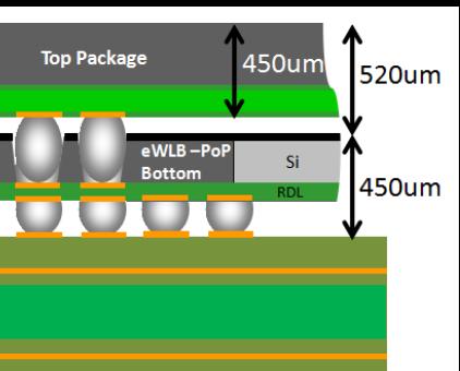
 RDLs MC Chip Top")

36 ASE s Double Sided 3D FOWLP Package on Package (FOPOP) RDLs MC Chip Top Package Through Mold Via Chip MC Bottom Package RDLs SEMICON West


37 AMKOR s Wafer-Level Fan-Out (WLFO) Package Wire Bonds Memory Chips Chip Solder Bump Redistribution Layers Substrate Through Mold Vias 3D Packaging, November

38 STATSChipPac s 3D IC Packaging 38
39 Maturity 3D Integration Technologies Don t use TSV Use TSV technology 3D IC Packaging 3D IC Integration 3D Si Integration Mass Production Full swing production for memories. Volume production for mobile products. Commercia -lization Applied R&D Basic/ Applied R&D Die Stacking with wire bonds Package on Package (PoP) Stacking C2C, C2W, W2W Stacking Active applied R&D is undertaken by Research Institutes. TSV cost is the key. In the phase of industrialization. Still in upstream research, technological challenges such as KGD, yield & device architecture and EDA are key issues. W2W Stacking Technology 39 Lau, IEEE-ECTC PDC, 2009
40 TSV (Through-Silicon Via) 40
 on July 17, 1962.")
41 TSV (Through-Silicon Via) William Shockley (co-invented the transistor) filed a patent, Semiconductive Wafer and Method of Making the Same on October 23, 1958 and was granted the US patent (3,044,909) on July 17, William Shockley (1956 Nobel laureate) Deep Pits (Holes), We call TSV today 41

42 Intel s TSV (Through-Silicon Via) for the Shortest Chip-to-Chip Interconnects A four stack wire-bonded die package Wirebonds Wirebonds are replaced by TSVs Wire TSV Microbumps Thin chips Advantages: Smaller formfactor Low power consumption Wider bandwidth Better performance 42 Lau, Reliability of 3D IC Interconnects, 2011
43 3D IC Integration Memory chip stacking Wide I/O DRAM, Wide I/O 2, or Hybrid Memory Cube (HMC) High Bandwidth Memory (HBM) 43
 Said the 1965 Nobel Physics laureate, Richard Feynman at the Gakushuin University (Tokyo) in 1985: Another direction of improvement (of computing power) is to make physical machines three")
44 3D IC Integration (The right thing to do!) Said the 1965 Nobel Physics laureate, Richard Feynman at the Gakushuin University (Tokyo) in 1985: Another direction of improvement (of computing power) is to make physical machines three dimensional instead of all on a surface of a chip (2D). That can be done in stages instead of all at once you can have several layers and then add many more layers as time goes on. Thin Chip TSV Micro Bumps 44
45 3D IC Integration (The right thing to do!) Thin Chip TSV Micro Bumps TSVs straight through the same memory chips to: enlarge the memory capacity lower the power consumption increase the bandwidth lower the latency (enhance electrical performance) reduce the form factor will be the major applications of 3D IC Integration! 45
46 Potential Applications of 3D IC Integration Memory-Chip Stacking DRAM or NAND Flash stacking with TSVs on organic substrate Over molding the DRAMs or NAND Flash Wide I/O DRAM (Hybrid Memory Cube) DRAM stacking with TSVs on Logic Controller with TSVs Over molding the DRAMs Wide I/O Interface (2.5D IC Integration) TSV-less chips on a device-less wafer (interposer) with TSVs Underfill is needed between chips and the interposer Organic Package Substrate PCB Underfill is needed between the active/passive TSV interposer and the organic substrate 46
47 Memory chip stacking 47
 560μm TSV Micro bump Thin")
 connected with TSV and microbumps 720μm 560μm")
48 Samsung s 3D Stacking with TSV (Through Silicon Via) 16Gb Flash memory (8 x 2Gb) 560μm TSV Micro bump Thin Chip Wafer before back-grinding 8-stack chips (50μm each) connected with TSV and microbumps 720μm 560μm 48
 Server Farm The 64GB DDR4 DRAM module consists of 36 DDR4")


49 Samsung Mass-Produces Industry's First TSV-based DDR4 DRAM (August 27, 2014) Server Farm The 64GB DDR4 DRAM module consists of 36 DDR4 DRAM chips, each of which consists of four 4-gigabit (Gb) DDR4 DRAM dies. Use Samsung s 20nm process technology and 3D TSV packaging technology. Perform twice as fast as a module that uses wire bonding packaging, while consuming approximately half the power. Samsung 49
50 Potential Applications of 3D IC Integration Memory-Chip Stacking DRAM or NAND Flash stacking with TSVs on organic substrate Over molding the DRAMs or NAND Flash Wide I/O DRAM (Hybrid Memory Cube) DRAM stacking with TSVs on Logic Controller with TSVs Over molding the DRAMs Wide I/O Interface (2.5D IC Integration) TSV-less chips on a device-less wafer (interposer) with TSVs Underfill is needed between chips and the interposer Organic Package Substrate PCB Underfill is needed between the active/passive TSV interposer and the organic substrate 50
51 Hybrid Memory Cube (HMC) 51

52 Hybrid Memory Cube (HMC) Over-Mold Underfill Microbump TSV TSV Organic Substrate DRAMs Logic Controller
 Logic Controller The SPEC was")

53 Hybrid Memory Cube (HMC) The HMC consortium already has 8 members: Micron Samsung Altera ARM IBM Open-Silicon SK Hynix Xilinx DRAM Layers (Memory cube) Logic Controller The SPEC was published on April 2, 2013 and is primarily targeted at: HPC (high performance computing) Networking Energy, Wireless communications Transportation Security High-end servers More than 120 adopters! 53
 DRAMs that sit on top.")
54 Hybrid Memory Cube (HMC) Architecture Each DRAM die is divided into 16 "cores" and then stacked. The logic base is at the bottom, with 16 different logic segments, each segment controlling four (or eight) DRAMs that sit on top. This type of memory architecture supports more DRAM I/O pins and, therefore, more bandwidth (as high as 400GB/s). According to the Hybrid Memory Cube Consortium, a single HMC can deliver more than 15X the performance of a DDR3 module and consume 70% less energy per bit than DDR TSVs on each DRAM 54

55 55
")

56 Hybrid Memory Cube DRAM Layers (Memory cube) Micron fabricate the memory cube Logic Controller 56

57 Hybrid Memory Cube DRAM Layers (Memory cube) Logic Controller IBM fabricate the Logic Controller 57
58 Micron s First HMC Sample Shipped in the Last Week of September 2013 DRAM Stack Package Substrate The hybrid memory cube is a 4- DRAM (each one with TSVs) on a logic controller (which size is slightly larger than the DRAMs) with TSVs The hybrid memory cube is on an organic package substrate. The TSV-DRAM is ~50-μm thick. The TSV-DRAM is with 20-μm (tall) Cu pillar + solder cap. The memory cube is assembled one DRAM at a time with thermal compression bonding. The heat dissipation is from 10W to 20W. TSV diameter ~ 5 to 6-μm. Volume production will be in next summer. 58
59 Altera s Stratix V FPGA with Micron HMC Stratix V FPGA 10/100/1000 Ethernet Connectors ATX Form Factor Hybrid Memory Cube (HMC) ATX Power Supply Connector By providing equivalent bandwidth of greater than eight (8) DDR DIMMs using a single HMC device. Altera White Paper, Addressing Next-Generation Memory Requirements Using Altera FPGAs and HMC Technology, Altera Corporation, January
 5X the bandwidth vs.")
60 Rik Myslewski, Intel teams with Micron on next-gen many-core Xeon Phi with 3D DRAM Introduces new 'fundamental building 60 block of HPC systems' with Intel Omni Scale Fabric, Posted in HPC, June Intel s Knight s Landing with 8 HMC Fabricated by Micron (2015 production) 5X the bandwidth vs. GDDR5 Up to 16GB One-third the footprint Half the energy per bit Managed memory stack for optimal levels of reliability, availability and serviceability Hybrid Memory Cube (HMC)
 32 + 2 core CPU Hybrid Memory Cube (HMC)")

61 Fujitsu s Tofu2 integrated Components: SPARC64 Xifx and CPU Memory Board Three CPUs 3 x 8 Hybrid Memory Cubes (HMCs) core CPU Hybrid Memory Cube (HMC) SPARC64 Xifx CPU Memory Board Yoshida, SPARC64 Xifx: Fujitsu s next generation processor for HPC, Hot Chips: A Symposium on High Performance Chips, August 11,
62 Wide I/O DRAM 62


63 Wide I/O Single Date Rate JEDEC Standard (JESD229), December 2011 Target: 1mm Micron s Suggestion Target: 10mmx10mm Max. The minimum determined by contact grid TSVs Contact Grid TSVs Face-down Face-up Memory Cube with TSVs SoC with TSVs Solder Balls (a) C4 Bumps (b) 63
64 Wide I/O 2 64
65 JEDEC Standard - Wide I/O 2 (JESD229-2, Wide I/O 2, August 29, 2014) 40µm 40µm 2880µm 1000µm 120µm 200µm
66 HIGH Bandwidth Memory (HBM) 66

67 High Bandwidth Memory (HBM) DRAM (Mainly for Graphic applications) JEDEC Standard (JESD235), October 2013 HBM is designed to support bandwidth from 128GB/s to 256GB/s Hynix s HMC TSV/RDL Interposer GPU/CPU/SoC TSV HBM Interface HBM DRAM Optional Base Chip Organic Package Substrate PCB PCB Underfill is needed between the interposer and the organic substrate. Also, underfill is needed between the interposer and the GPU/CPU and the memory cube 67
68 Memory Stacking with TSVs Memory Structure Bandwidth (GBps) Voltage (V) Standard Applications RDIMMs DDR4 Servers, Cloud, data center, etc. Wide IO JESD229-2 High-end smartphones HMC 160 to HMC SPEC High-end servers, networking, graphics, HPC, FPGA, etc. HBM 128 to JESD235 High-end graphics, networking, HPC, etc.
69 Samsung s Widcon (wide I/O connection) Technology 69
 Elpida s 1GB LPDDR3")

70 Top-View and Cross Section View of the PoP (for Mobile DRAM and A8 Processor) inside iphone 6 Plus Top-side of the bottom PoP (426-ball) Elpida s 1GB LPDDR3 (EDF8164A3PM-GD-F) Application Processor Package Substrate for LPDDR3 Package Substrate for A8 processor Not-to-scale Apple s application processor (POXY99001)
71 Mobile Application Processor (AP) Chip Set (AP + LPDDR3) (PoP vs. 3D IC Integration) Wide I/O DRAMs PoP 3D IC Integration Microbump TSV Wide I/O DRAMs Package Substrate for LPDDR3 AP AP Package Substrate for AP Package Substrate for AP Chip Set Samsung s Widcon Technology Very low profile Widest memory bandwidth Lower power consumption

72 Samsung s Widcon Technology vs. PoP

73 Samsung s Widcon Technology vs. PoP
74 2.5D IC Integration 74
75 Potential Applications of 3D IC Integration Memory-Chip Stacking DRAM or NAND Flash stacking with TSVs on organic substrate Over molding the DRAMs or NAND Flash Wide I/O DRAM (Hybrid Memory Cube) DRAM stacking with TSVs on Logic Controller with TSVs Over molding the DRAMs Wide I/O Interface (2.5D IC Integration) TSV-less chips on a device-less wafer (interposer) with TSVs Underfill is needed between chips and the interposer Organic Package Substrate PCB Underfill is needed between the active/passive TSV interposer and the organic substrate 75

76 On October 21, 2013 Xilinx and TSMC have jointly announced production release of the Virtex-7 HT family, what the pair claims is the industry's first heterogeneous 3D ICs in production. 2FPGAs TSV/RDL Interposer Transceiver Organic Package Substrate The Xilinx Virtex-7 HT FPGAs feature up to sixteen, 28Gbps and seventy-two, 13.1Gbps transceivers. In addition to the Virtex-7 HT FPGAs, two other homogeneous devices in the 3D IC family have been in volume production since early 2013 Virtex T and Virtex-7 X1140T series. 4 FPGAs TSV/RDL Interposer Organic Package Substrate 76


77 Xilinx/TSMC s 2.5D IC Integration with FPGA PTH Build-up Layers Chip Core Package Substrate Chip Interposer C4 Bumps Devices (Cannot see) Metal Layers Metal Contacts Si Solder Balls Micro Bump Cu Pillar Solder 4RDLs Interposer TSV The package substrate is at least (5-2-5) RDLs: 0.4μm-pitch line width and spacing Each FPGA has >50,000 μbumps on 45μm pitch Interposer is supporting >200,000 μbumps 77

, a very large SoC has been sliced")

78 Xilinx s Passive Interposers with TSV and RDL for Wide I/O Interface in FPGA Products For better manufacturing yield (to save cost), a very large SoC has been sliced into 4 smaller chips (2011) (10,000+) With 4 RDLs Lau 78 Lau, IEEE/ECTC2011 3D IC Integration PDC


79 Altera/TSMC s 2.5D IC Integration with FPGA Interposer C4 Bumps Chip Build-up Layers Package Substrate Solder Cu Pillar Solder Balls The package substrate is at least (6-2-6) Interposer TSV RDLs 4RDLs on top of the interposer and there isn t any at the bottom 79
80 2.5D IC Integration (Interposers) Underfill UBM Cu Pillar Chip 1 Chip 2 Solder RDLs (Redistribution layers) Underfill TSV RDLs for lateral communications Si Interposer UBM Solder Bumps Package Substrate Build-up Layers Solder Balls Not-to-scale 80
81 Thus, passive TSV/RDL interposers are for extremely finepitch, high-i/o, high-performance, and high-density semiconductor IC applications. 81
82 Recent Advances in Package substrates Coreless Substrates Build-Up Package Substrates
83 Coreless Substrates 83


84 Comparison between the Substrate with Build-up Layers and Coreless Substrate Conventional Build-up Package substrate Chip Underfill Bump Build-up Layers Core Build-up Layers Filled Micro Via Coreless Package substrate Chip Underfil Bump l Build-up Layers Layers Filled Micro Via Low Profile: Good for mobile products 84
85 Coreless Substrates Advantages Lower cost by eliminating the core Better electrical performance (good high-speed transmission characteristic) Higher wiring ability (by eliminating the core) Smaller form factor Disadvantages Larger warpage (because of low rigidity) New manufacturing infrastructure is necessary Easier to have laminate chipping Poor solder joint yield 85
86 Build-up Package Substrates 86


87 Development of Organic Multi Chip Package for High Performance Application N. Shimizu, W. Kaneda, H. Arisaka, M. Koizumi, S. Sunohara, A. Rokugawa, and T. Koyama Shinko Electric Industries Co., Ltd. 36 Kita Owaribe Nagano-shi, , Japan , 87


88 Shinko s 4+(2-2-3) Thin-Film on Build-up Layer Test Vehicle: 2μm Cu trace and 40μm pitch pad Thin-Film layers Build-up layers Core 2μm line width/spacing 40μm pad pitch 10μm stack via 100μm PTH 50μm buildup via 10μm stack via 2μm line width 1.9μm spacing 2μm thick Cu 10μm stack via 11.8μm thick pad 25μm (dia.) Cu pad 88
89 Future Package Substrates In general, a package substrate with 8-build-up-layer (4-2-4) and 20μm line-width and spacing is more than adequate to support most of the chips. Thus, interposers are not needed. Also, in the past 3 years, Substrate Houses have been developing package substrates with high build-up layers (5-2-5) and fine (12-15μm) line-width and spacing. Recently, Shinko s thin-film layers on build-up layers can make 2μm line width and spacing and 40μm pad pitch. All these activities are keeping interposers away from volume production, except for very niche (such as extremely high-performance, high-density, and fine-pitch) applications. 89
90 Embedded Interposer/Bridge 90
 Low profile and low cost (2) Free to use any Moore s law chips without TSVs (3) RDLs allow chip - to - chip short interconnect (4) TSVs can be used for powers,")
91 Multi-chips on a TSV interposer Semi-Embedded on a Substrate/PCB with Stress Relief Gap TSV Underfill between the chips and TSV interposer and the chips and organic substrate/pcb is necessary The advantages of this design are: (1) Low profile and low cost (2) Free to use any Moore s law chips without TSVs (3) RDLs allow chip - to - chip short interconnect (4) TSVs can be used for powers, grounds, and some signals (5) Very reliable (because the stress relief gap reduces the thermal expansion mismatch between the embedded TSV interposer and the organic substrate/pcb Lau, J. H., S. T. Wu, and H. C. Chien, Nonlinear Analyses of Semi-Embedded Through-Silicon Via (TSV) Interposer with Stress Relief Gap Under Thermal Operating and Environmental Conditions, IEEE EuroSime Proceedings, Chapter 11: Thermo-Mechanical Issues in Microelectronics, Lisbon, Portugal, April 2012, pp. 1/6 6/6.
92 ITRI/Unimicron s Packaging Substrate Having Embedded Interposer and Fabrication Method Thereof (US2013/ A1) (Publication Date: Feb. 7, 2013, Filed Date: Aug. 3, 2012)


93 Intel s Bridge Interconnect with Air Gap in Package Assembly (US 2014/ A1) (Publication Date: Mar. 13, 2014, Filed Date: Sept. 11, 2012)
94 Intel s Bridge Interconnect with Air Gap in Package Assembly (US 2014/ A1) Intel Newsroom on Aug 27, 2014 (Publication Date: Mar. 13, 2014, Filed Date: Sept. 11, 2012) RDL Via Bridge Chip Chip Chip Solder Bumps Substrate Solder Balls Solder Bumps Bridge RDL Air Gap Embedded Multi-die Interconnect Bridge (EMIB)
95 3D MEMS and IC Integration 95


96 Avago s FBAR MEMS Filter with TSV TSV TSV Rx die Tx die Au CAP TSV CAP TSV CAP 96
 Cap wafer with IC device, TSVs, internal connections, and cavity for")
 FBAR wafer with FBAR, pads, internal connections, and cavity for IC")
97 Photo images of the FBAR hermetic package. (a) Cap wafer with IC device, TSVs, internal connections, and cavity for the FBAR. (b) FBAR wafer with FBAR, pads, internal connections, and cavity for IC device TSV ICP ICP TSV TSV TSV TSV TSV Pad ICP Pad Pad Pad Pad Pad ICP (a) Cap Wafer (b) FBAR Wafer 97
 Cross section SEM image of the bonded FBAR MEMS")

98 TSV TSV Top: IC cap wafer to FBAR wafer Au-Au bonding. (b) Cross section SEM image of the bonded FBAR MEMS package with IC cap Au Pads IC Cap Wafer FBAR Circuit FBAR Wafer Au Pads Au IC Cap Wafer 300µm FBAR FBAR Wafer TSV Circuit 98
99 3D CIS and IC Integration 99
 by the transistors and metal wirings Light Micro Lens Color")
100 Front-illuminated (FI) CIS. Some of the lights are blocked (reflected) by the transistors and metal wirings Light Micro Lens Color Filter Transistors and Metal Wiring Line of receiving surface PD Si-Substrate 100
 Cross section SEM image of a BI-CIS Light Line of receiving")

101 (TOP) Schematic of Back-illuminated (BI) CIS. (Bottom) Cross section SEM image of a BI-CIS Light Line of receiving surface Micro Lens Color Filter Backside PD Si-substrate Transistors and Metal Wiring Line of receiving surface Micro Lens Color Filter Backside Si-substrate PD 101
 Conventional")
102 SONY s BI-CIS: conventional vs. new 3D stacking Circuits Pixels Pixels Circuits Supporting Substrate (Si) Conventional BI-CIS Logic Process Substrate (Si) New Stacked BI-CIS 102


103 3D CIS pixel chip and logic IC integration 103
 W2W Bonding Surface CIS (Insulator) Logic (Insulator) Logic Process Technology Logic (Si)")
104 CIS (insulator) wafer to logic (insulator) wafer bonding BI-CIS Process Technology On chip color filter and micro lens CIS (Si) W2W Bonding Surface CIS (Insulator) Logic (Insulator) Logic Process Technology Logic (Si) 50µm 104

 TSV")
105 TSVs connecting the CIS pixel chip and the logic circuit chip CIS (Si) On chip color filter and micro lens Logic (Si) TSV 105
106 SUMMARY AND RECOMMENDATION (3D IC Integration) TSVs straight through the same memory chips to: enlarge the memory capacity lower the power consumption increase the bandwidth lower the latency (enhance electrical performance) reduce the form factor will be the major applications of 3D IC Integration! Memory chip stacking with TSV has been in production for servers by Samsung. The Hybrid Memory Cube (HMC) will be used by Intel, Altera, Fujitsu, etc. this year for high performance products! The High Bandwidth Memory (HBM) will be used by Hynix, AMD, Nvidia, etc. for graphic applications. 106
107 SUMMARY AND RECOMMENDATION (2.5D IC Integration - Interposers) In general, interposers are for extremely high-i/o, high-performance, high-density, and fine-pitch semiconductor IC applications. In general, the build-up package substrates are more than adequate to support the semiconductor IC chips in high-end smartphones and an interposer is not necessary. Thin-film RDLs on top of the build-up package substrate invented by Shinko is the right way to go. The industry should strive to commercialize it. Try not to use the interposer unless the build-up package substrates are not adequate to support the very high I/O, highperformance, high-density, and fine-pitch chips. Now, with the thinfilm RDLs on top of the build-up package substrate, the highvolume production of interposer will be pushed out even further. 107
108 SUMMARY AND RECOMMENDATION (3D IC Packaging) 3D IC Packaging such as Stacked dies with wire bonding PoP have been and will be used for mobile products such as smartphones and tablets. 3D Chip-to-Chip and Face-to-Face will soon be used for mid-range performance applications. 108
109 SUMMARY AND RECOMMENDATION (ewlp) ewlp is expected to grow substantially in the next few years. Most of the OSATs (the top 6) are developing their ewlp technologies. ewlp package is just right for smaller size of chip. ewlp package is just right for smartphones, tablets, and wearables because it is low profile, light weight, and low cost. ewlp package cannot house very large chips (e.g., 15mm x 15mm) like the PBGA package. ewlp package size cannot be too big (e.g., 45mm x 45mm like the PBGA package. 109
110 ACKNOWLEDGEMENTS The author would like to thank his colleagues at IME, HKUST, ITRI, ASM and throughout the packaging community for their useful help, strong support, and stimulating discussions. 110
111 Thank You Very Much for Your Attention! 111
TechSearch International, Inc.
 On the Road to 3D ICs: Markets and Solutions E. Jan Vardaman President TechSearch International, Inc. www.techsearchinc.com High future cost of lithography Severe interconnect delay Noted in ITRS roadmap
Bringing 3D Integration to Packaging Mainstream
 Bringing 3D Integration to Packaging Mainstream Enabling a Microelectronic World MEPTEC Nov 2012 Choon Lee Technology HQ, Amkor Highlighted TSV in Packaging TSMC reveals plan for 3DIC design based on silicon
TechSearch International, Inc.
 Silicon Interposers: Ghost of the Past or a New Opportunity? Linda C. Matthew TechSearch International, Inc. www.techsearchinc.com Outline History of Silicon Carriers Thin film on silicon examples Multichip
TechSearch International, Inc.
 Alternatives on the Road to 3D TSV E. Jan Vardaman President TechSearch International, Inc. www.techsearchinc.com Everyone Wants to Have 3D ICs 3D IC solves interconnect delay problem bandwidth bottleneck
Comparison & highlight on the last 3D TSV technologies trends Romain Fraux
 Comparison & highlight on the last 3D TSV technologies trends Romain Fraux Advanced Packaging & MEMS Project Manager European 3D Summit 18 20 January, 2016 Outline About System Plus Consulting 2015 3D
Interposer Technology: Past, Now, and Future
 Interposer Technology: Past, Now, and Future Shang Y. Hou TSMC 侯上勇 3D TSV: Have We Waited Long Enough? Garrou (2014): A Little More Patience Required for 2.5/3D All things come to those who wait In 2016,
Stacked Silicon Interconnect Technology (SSIT)
") Stacked Silicon Interconnect Technology (SSIT) Suresh Ramalingam Xilinx Inc. MEPTEC, January 12, 2011 Agenda Background and Motivation Stacked Silicon Interconnect Technology Summary Background and Motivation
Stacked Silicon Interconnect Technology (SSIT) Suresh Ramalingam Xilinx Inc. MEPTEC, January 12, 2011 Agenda Background and Motivation Stacked Silicon Interconnect Technology Summary Background and Motivation
Packaging Technology for Image-Processing LSI
 Packaging Technology for Image-Processing LSI Yoshiyuki Yoneda Kouichi Nakamura The main function of a semiconductor package is to reliably transmit electric signals from minute electrode pads formed on
Advancing high performance heterogeneous integration through die stacking
 Advancing high performance heterogeneous integration through die stacking Suresh Ramalingam Senior Director, Advanced Packaging European 3D TSV Summit Jan 22 23, 2013 The First Wave of 3D ICs Perfecting
E. Jan Vardaman President & Founder TechSearch International, Inc.
 J Wednesday 3/12/14 11:30am Kiva Ballroom TRENDS IN WAFER LEVEL PACKAGING: THIN IS IN! by E. Jan Vardaman President & Founder TechSearch International, Inc. an Vardaman, President and Founder of TechSearch
Advanced Packaging For Mobile and Growth Products
 Advanced Packaging For Mobile and Growth Products Steve Anderson, Senior Director Product and Technology Marketing, STATS ChipPAC Growing Needs for Silicon & Package Integration Packaging Trend Implication
Advanced CSP & Turnkey Solutions. Fumio Ohyama Tera Probe, Inc.
 Advanced CSP & Turnkey Solutions Fumio Ohyama Tera Probe, Inc. Tera Probe - Corporate Overview 1. Company : Tera Probe, Inc. 2. Founded : August, 2005 3. Capital : Approx. USD118.2 million (as of March
WLSI Extends Si Processing and Supports Moore s Law. Douglas Yu TSMC R&D,
 WLSI Extends Si Processing and Supports Moore s Law Douglas Yu TSMC R&D, chyu@tsmc.com SiP Summit, Semicon Taiwan, Taipei, Taiwan, Sep. 9 th, 2016 Introduction Moore s Law Challenges Heterogeneous Integration
IEEE/EPS Chapter Lecture in the Silicon Valley Area Fan-Out Wafer-Level Packaging for 3D IC Heterogeneous Integration
 IEEE/EPS Chapter Lecture in the Silicon Valley Area Fan-Out Wafer-Level Packaging for 3D IC Heterogeneous Integration John H Lau ASM Pacific Technology john.lau@asmpt.com; 852-3615-5243 Santa Clara, CA,
Xilinx SSI Technology Concept to Silicon Development Overview
 Xilinx SSI Technology Concept to Silicon Development Overview Shankar Lakka Aug 27 th, 2012 Agenda Economic Drivers and Technical Challenges Xilinx SSI Technology, Power, Performance SSI Development Overview
3-D Package Integration Enabling Technologies
 3-D Package Integration Enabling Technologies Nanium - Semi Networking Day David Clark - Choon Heung Lee - Ron Huemoeller June 27th, 2013 Enabling a Microelectronic World Mobile Communications Driving
Emerging IC Packaging Platforms for ICT Systems - MEPTEC, IMAPS and SEMI Bay Area Luncheon Presentation
 Emerging IC Packaging Platforms for ICT Systems - MEPTEC, IMAPS and SEMI Bay Area Luncheon Presentation Dr. Li Li Distinguished Engineer June 28, 2016 Outline Evolution of Internet The Promise of Internet
Five Emerging DRAM Interfaces You Should Know for Your Next Design
 Five Emerging DRAM Interfaces You Should Know for Your Next Design By Gopal Raghavan, Cadence Design Systems Producing DRAM chips in commodity volumes and prices to meet the demands of the mobile market
From 3D Toolbox to 3D Integration: Examples of Successful 3D Applicative Demonstrators N.Sillon. CEA. All rights reserved
 From 3D Toolbox to 3D Integration: Examples of Successful 3D Applicative Demonstrators N.Sillon Agenda Introduction 2,5D: Silicon Interposer 3DIC: Wide I/O Memory-On-Logic 3D Packaging: X-Ray sensor Conclusion
FO-WLP: Drivers for a Disruptive Technology
 FO-WLP: Drivers for a Disruptive Technology Linda Bal, Senior Analyst w w w. t e c h s e a r c h i n c. c o m Outline Industry drivers for IC package volumes WLP products and drivers Fan-in WLP FO-WLP
There is a paradigm shift in semiconductor industry towards 2.5D and 3D integration of heterogeneous parts to build complex systems.
 Direct Connection and Testing of TSV and Microbump Devices using NanoPierce Contactor for 3D-IC Integration There is a paradigm shift in semiconductor industry towards 2.5D and 3D integration of heterogeneous
Packaging of Selected Advanced Logic in 2x and 1x nodes. 1 I TechInsights
 Packaging of Selected Advanced Logic in 2x and 1x nodes 1 I TechInsights Logic: LOGIC: Packaging of Selected Advanced Devices in 2x and 1x nodes Xilinx-Kintex 7XC 7 XC7K325T TSMC 28 nm HPL HKMG planar
3DIC & TSV interconnects
 3DIC & TSV interconnects 2012 Business update Semicon Taiwan 2012 baron@yole.fr Infineon VTI Xilinx Synopsys Micron CEA LETI 2012 Copyrights Yole Developpement SA. All rights reserved. Semiconductor chip
Burn-in & Test Socket Workshop
 Burn-in & Test Socket Workshop IEEE March 4-7, 2001 Hilton Mesa Pavilion Hotel Mesa, Arizona IEEE COMPUTER SOCIETY Sponsored By The IEEE Computer Society Test Technology Technical Council COPYRIGHT NOTICE
SYSTEM IN PACKAGE AND FUNCTIONAL MODULE FOR MOBILE AND IoT DEVICE ASSEMBLY
 SYSTEM IN PACKAGE AND FUNCTIONAL MODULE FOR MOBILE AND IoT DEVICE ASSEMBLY W. Koh, PhD Huawei Technologies JEDEC Mobile & IOT Forum Copyright 2017 Huawei Technologies, Ltd. OUTLINE Mobile and IoT Device
Packaging Innovation for our Application Driven World
 Packaging Innovation for our Application Driven World Rich Rice ASE Group March 14 th, 2018 MEPTEC / IMAPS Luncheon Series 1 What We ll Cover Semiconductor Roadmap Drivers Package Development Thrusts Collaboration
Advanced Flip Chip Package on Package Technology for Mobile Applications
 Advanced Flip Chip Package on Package Technology for Mobile Applications by Ming-Che Hsieh Product and Technology Marketing STATS ChipPAC Pte. Ltd. Singapore Originally published in the 17 th International
Thermal Management Challenges in Mobile Integrated Systems
 Thermal Management Challenges in Mobile Integrated Systems Ilyas Mohammed March 18, 2013 SEMI-THERM Executive Briefing Thermal Management Market Visions & Strategies, San Jose CA Contents Mobile computing
High Volume Manufacturing Supply Chain Ecosystem for 2.5D HBM2 ASIC SiPs
 Open-Silicon.com 490 N. McCarthy Blvd, #220 Milpitas, CA 95035 408-240-5700 HQ High Volume Manufacturing Supply Chain Ecosystem for 2.5D HBM2 ASIC SiPs Open-Silicon Asim Salim VP Mfg. Operations 20+ experience
Opportunities & Challenges: 28nm & 2.5/3-D IC Design and Manufacturing
 Opportunities & Challenges: 28nm & 2.5/3-D IC Design and Manufacturing Vincent Tong Senior Vice President & Asia Pacific Executive Leader Copyright 2011 Xilinx Agenda Xilinx Business Drivers All in at
SMAFTI Package Technology Features Wide-Band and Large-Capacity Memory
 SMAFTI Package Technology Features Wide-Band and Large-Capacity Memory KURITA Yoichiro, SOEJIMA Koji, KAWANO Masaya Abstract and NEC Corporation have jointly developed an ultra-compact system-in-package
IMEC CORE CMOS P. MARCHAL
 APPLICATIONS & 3D TECHNOLOGY IMEC CORE CMOS P. MARCHAL OUTLINE What is important to spec 3D technology How to set specs for the different applications - Mobile consumer - Memory - High performance Conclusions
Innovative 3D Structures Utilizing Wafer Level Fan-Out Technology
 Innovative 3D Structures Utilizing Wafer Level Fan-Out Technology JinYoung Khim #, Curtis Zwenger *, YoonJoo Khim #, SeWoong Cha #, SeungJae Lee #, JinHan Kim # # Amkor Technology Korea 280-8, 2-ga, Sungsu-dong,
Interconnect Challenges in a Many Core Compute Environment. Jerry Bautista, PhD Gen Mgr, New Business Initiatives Intel, Tech and Manuf Grp
 Interconnect Challenges in a Many Core Compute Environment Jerry Bautista, PhD Gen Mgr, New Business Initiatives Intel, Tech and Manuf Grp Agenda Microprocessor general trends Implications Tradeoffs Summary
Physical Design Implementation for 3D IC Methodology and Tools. Dave Noice Vassilios Gerousis
 I NVENTIVE Physical Design Implementation for 3D IC Methodology and Tools Dave Noice Vassilios Gerousis Outline 3D IC Physical components Modeling 3D IC Stack Configuration Physical Design With TSV Summary
Ultra Fine Pitch RDL Development in Multi-layer ewlb (embedded Wafer Level BGA) Packages
 Packages") Ultra Fine Pitch RDL Development in Multi-layer ewlb (embedded Wafer Level BGA) Packages Won Kyoung Choi*, Duk Ju Na*, Kyaw Oo Aung*, Andy Yong*, Jaesik Lee**, Urmi Ray**, Riko Radojcic**, Bernard Adams***
Ultra Fine Pitch RDL Development in Multi-layer ewlb (embedded Wafer Level BGA) Packages Won Kyoung Choi*, Duk Ju Na*, Kyaw Oo Aung*, Andy Yong*, Jaesik Lee**, Urmi Ray**, Riko Radojcic**, Bernard Adams***
Fine Pitch High Bandwidth Flip Chip Package-on-Package Development
 Fine Pitch High Bandwidth Flip Chip Package-on-Package Development by Ming-Che Hsieh, STATS ChipPAC Pte. Ltd. Stanley Lin, MediaTek, Inc. Ian Hsu, MediaTek, Inc. Chi-Yuan Chen, MediaTek, Inc. NamJu Cho,
3D systems-on-chip. A clever partitioning of circuits to improve area, cost, power and performance. The 3D technology landscape
 Edition April 2017 Semiconductor technology & processing 3D systems-on-chip A clever partitioning of circuits to improve area, cost, power and performance. In recent years, the technology of 3D integration
3D TECHNOLOGIES: SOME PERSPECTIVES FOR MEMORY INTERCONNECT AND CONTROLLER
 3D TECHNOLOGIES: SOME PERSPECTIVES FOR MEMORY INTERCONNECT AND CONTROLLER CODES+ISSS: Special session on memory controllers Taipei, October 10 th 2011 Denis Dutoit, Fabien Clermidy, Pascal Vivet {denis.dutoit@cea.fr}
Material technology enhances the density and the productivity of the package
 Material technology enhances the density and the productivity of the package May 31, 2018 Toshihisa Nonaka, Ph D. Packaging Solution Center Advanced Performance Materials Business Headquarter Hitachi Chemical
Challenges of Integration of Complex FHE Systems. Nancy Stoffel GE Global Research
 Challenges of Integration of Complex FHE Systems Nancy Stoffel GE Global Research Products drive requirements to sub-systems, components and electronics GE PRODUCTS CTQs: SWaP, $$, operating environment,
3D Integration & Packaging Challenges with through-silicon-vias (TSV)
") NSF Workshop 2/02/2012 3D Integration & Packaging Challenges with through-silicon-vias (TSV) Dr John U. Knickerbocker IBM - T.J. Watson Research, New York, USA Substrate IBM Research Acknowledgements IBM
NSF Workshop 2/02/2012 3D Integration & Packaging Challenges with through-silicon-vias (TSV) Dr John U. Knickerbocker IBM - T.J. Watson Research, New York, USA Substrate IBM Research Acknowledgements IBM
3D SYSTEM INTEGRATION TECHNOLOGY CHOICES AND CHALLENGE ERIC BEYNE, ANTONIO LA MANNA
 3D SYSTEM INTEGRATION TECHNOLOGY CHOICES AND CHALLENGE ERIC BEYNE, ANTONIO LA MANNA OUTLINE 3D Application Drivers and Roadmap 3D Stacked-IC Technology 3D System-on-Chip: Fine grain partitioning Conclusion
Vertical Circuits. Small Footprint Stacked Die Package and HVM Supply Chain Readiness. November 10, Marc Robinson Vertical Circuits, Inc
 Small Footprint Stacked Die Package and HVM Supply Chain Readiness Marc Robinson Vertical Circuits, Inc November 10, 2011 Vertical Circuits Building Blocks for 3D Interconnects Infrastructure Readiness
Advanced Heterogeneous Solutions for System Integration
 Advanced Heterogeneous Solutions for System Integration Kees Joosse Director Sales, Israel TSMC High-Growth Applications Drive Product and Technology Smartphone Cloud Data Center IoT CAGR 12 17 20% 24%
3D & Advanced Packaging
 Tuesday, October 03, 2017 Company Overview March 12, 2015 3D & ADVANCED PACKAGING IS NOW WITHIN REACH WHAT IS NEXT LEVEL INTEGRATION? Next Level Integration blends high density packaging with advanced
Wafer Level Packaging The Promise Evolves Dr. Thomas Di Stefano Centipede Systems, Inc. IWLPC 2008
 Wafer Level Packaging The Promise Evolves Dr. Thomas Di Stefano Centipede Systems, Inc. IWLPC 2008 / DEVICE 1.E+03 1.E+02 1.E+01 1.E+00 1.E-01 1.E-02 1.E-03 1.E-04 1.E-05 1.E-06 1.E-07 Productivity Gains
TechSearch International, Inc.
 Packaging and Assembly for Wearable Electronics Timothy G. Lenihan, Ph.D. Senior Analyst TechSearch International, Inc. www.techsearchinc.com What s Wearable Electronics? Wearable electronics not clearly
L évolution des architectures et des technologies d intégration des circuits intégrés dans les Data centers
 I N S T I T U T D E R E C H E R C H E T E C H N O L O G I Q U E L évolution des architectures et des technologies d intégration des circuits intégrés dans les Data centers 10/04/2017 Les Rendez-vous de
New Era of Panel Based Technology for Packaging, and Potential of Glass. Shin Takahashi Technology Development General Division Electronics Company
 New Era of Panel Based Technology for Packaging, and Potential of Glass Shin Takahashi Technology Development General Division Electronics Company Connecting the World Connecting the World Smart Mobility
The Ascendance of Advanced Packaging: The Future is Now. Byong-Jin Kim I Sr. Director and RD Department Manager, Amkor Technology Malaysia.
 The Ascendance of Advanced Packaging: The Future is Now Byong-Jin Kim I Sr. Director and RD Department Manager, Amkor Technology Malaysia. Market Dynamics Market Trends Package Opportunities Summary Economics
3D technology for Advanced Medical Devices Applications
 3D technology for Advanced Medical Devices Applications By, Dr Pascal Couderc,Jerome Noiray, Dr Christian Val, Dr Nadia Boulay IMAPS MEDICAL WORKSHOP DECEMBER 4 & 5,2012 P.COUDERC 3D technology for Advanced
EECS 598: Integrating Emerging Technologies with Computer Architecture. Lecture 10: Three-Dimensional (3D) Integration
 Integration") 1 EECS 598: Integrating Emerging Technologies with Computer Architecture Lecture 10: Three-Dimensional (3D) Integration Instructor: Ron Dreslinski Winter 2016 University of Michigan 1 1 1 Announcements
1 EECS 598: Integrating Emerging Technologies with Computer Architecture Lecture 10: Three-Dimensional (3D) Integration Instructor: Ron Dreslinski Winter 2016 University of Michigan 1 1 1 Announcements
Technology Platform and Trend for SiP Substrate. Steve Chiang, Ph.D CSO of Unimicron Technology
 Technology Platform and Trend for SiP Substrate Steve Chiang, Ph.D CSO of Unimicron Technology Contents Unimicron Introduction SiP Evolution Unimicron SiP platform - PCB, RF, Substrate, Glass RDL Connector.
Ultra Thin Substrate Assembly Challenges for Advanced Flip Chip Package
 Ultra Thin Substrate Assembly Challenges for Advanced Flip Chip Package by Fred Lee*, Jianjun Li*, Bindu Gurram* Nokibul Islam, Phong Vu, KeonTaek Kang**, HangChul Choi** STATS ChipPAC, Inc. *Broadcom
Japanese two Samurai semiconductor ventures succeeded in near 3D-IC but failed the business, why? and what's left?
 Japanese two Samurai semiconductor ventures succeeded in near 3D-IC but failed the business, why? and what's left? Liquid Design Systems, Inc CEO Naoya Tohyama Overview of this presentation Those slides
Multi-Die Packaging How Ready Are We?
 Multi-Die Packaging How Ready Are We? Rich Rice ASE Group April 23 rd, 2015 Agenda ASE Brief Integration Drivers Multi-Chip Packaging 2.5D / 3D / SiP / SiM Design / Co-Design Challenges: an OSAT Perspective
Power Matters. TM. Why Embedded Die? Piers Tremlett Microsemi 22/9/ Microsemi Corporation. Company Proprietary 1
 Power Matters. TM Why Embedded Die? Piers Tremlett Microsemi 22/9/16 1 Introduction This presentation: Outlines our journey to make miniaturised SiP modules Compares : Embedded Die Technology (EDT) With
Package (1C) Young Won Lim 3/20/13
 Young Won Lim 3/20/13") Copyright (c) 2011-2013 Young W. Lim. Permission is granted to copy, distribute and/or modify this document under the terms of the GNU Free Documentation License, Version 1.2 or any later version published
Copyright (c) 2011-2013 Young W. Lim. Permission is granted to copy, distribute and/or modify this document under the terms of the GNU Free Documentation License, Version 1.2 or any later version published
iphone 5 and iphone 7 (April 14 and 17, 2017) iphone 5 WiFi module iphone 7 battery application processors wafer level packaging 3D NAND
 iphone 5 WiFi module iphone 7 battery application processors wafer level packaging 3D NAND") iphone 5 and iphone 7 (April 14 and 17, 2017) iphone 5 WiFi module iphone 7 battery application processors wafer level packaging 3D NAND 1 iphone 5 2 WiFi Front End in iphone 5 3 Broadcom BCM4334 inside
iphone 5 and iphone 7 (April 14 and 17, 2017) iphone 5 WiFi module iphone 7 battery application processors wafer level packaging 3D NAND 1 iphone 5 2 WiFi Front End in iphone 5 3 Broadcom BCM4334 inside
The Rejuvenation of the Semiconductor Industry Ride the New Wave
 The Rejuvenation of the Semiconductor Industry Ride the New Wave Rozalia Beica CTO Yole Developpement 1 1 Presentation Outline Yole Intro Market Drivers Advanced Packaging Global Trends Conclusions 2 2
Package (1C) Young Won Lim 3/13/13
 Young Won Lim 3/13/13") Copyright (c) 2011-2013 Young W. Lim. Permission is granted to copy, distribute and/or modify this document under the terms of the GNU Free Documentation License, Version 1.2 or any later version published
Copyright (c) 2011-2013 Young W. Lim. Permission is granted to copy, distribute and/or modify this document under the terms of the GNU Free Documentation License, Version 1.2 or any later version published
Embedded Power Dies for System-in-Package (SiP)
") Embedded Power Dies for System-in-Package (SiP) D. Manessis, L. Boettcher, S. Karaszkiewicz, R.Patzelt, D. Schuetze, A. Podlasky, A. Ostmann Fraunhofer Institute for Reliability and Microintegration (IZM),
Embedded Power Dies for System-in-Package (SiP) D. Manessis, L. Boettcher, S. Karaszkiewicz, R.Patzelt, D. Schuetze, A. Podlasky, A. Ostmann Fraunhofer Institute for Reliability and Microintegration (IZM),
3DIC & TSV interconnects business update
 3DIC & TSV interconnects business update ASET presentation. Infineon VTI Xilinx Synopsys Micron CEA LETI 2012 Copyrights Yole Developpement SA. All rights reserved. Fields of Expertise Yole Developpement
September 13, 2016 Keynote
 BiTS China 2016 Premium Archive 2016 BiTS Workshop Image: 一花一菩提 /HuiTu.com September 13, 2016 Keynote Burn-in & Test Strategies Workshop www.bitsworkshop.org September 13, 2016 BiTS China 2016 Premium
Near Term Solutions for 3D Memory Stacking (DRAM) Wael Zohni, Invensas Corporation
 Wael Zohni, Invensas Corporation") Near Term Solutions for 3D Memory Stacking (DRAM) Wael Zohni, Invensas Corporation 1 Contents DRAM Packaging Paradigm Dual-Face-Down (DFD) Package DFD-based 4R 8GB RDIMM Invensas xfd Technology Platform
Near Term Solutions for 3D Memory Stacking (DRAM) Wael Zohni, Invensas Corporation 1 Contents DRAM Packaging Paradigm Dual-Face-Down (DFD) Package DFD-based 4R 8GB RDIMM Invensas xfd Technology Platform
Non-contact Test at Advanced Process Nodes
 Chris Sellathamby, J. Hintzke, B. Moore, S. Slupsky Scanimetrics Inc. Non-contact Test at Advanced Process Nodes June 8-11, 8 2008 San Diego, CA USA Overview Advanced CMOS nodes are a challenge for wafer
Thermal Management of Mobile Electronics: A Case Study in Densification. Hongyu Ran, Ilyas Mohammed, Laura Mirkarimi. Tessera
 Thermal Management of Mobile Electronics: A Case Study in Densification Hongyu Ran, Ilyas Mohammed, Laura Mirkarimi Tessera MEPTEC Thermal Symposium: The Heat is On February 2007 Outline Trends in mobile
AT&S Company. Presentation. 3D Component Packaging. in Organic Substrate. Embedded Component. Mark Beesley IPC Apex 2012, San Diego.
 3D Component Packaging AT&S Company in Organic Substrate Presentation Embedded Component Mark Beesley IPC Apex 2012, San Diego www.ats.net Austria Technologie & Systemtechnik Aktiengesellschaft Fabriksgasse13
Next Generation Package on Package
 Next Generation Package on Package Alternative PoP with Routable Substrate Interposer for Stacking Solution Steven(Jui Cheng) Lin, Siliconware Precision Industries Co., Ltd Outline High IO / Wide IO Market
3D technology evolution to smart interposer and high density 3D ICs
 3D technology evolution to smart interposer and high density 3D ICs Patrick Leduc, Jean Charbonnier, Nicolas Sillon, Séverine Chéramy, Yann Lamy, Gilles Simon CEA-Leti, Minatec Campus Why 3D integration?
Thermal Considerations in Package Stacking and Advanced Module Technology
 Thermal Considerations in Package Stacking and Advanced Module Technology Ulrich Hansen, Director of Marketing, Staktek February 16, 2006 Continued drive to increase sub-system density, functionality and
High Performance Memory in FPGAs
 High Performance Memory in FPGAs Industry Trends and Customer Challenges Packet Processing & Transport > 400G OTN Software Defined Networks Video Over IP Network Function Virtualization Wireless LTE Advanced
SEMI 大半导体产业网 MEMS Packaging Technology Trend
 MEMS Packaging Technology Trend Authors Name: KC Yee Company Name: ASE Group Present Date:9/9/2010 1 Overview Market Trend Packaging Technology Trend Summary 2 2 MEMS Applications Across 4C Automotive
TSV : impact on microelectronics European 3D TSV Summit MINATEC Campus Grenoble, January 22nd, 2013
 TSV : impact on microelectronics European 3D TSV Summit MINATEC Campus Grenoble, January 22nd, 2013 Welcome in Grenoble Grenoble : 3D by Nature Pour modifier: Insertion / En Tête/Pied de page -Titre de
Wafer Probe card solutions
 Wafer Probe card solutions Innovative Solutions to Test Chips in the Semiconductor Industry Our long term experience in the electronic industry and our strong developing and process teams are inspired
inemi Roadmap Packaging and Component Substrates TWG
 inemi Roadmap Packaging and Component Substrates TWG TWG Leaders: W. R. Bottoms William Chen Presented by M. Tsuriya Agenda Situation Everywhere in Electronics Evolution & Blooming Drivers Changing inemi
Overview of packaging DRAMs and use of RDL
 Overview of packaging DRAMs and use of RDL ECG 721 Memory Circuit Design Kostas Moutafis April 2017 A die photograph of the Micron Technology MT4C1024 DRAM integrated circuit. It has a capacity of 1 megabit,
Thermo Mechanical Modeling of TSVs
 Thermo Mechanical Modeling of TSVs Jared Harvest Vamsi Krishna ih Yaddanapudi di 1 Overview Introduction to Through Silicon Vias (TSVs) Advantages of TSVs over wire bonding in packages Role of TSVs in
From Advanced Package to 2.5D/3D IC. Amkor Technology : Choon Lee
 From Advanced Package to 2.5D/3D IC Amkor Technology : Choon Lee History says Low pin High pin & Integration As Multi-function pager City phone / PCS Feature Phone Smart Phone SOIC QFP PBGA Package-on-Package
Packaging for parallel optical interconnects with on-chip optical access
 Packaging for parallel optical interconnects with on-chip optical access I. INTRODUCTION Parallel optical interconnects requires the integration of lasers and detectors directly on the CMOS chip. In the
IEEE/CMPT Society Lecture in the Santa Clara Valley PURPOSES
 IEEE/CMPT Society Lecture in the Santa Clara Valley Recent Advances and New Trends in Semiconductor Packaging by John H Lau John.lau@asmpt.com TI Auditorium, April 12, 2016 1 PURPOSES To present the recent
Embedded UTCP interposers for miniature smart sensors
 Embedded UTCP interposers for miniature smart sensors T. Sterken 1,2, M. Op de Beeck 2, Tom Torfs 2, F. Vermeiren 1,2, C. Van Hoof 2, J. Vanfleteren 1,2 1 CMST (affiliated with Ugent and IMEC), Technologiepark
Chapter 0 Introduction
 Chapter 0 Introduction Jin-Fu Li Laboratory Department of Electrical Engineering National Central University Jhongli, Taiwan Applications of ICs Consumer Electronics Automotive Electronics Green Power
2.5D FPGA-HBM Integration Challenges
 2.5D FPGA-HBM Integration Challenges Jaspreet Gandhi, Boon Ang, Tom Lee, Henley Liu, Myongseob Kim, Ho Hyung Lee, Gamal Refai-Ahmed, Hong Shi, Suresh Ramalingam Xilinx Inc., San Jose CA Page 1 Presentation
An integrated solution for KGD: At-speed wafer-level testing and full-contact wafer-level burn-in after flip chip bumping
 An integrated solution for KGD: At-speed wafer-level testing and full-contact wafer-level burn-in after flip chip bumping Yuan-Ping Tseng/ An-Hong Liu TD center ChipMOS Technologies Inc. June 5, 2001 1
Wafer Probe card solutions
 Wafer Probe card solutions Innovative Solutions to Test Chips in the Semiconductor Industry Our long term experience in the electronic industry and our strong developing and process teams are inspired
Introduction. SK hynix
 It was very informative. I had a lot of questions answered. It was a good assembly of design and manufacturing elements. I learned a lot that I didn t know. It s good to hear that TSVs are ready for HBM.
Chip Scale Package and Multichip Module Impact on Substrate Requirements for Portable Wireless Products
 Chip Scale Package and Multichip Module Impact on Substrate Requirements for Portable Wireless Products Tom Swirbel Motorola, Inc. 8000 W. Sunrise Blvd. Plantation, Florida Phone: 954-7-567 Fax: 954-7-5440
Company Overview March 12, Company Overview. Tuesday, October 03, 2017
 Company Overview Tuesday, October 03, 2017 HISTORY 1987 2001 2008 2016 Company started to design and manufacture low-cost, highperformance IC packages. Focus on using advanced organic substrates to reduce
BREAKING THE MEMORY WALL
 BREAKING THE MEMORY WALL CS433 Fall 2015 Dimitrios Skarlatos OUTLINE Introduction Current Trends in Computer Architecture 3D Die Stacking The memory Wall Conclusion INTRODUCTION Ideal Scaling of power
Board Design Guidelines for Intel Programmable Device Packages
 Board Design Guidelines for Intel Programmable Device Packages AN-114 2017.02.24 Subscribe Send Feedback Contents Contents 1 Board Design Guidelines for Intel Programmable Device Packages...3 1.1 Overview
The Evolution of Multi-Chip Packaging: from MCMs to 2.5/3D to Photonics. David McCann November 14, 2016
 The Evolution of Multi-Chip Packaging: from MCMs to 2.5/3D to Photonics David McCann November 14, 2016 Outline Multi-Chip Module Evolution We had MCM s. What Happened? What Have we Learned? Trends and
Samsung System LSI Business
 Samsung System LSI Business NS (Stephen) Woo, Ph.D. President & GM of System LSI Samsung Electronics 0/32 Disclaimer The materials in this report include forward-looking statements which can generally
All Programmable: from Silicon to System
 All Programmable: from Silicon to System Ivo Bolsens, Senior Vice President & CTO Page 1 Moore s Law: The Technology Pipeline Page 2 Industry Debates Variability Page 3 Industry Debates on Cost Page 4
Verification of Singulated HBM2 stacks with Die Level Handler. Dave Armstrong Toshiyuki Kiyokawa Quay Nhin
 Verification of Singulated HBM2 stacks with Die Level Handler Dave Armstrong Toshiyuki Kiyokawa Quay Nhin Abstract Background only will delete on final material High-Bandwidth-Memory continues to evolve
2.5D interposer, 3DIC and TSV Interconnects Applications, market trends and supply chain evolutions
 2.5D interposer, 3DIC and TSV Interconnects Applications, market trends and supply chain evolutions Dr Lionel Cadix cadix@yole.fr CEA LETI Infineon VTI Synopsys Xilinx Micron 2012 Outline Introduction
ARCHIVE 2008 COPYRIGHT NOTICE
 Keynote Speaker ARCHIVE 2008 Packaging & Assembly in Pursuit of Moore s Law and Beyond Karl Johnson Ph.D. Vice President and Senior Fellow Advanced Packaging Systems Integration Laboratory Freescale Semiconductor
SoC Memory Interfaces. Today and tomorrow at TSMC 2013 TSMC, Ltd
 SoC Memory Interfaces. Today and tomorrow at TSMC 2013 TSMC, Ltd 2 Agenda TSMC IP Ecosystem DDR Interfaces for SoCs Summary 3 TSMC Highlights Founded in 1987 The world's first dedicated semiconductor foundry
Moore s Law: Alive and Well. Mark Bohr Intel Senior Fellow
 Moore s Law: Alive and Well Mark Bohr Intel Senior Fellow Intel Scaling Trend 10 10000 1 1000 Micron 0.1 100 nm 0.01 22 nm 14 nm 10 nm 10 0.001 1 1970 1980 1990 2000 2010 2020 2030 Intel Scaling Trend