DESIGN, MANUFACTURE AND TESTING OF A 4-BIT MICROPROCESSOR
|
|
|
- Griffin Watts
- 6 years ago
- Views:
Transcription
1 DESIGN, MANUFACTURE AND TESTING OF A 4-BIT MICROPROCESSOR Theodore D ~ntonoli 5th Year Microelectronic Engineering Student Rochester Institute of Technology ABSTRACT A four bit microprocessor was designed using an Apollo workstation and MOSIS two lambda design rules. The layout was intended for fabrication with a four level, enhancement mode load, NMOS process. Device operation was verified by breadboarding the microprocessor with 74 OO series CMOS logic parts. Testing of the breadboard showed that all functions operated correctly. However, the final breadboard design indicated the need for revision of the original layout. INTRODUCTION ~t the heart of every computer is a microprocessor; a device composed of modules such as counters, adders, registers, and tristate buffers. Proper connection of these elements enables the device to perform desired operations on binary numbers, such as addition, subtraction, and Boolean logic. The microprocessor will perfo.rm a specific operation when it receives a binary coded instruction. Complex routines, which are derived from more basic operations, are performed via a series of instructions. This requires the addition of a memory device (i.e. static or dynamic RAM) to store instruction sequences and data. The design of a microprocessor begins by determining the specific operations the device is required to perform. Modules are then designed and interconnected to perform these operations. The interaction between modules and memory indicates the architecture of the microprocessor. Two of the more popular architectures are Harvard and von Neumann. The basic difference between these architectures is the manner in which programs and data are stored. The Harvard architecture contains one memory to store programs and a second memory to store data. High speed devices are possible with this architecture because coprocessing operations may be utilized. Devices which mix programs and data together in the same memory are called von Neumann devices [1]. This allows for more efficient memory allocation. While this may result in a slower device, ±he design becomes much simpler, since only a single memory is required. Use of a single memory requires a bus which transfers data and address information throughout the device. ~ll modules are connected to the bus and interface logic determines whether or not it will see the data on the bus. ~ll modules are also free to place data onto the bus. 51
2 DE8~N This project involved the design of a 4-bit microprocessor which was called the MAVERICK device. Von Neumann architecture was chosen to implement the instruction set shown in Table 1. Implementation of the instruction set required the design of several modules including a 4-bit full-adder, registers, tristate buffers and a control unit (decoder) to direct the flow of data through the device. The device will add, subtract, increment, decrement, NAND and NOR two 4-bit binary numbers, and INV a 4-bit binary number. The load (LDA) and store (STA) instructions are intended for use with a 256 x B byte, random access memory (RAM) which is external to the microprocessor. The lower 224 memory locations are allocated for instructions and data which may be read into the microprocessor. The upper 32 memory locations contain only data which can be accessed with load and store instructions. Table 1: Instruction Set For MAVERICK Device lop code Function Description I I I I 1011 I 11OX 111X <A> 1 <P~> + 1 <A> <B> <A> + <B> LDA ijnused Unused HALT NAND <A> and <B> NOR <A> and <B> INV <A> NOP STA LDA Decrement <A> by 1 Increment <A> by 1 Subtract <B> from <A> Add <B> to <A> Load ACC with data from lower 4 bits of MDR Stop all operations Bit by bit NAND of <A> with <B> Bit by bit NOR of <A> with <B> Complement <A> Increment the program counter (PC) Store <A> in address given by lower 5 bits on MDR Load ACC with data given by lower 4 bits of MDR MDR ACC <A> <B> Memory Data Register Accumulator Contents of the accumulator (4 bit binary number) Data on the lower 4 bits of the memory data register The steps necessary to execute an instruction are: 1.) Fetch instruction from memory location held in a program counter (PC) 2.) Decode operation 3.) Perform Operation and Update the PC 52
3 This sequence requires a two-phase, non-overlapping clock (referred to as ciki and clk2) with voltage levels of 5 volts when on and 0 volts when off. During a ciki pulse (5v), the address in the program counter (PC) is placed in the memory address register (MAR), the READ line of the memory device is enabled, and an instruction is placed in the memory data register (MDR). This corresponds to the fetch instruction operation. The clk2 pulse then decodes the instruction which generates enable signals responsible for instruction execution and updates the PC. The cycle is then repeated. Therefore, during each clock pulse, a number of different operations are performed at the same time. This eliminates concerns regarding timing based on rise and fall times. Other timing issues based on device clocking may be resolved by lengthening the duration of the clock. However, this is not possible when dealing with the operation of the WRITE line. If this line is enabled before the address lines fully charge, data may be written into a number of memory locations while an address is placed on the address bus. t~ non-inverting chain of inverters was used to delay the signal on the WRITE enable line. If this delay does not prove to be sufficient, external delay may be added. Other timing issues may be resolved by lengthening the duration of each clock pulse. ~n instruction consists of an eight bit word. The upper four bits contain a binary coded instruction while the lower four bits contain data. For example, the eight bit word, , will load (0100) the binary number 1001 into the accumulator. This configuration was altered only for addressable load and store operations. In these cases, the upper three bits contain the instruction while the lower five bits contain address information. ~ny address indicated for these instructions refers to one of the upper 32 locations in memory. The X s in Table 1 for these instructions indicate the additional bit of the instruction, used for address information. ~n example would be to store the accumulator contents into memory location 21 (actually memory location 245). The instruction for this is The upper 3 bits (110) indicate an addressable load is to be performed while the lower 5 bits provide address information. The address which will be placed on the address bus will be The upper 3 bits of an address will always be 111 to indicate a location in upper memory. This is also true of the ST~ instruction. The interface logic contained in various modules consists of a series of non-inverting, tristate buffers which allow data to be placed onto the bus. The registers used to store data consist of a series of transparent, gated 0 flip flops. cr~ny data reaching the input of a register during an enable pulse will be latched. The program counter consists of a series of eight 0 flip flops, connected so that clk2 will cause the output to increment by 1. The device is capable of counting from The arithmatic logic unit (~LU) consist of some logic modules and an adder subtractor unit. The logic modules perform a bit by bit logic operation on the contents in the accumulator. ~n example of a logic function is the NOR of 1100 with The 53
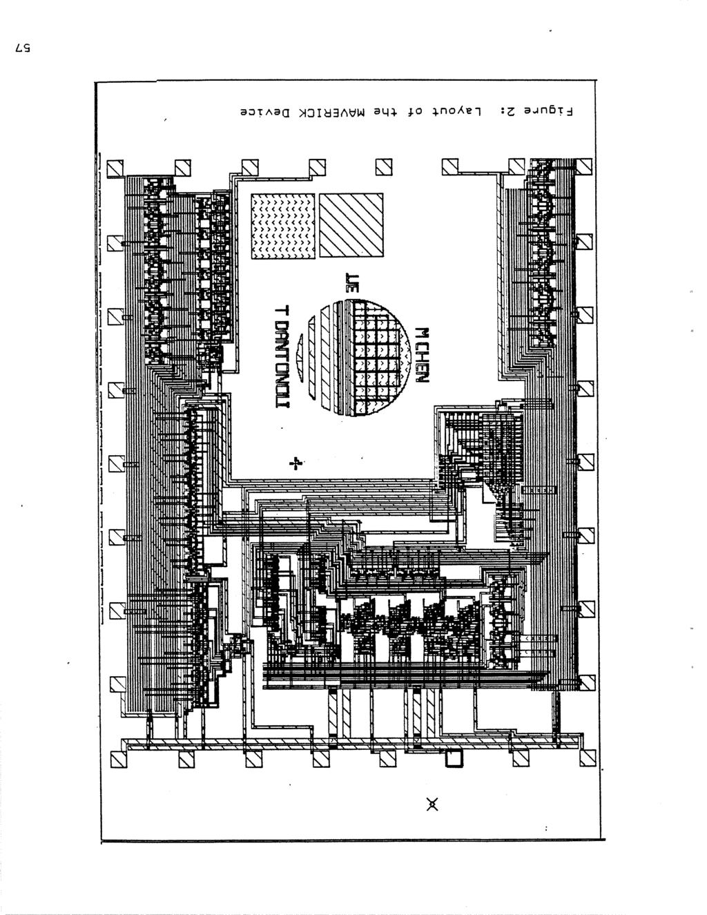
4 accumulator contains one of the binary numbers (say 1100). The second binary number is contained in the lower four bits of the MDR. The instruction for the NOR operation of the accumulator with 0110 is then The ACC will contain 0001 after after the instruction has been executed. The arithmatic unit is composed of an adder/subtractor module and logic modules. The adder/subtractor module consists of a standard 4-bit ripple, full adder. Some simple input logic was added to realize the increment, decrement and subtract functions. Logic modules consist of a series of NOR gates, inverters and NAND gates to perform bit by bit Boolean logic operations. All circuit schematics can be found in the Appendix in Figures Al - A7. LAYOUT/VERIF ICAT ION Device layout was performed on an Apollo workstation using ChipGraph graphics editor. MOSIS two lambda (lambda 2 microns) design rules were followed. This allowed the design rule checker on the workstation to be utilized. The layout was intended for fabrication with a self-aligned, poly-gate NMOS process using enhancement mode loads. A poly-gate PMOS process may also be used. Positive logic was implemented with 5v as logic high and Ov as logic low. The length to width ratio of all pull-up transistors was loum/4um while all pull-down transistors were 4um/Bum. All modules were full custom designs. The control unit was laid o~it as a programmable logic array (PLA) to facilitate quick changes as the design was modified. Figure 1 illustrates the block diagram of the MAVERICK device which indicates the general flow of data. A complete layout of the device as completed in February 1990 is shown in Figure 2. The Appendix contains more detailed layouts of the individual modules in Figures AS - A12 The device operation was verified by breadboarding with the 74 OO series CMOS components listed in Table 2. I Table 2 I I 74HC00 Quad 2 Input NAND Gate I I 74HC02 Quad 2 Input NOR Gate I 74HC04 Hex Inverter I I 74HC125 Quad Tn-State Buffer I I 74HC283 4-Bit Ripple Full-Adder I I 74HC373 Octal Transparent D Flip Flops I I 74HC86 Quad Exclusive OR Gate I 74HC Stage Ripple Counter I 74HC Decoder I 54
5 RESULTS Breadboard operation indicated that the original layout of the MAVERICK device would not operate correctly due to insufficient control of data with tristate buffers. This refers to the original use of tristate buffers to charge nodes to logic highs or lows. When the devices were disabled, floating nodes were created. Charge on these nodes leaked over short periods of time resulting in inconsistent device operation. Modifications to the breadboard design resolved this issue by placing registers at floating nodes to maintain logic levels. Several modifications to the original layout are therefore, necessary. This will consist of the addition of a temporary register and tristate buffer for addressable load operations. An obsolete tristate buffer will also need to be removed. The original layout also contained some logic circuitry to test the inputs and outputs of the MAR to check when they were equal. READ and WRITE lines were enabled when this condition was true. Redesign of the device eliminated the need for this circuitry. The PLA decoder will also need to be modified to reflect the necessary changes. The original photomask layout in Figure 2 indicates the points where changes need to be made. CONCLUSI ONS Breadboarding the MAVERICK device revealed several errors in the original photomask layout of the MAVERICK device. These errors were corrected on the breadboard to result in a fully, operational device. It is now necessary to revise the original layout to reflect the design changes. At that point, fabrication with an enhancement mode NMOS process will be possible. ACKNOWL EDGMENTS The author would like to thank the Microelectronic Engineering Department at the Rochester Institute of Technology for obtaining the necessary discrete CMOS parts. Thanks to Jim Kleffner of Motorola, INC in Austin, Texas for obtaining some hard to find 4-bit full adders. Special thanks to MIGUEL CHEN for his contributions to the design and layout of the MAVERICK device. REFERENCES [1] Kain, Richard Y.. Computer Architecture: Software and Hardware. New Jersey: Prentice Hall,
6 >i Figure 1: Slock Di~grem of 4 bit Microprocessor~ 56
7 U,
3. Implementing Logic in CMOS
 3. Implementing Logic in CMOS 3. Implementing Logic in CMOS Jacob Abraham Department of Electrical and Computer Engineering The University of Texas at Austin VLSI Design Fall 27 September, 27 ECE Department,
Dec Hex Bin ORG ; ZERO. Introduction To Computing
 Dec Hex Bin 0 0 00000000 ORG ; ZERO Introduction To Computing OBJECTIVES this chapter enables the student to: Convert any number from base 2, base 10, or base 16 to any of the other two bases. Add and
BUILDING BLOCKS OF A BASIC MICROPROCESSOR. Part 1 PowerPoint Format of Lecture 3 of Book
 BUILDING BLOCKS OF A BASIC MICROPROCESSOR Part PowerPoint Format of Lecture 3 of Book Decoder Tri-state device Full adder, full subtractor Arithmetic Logic Unit (ALU) Memories Example showing how to write
Reference Sheet for C112 Hardware
 Reference Sheet for C112 Hardware 1 Boolean Algebra, Gates and Circuits Autumn 2016 Basic Operators Precedence : (strongest),, + (weakest). AND A B R 0 0 0 0 1 0 1 0 0 1 1 1 OR + A B R 0 0 0 0 1 1 1 0
Microcomputers. Outline. Number Systems and Digital Logic Review
 Microcomputers Number Systems and Digital Logic Review Lecture 1-1 Outline Number systems and formats Common number systems Base Conversion Integer representation Signed integer representation Binary coded
COMPUTER ARCHITECTURE AND ORGANIZATION Register Transfer and Micro-operations 1. Introduction A digital system is an interconnection of digital
 Register Transfer and Micro-operations 1. Introduction A digital system is an interconnection of digital hardware modules that accomplish a specific information-processing task. Digital systems vary in
CPU ARCHITECTURE. QUESTION 1 Explain how the width of the data bus and system clock speed affect the performance of a computer system.
 CPU ARCHITECTURE QUESTION 1 Explain how the width of the data bus and system clock speed affect the performance of a computer system. ANSWER 1 Data Bus Width the width of the data bus determines the number
CS 31: Intro to Systems Digital Logic. Kevin Webb Swarthmore College February 3, 2015
 CS 31: Intro to Systems Digital Logic Kevin Webb Swarthmore College February 3, 2015 Reading Quiz Today Hardware basics Machine memory models Digital signals Logic gates Circuits: Borrow some paper if
CS 31: Intro to Systems Digital Logic. Kevin Webb Swarthmore College February 2, 2016
 CS 31: Intro to Systems Digital Logic Kevin Webb Swarthmore College February 2, 2016 Reading Quiz Today Hardware basics Machine memory models Digital signals Logic gates Circuits: Borrow some paper if
Microcontroller Systems
 µcontroller systems 1 / 43 Microcontroller Systems Engineering Science 2nd year A2 Lectures Prof David Murray david.murray@eng.ox.ac.uk www.robots.ox.ac.uk/ dwm/courses/2co Michaelmas 2014 µcontroller
UPY14602-DIGITAL ELECTRONICS AND MICROPROCESSORS Lesson Plan
 UPY14602-DIGITAL ELECTRONICS AND MICROPROCESSORS Lesson Plan UNIT I - NUMBER SYSTEMS AND LOGIC GATES Introduction to decimal- Binary- Octal- Hexadecimal number systems-inter conversions-bcd code- Excess
Prototype of SRAM by Sergey Kononov, et al.
 Prototype of SRAM by Sergey Kononov, et al. 1. Project Overview The goal of the project is to create a SRAM memory layout that provides maximum utilization of the space on the 1.5 by 1.5 mm chip. Significant
session 7. Datapath Design
 General Objective: Determine the hardware requirement of a digital computer based on its instruction set. Specific Objectives: Describe the general concepts in designing the data path of a digital computer
1 MALP ( ) Unit-1. (1) Draw and explain the internal architecture of 8085.
 Unit-1. (1) Draw and explain the internal architecture of 8085.") (1) Draw and explain the internal architecture of 8085. The architecture of 8085 Microprocessor is shown in figure given below. The internal architecture of 8085 includes following section ALU-Arithmetic
(1) Draw and explain the internal architecture of 8085. The architecture of 8085 Microprocessor is shown in figure given below. The internal architecture of 8085 includes following section ALU-Arithmetic
1. INTRODUCTION TO MICROPROCESSOR AND MICROCOMPUTER ARCHITECTURE:
 1. INTRODUCTION TO MICROPROCESSOR AND MICROCOMPUTER ARCHITECTURE: A microprocessor is a programmable electronics chip that has computing and decision making capabilities similar to central processing unit
Segment 1A. Introduction to Microcomputer and Microprocessor
 Segment 1A Introduction to Microcomputer and Microprocessor 1.1 General Architecture of a Microcomputer System: The term microcomputer is generally synonymous with personal computer, or a computer that
DIRECTORATE OF TECHNICAL EDUCATION DIPLOMA IN ELECTRICAL AND ELECTRONICS ENGINEERING II YEAR M SCHEME IV SEMESTER.
 DIRECTORATE OF TECHNICAL EDUCATION DIPLOMA IN ELECTRICAL AND ELECTRONICS ENGINEERING II YEAR M SCHEME IV SEMESTER 2015 2016 onwards DIGITAL ELECTRONICS CURRICULUM DEVELOPMENT CENTRE Curriculum Development
Injntu.com Injntu.com Injntu.com R16
 1. a) What are the three methods of obtaining the 2 s complement of a given binary (3M) number? b) What do you mean by K-map? Name it advantages and disadvantages. (3M) c) Distinguish between a half-adder
COSC 243. Computer Architecture 1. COSC 243 (Computer Architecture) Lecture 6 - Computer Architecture 1 1
 Lecture 6 - Computer Architecture 1 1") COSC 243 Computer Architecture 1 COSC 243 (Computer Architecture) Lecture 6 - Computer Architecture 1 1 Overview Last Lecture Flip flops This Lecture Computers Next Lecture Instruction sets and addressing
COSC 243 Computer Architecture 1 COSC 243 (Computer Architecture) Lecture 6 - Computer Architecture 1 1 Overview Last Lecture Flip flops This Lecture Computers Next Lecture Instruction sets and addressing
Roberto Muscedere Images and Text Portions 2003 Prentice Hall 1
 Microcomputer Structure and Operation Chapter 5 A Microprocessor ( P) contains the controller, ALU and internal registers A Microcomputer ( C) contains a microprocessor, memory (RAM, ROM, etc), input and
6. Latches and Memories
 6 Latches and Memories This chapter . RS Latch The RS Latch, also called Set-Reset Flip Flop (SR FF), transforms a pulse into a continuous state. The RS latch can be made up of two interconnected
UNIT-III REGISTER TRANSFER LANGUAGE AND DESIGN OF CONTROL UNIT
 UNIT-III 1 KNREDDY UNIT-III REGISTER TRANSFER LANGUAGE AND DESIGN OF CONTROL UNIT Register Transfer: Register Transfer Language Register Transfer Bus and Memory Transfers Arithmetic Micro operations Logic
ECE 2030B 1:00pm Computer Engineering Spring problems, 5 pages Exam Two 10 March 2010
 Instructions: This is a closed book, closed note exam. Calculators are not permitted. If you have a question, raise your hand and I will come to you. Please work the exam in pencil and do not separate
File: 'ReportV37P-CT89533DanSuo.doc' CMPEN 411, Spring 2013, Homework Project 9 chip, 'Tiny Chip' fabricated through MOSIS program
 MOSIS Chip Test Report Dan Suo File: 'ReportV37P-CT89533DanSuo.doc' CMPEN 411, Spring 2013, Homework Project 9 chip, 'Tiny Chip' fabricated through MOSIS program Technology: 0.5um CMOS, ON Semiconductor
DIGITAL ELECTRONICS. Vayu Education of India
 DIGITAL ELECTRONICS ARUN RANA Assistant Professor Department of Electronics & Communication Engineering Doon Valley Institute of Engineering & Technology Karnal, Haryana (An ISO 9001:2008 ) Vayu Education
UNIT - V MEMORY P.VIDYA SAGAR ( ASSOCIATE PROFESSOR) Department of Electronics and Communication Engineering, VBIT
 Department of Electronics and Communication Engineering, VBIT") UNIT - V MEMORY P.VIDYA SAGAR ( ASSOCIATE PROFESSOR) contents Memory: Introduction, Random-Access memory, Memory decoding, ROM, Programmable Logic Array, Programmable Array Logic, Sequential programmable
UNIT - V MEMORY P.VIDYA SAGAR ( ASSOCIATE PROFESSOR) contents Memory: Introduction, Random-Access memory, Memory decoding, ROM, Programmable Logic Array, Programmable Array Logic, Sequential programmable
END-TERM EXAMINATION
 (Please Write your Exam Roll No. immediately) END-TERM EXAMINATION DECEMBER 2006 Exam. Roll No... Exam Series code: 100919DEC06200963 Paper Code: MCA-103 Subject: Digital Electronics Time: 3 Hours Maximum
Basic Processing Unit: Some Fundamental Concepts, Execution of a. Complete Instruction, Multiple Bus Organization, Hard-wired Control,
 UNIT - 7 Basic Processing Unit: Some Fundamental Concepts, Execution of a Complete Instruction, Multiple Bus Organization, Hard-wired Control, Microprogrammed Control Page 178 UNIT - 7 BASIC PROCESSING
Module 5 - CPU Design
 Module 5 - CPU Design Lecture 1 - Introduction to CPU The operation or task that must perform by CPU is: Fetch Instruction: The CPU reads an instruction from memory. Interpret Instruction: The instruction
Introduction to general architectures of 8 and 16 bit micro-processor and micro-controllers
 Introduction to general architectures of 8 and 16 bit micro-processor and micro-controllers A microcontroller is a microprocessor with inbuilt peripherals.a microcontroller can also be compared with a
ECE 2030D Computer Engineering Spring problems, 5 pages Exam Two 8 March 2012
 Instructions: This is a closed book, closed note exam. Calculators are not permitted. If you have a question, raise your hand and I will come to you. Please work the exam in pencil and do not separate
Computer Architecture: Part III. First Semester 2013 Department of Computer Science Faculty of Science Chiang Mai University
 Computer Architecture: Part III First Semester 2013 Department of Computer Science Faculty of Science Chiang Mai University Outline Decoders Multiplexers Registers Shift Registers Binary Counters Memory
CHAPTER 5 : Introduction to Intel 8085 Microprocessor Hardware BENG 2223 MICROPROCESSOR TECHNOLOGY
 CHAPTER 5 : Introduction to Intel 8085 Hardware BENG 2223 MICROPROCESSOR TECHNOLOGY The 8085A(commonly known as the 8085) : Was first introduced in March 1976 is an 8-bit microprocessor with 16-bit address
Digital IP Cell 8-bit Microcontroller PE80
 1. Description The is a Z80 compliant processor soft-macro - IP block that can be implemented in digital or mixed signal ASIC designs. The Z80 and its derivatives and clones make up one of the most commonly
Computer Systems Organization
 The IAS (von Neumann) Machine Computer Systems Organization Input Output Equipment Stored Program concept Main memory storing programs and data ALU operating on binary data Control unit interpreting instructions
CS/ECE 252: INTRODUCTION TO COMPUTER ENGINEERING UNIVERSITY OF WISCONSIN MADISON
 CS/ECE 252: INTRODUCTION TO COMPUTER ENGINEERING UNIVERSITY OF WISCONSIN MADISON Prof. Gurindar Sohi TAs: Junaid Khalid and Pradip Vallathol Midterm Examination 2 In Class (50 minutes) Friday, October
Dynamic CMOS Logic Gate
 Dynamic CMOS Logic Gate In dynamic CMOS logic a single clock can be used to accomplish both the precharge and evaluation operations When is low, PMOS pre-charge transistor Mp charges Vout to Vdd, since
Register Transfer and Micro-operations
 Register Transfer Language Register Transfer Bus Memory Transfer Micro-operations Some Application of Logic Micro Operations Register Transfer and Micro-operations Learning Objectives After reading this
Concept of Memory. The memory of computer is broadly categories into two categories:
 Concept of Memory We have already mentioned that digital computer works on stored programmed concept introduced by Von Neumann. We use memory to store the information, which includes both program and data.
Lab 16: Data Busses, Tri-State Outputs and Memory
 Lab 16: Data Busses, Tri-State Outputs and Memory UC Davis Physics 116B Rev. 0.9, Feb. 2006 1 Introduction 1.1 Data busses Data busses are ubiquitous in systems which must communicate digital data. Examples
REGISTER TRANSFER LANGUAGE
 REGISTER TRANSFER LANGUAGE The operations executed on the data stored in the registers are called micro operations. Classifications of micro operations Register transfer micro operations Arithmetic micro
Unit II Basic Computer Organization
 1. Define the term. Internal Organization-The internal organization of a digital system is defined by the sequence of microoperations it performs on data stored in its registers. Program- A program is
A3 Computer Architecture
 A3 Computer Architecture Engineering Science 3rd year A3 Lectures Prof David Murray david.murray@eng.ox.ac.uk www.robots.ox.ac.uk/ dwm/courses/3co Michaelmas 2000 1 / 1 2: Introduction to the CPU 3A3 Michaelmas
How a Digital Binary Adder Operates
 Overview of a Binary Adder How a Digital Binary Adder Operates By: Shawn R Moser A binary adder is a digital electronic component that is used to perform the addition of two binary numbers and return the
2. (a) Compare the characteristics of a floppy disk and a hard disk. (b) Discuss in detail memory interleaving. [8+7]
![2. (a) Compare the characteristics of a floppy disk and a hard disk. (b) Discuss in detail memory interleaving. [8+7]](/thumbs/96/127320205.jpg "2. (a) Compare the characteristics of a floppy disk and a hard disk. (b) Discuss in detail memory interleaving. [8+7]") Code No: A109211202 R09 Set No. 2 1. (a) Explain the purpose of the following registers: i. IR ii. PC iii. MDR iv. MAR. (b) Explain with an example the steps in subtraction of two n-digit unsigned numbers.
Code No: A109211202 R09 Set No. 2 1. (a) Explain the purpose of the following registers: i. IR ii. PC iii. MDR iv. MAR. (b) Explain with an example the steps in subtraction of two n-digit unsigned numbers.
csitnepal Unit 3 Basic Computer Organization and Design
 Unit 3 Basic Computer Organization and Design Introduction We introduce here a basic computer whose operation can be specified by the resister transfer statements. Internal organization of the computer
Compact Integrated Processor
 Compact Integrated Processor EE498 Report Senior Design II Jared Hayes Nick Repetti Jason Silic Faculty Advisor: Dr. R. Jacob Baker 12 May 2015 1 Table of Contents 1. Introduction......3 1.1. Introduction......3
CHAPTER SIX BASIC COMPUTER ORGANIZATION AND DESIGN
 CHAPTER SIX BASIC COMPUTER ORGANIZATION AND DESIGN 6.1. Instruction Codes The organization of a digital computer defined by: 1. The set of registers it contains and their function. 2. The set of instructions
REGISTER TRANSFER AND MICROOPERATIONS
 REGISTER TRANSFER AND MICROOPERATIONS Register Transfer Language Register Transfer Bus and Memory Transfers Arithmetic Microoperations Logic Microoperations Shift Microoperations Arithmetic Logic Shift
Introduction to Computer Science. Homework 1
 Introduction to Computer Science Homework. In each circuit below, the rectangles represent the same type of gate. Based on the input and output information given, identify whether the gate involved is
COMPUTER ORGANIZATION
 COMPUTER ORGANIZATION INDEX UNIT-II PPT SLIDES Srl. No. Module as per Session planner Lecture No. PPT Slide No. 1. Register Transfer language 2. Register Transfer Bus and memory transfers 3. Arithmetic
Introduction to CPU Design
 ١ Introduction to CPU Design Computer Organization & Assembly Language Programming Dr Adnan Gutub aagutub at uqu.edu.sa [Adapted from slides of Dr. Kip Irvine: Assembly Language for Intel-Based Computers]
B.Tech II Year I Semester (R13) Regular Examinations December 2014 DIGITAL LOGIC DESIGN
 Regular Examinations December 2014 DIGITAL LOGIC DESIGN") B.Tech II Year I Semester () Regular Examinations December 2014 (Common to IT and CSE) (a) If 1010 2 + 10 2 = X 10, then X is ----- Write the first 9 decimal digits in base 3. (c) What is meant by don
B.Tech II Year I Semester () Regular Examinations December 2014 (Common to IT and CSE) (a) If 1010 2 + 10 2 = X 10, then X is ----- Write the first 9 decimal digits in base 3. (c) What is meant by don
Midterm Project Design of 4 Bit ALU Fall 2001
 Midterm Project Design of 4 Bit ALU Fall 2001 By K.Narayanan George Washington University E.C.E Department K.Narayanan Fall 2001 1 Midterm Project... 1 Design of 4 Bit ALU... 1 Abstract... 3 1.2 Specification:...
R10. II B. Tech I Semester, Supplementary Examinations, May
 SET - 1 1. a) Convert the following decimal numbers into an equivalent binary numbers. i) 53.625 ii) 4097.188 iii) 167 iv) 0.4475 b) Add the following numbers using 2 s complement method. i) -48 and +31
Spiral 2-8. Cell Layout
 2-8.1 Spiral 2-8 Cell Layout 2-8.2 Learning Outcomes I understand how a digital circuit is composed of layers of materials forming transistors and wires I understand how each layer is expressed as geometric
2. List the five interrupt pins available in INTR, TRAP, RST 7.5, RST 6.5, RST 5.5.
 DHANALAKSHMI COLLEGE OF ENGINEERING DEPARTMENT OF ELECTRICAL AND ELECTRONICS ENGINEERING EE6502- MICROPROCESSORS AND MICROCONTROLLERS UNIT I: 8085 PROCESSOR PART A 1. What is the need for ALE signal in
The Itanium Bit Microprocessor Report
 The Itanium - 1986 8 Bit Microprocessor Report By PRIYANK JAIN (02010123) Group # 11 Under guidance of Dr. J. K. Deka & Dr. S. B. Nair Department of Computer Science & Engineering Indian Institute of Technology,
The 9S12 in Expanded Mode - Using MSI logic to build ports Huang Chapter 14
 The 9S12 in Expanded Mode - Using MSI logic to build ports Huang Chapter 14 Using MSI Logic To Build An Output Port Many designs use standard MSI logic for microprocessor expansion This provides an inexpensive
Blog -
 . Instruction Codes Every different processor type has its own design (different registers, buses, microoperations, machine instructions, etc) Modern processor is a very complex device It contains Many
CAD4 The ALU Fall 2009 Assignment. Description
 CAD4 The ALU Fall 2009 Assignment To design a 16-bit ALU which will be used in the datapath of the microprocessor. This ALU must support two s complement arithmetic and the instructions in the baseline
CS101 Lecture 25: The Machinery of Computation: Computer Architecture. John Magee 29 July 2013 Some material copyright Jones and Bartlett
 CS101 Lecture 25: The Machinery of Computation: Computer Architecture John Magee 29 July 2013 Some material copyright Jones and Bartlett 1 Overview/Questions What did we do last time? Can we relate this
EE 3170 Microcontroller Applications
 EE 3170 Microcontroller Applications Lecture 4 : Processors, Computers, and Controllers - 1.2 (reading assignment), 1.3-1.5 Based on slides for ECE3170 by Profs. Kieckhafer, Davis, Tan, and Cischke Outline
Combinational and sequential circuits (learned in Chapters 1 and 2) can be used to create simple digital systems.
 can be used to create simple digital systems.") REGISTER TRANSFER AND MICROOPERATIONS Register Transfer Language Register Transfer Bus and Memory Transfers Arithmetic Microoperations Logic Microoperations Shift Microoperations Arithmetic Logic Shift
REGISTER TRANSFER AND MICROOPERATIONS Register Transfer Language Register Transfer Bus and Memory Transfers Arithmetic Microoperations Logic Microoperations Shift Microoperations Arithmetic Logic Shift
Chapter 2 Logic Gates and Introduction to Computer Architecture
 Chapter 2 Logic Gates and Introduction to Computer Architecture 2.1 Introduction The basic components of an Integrated Circuit (IC) is logic gates which made of transistors, in digital system there are
ASSEMBLY LANGUAGE MACHINE ORGANIZATION
 ASSEMBLY LANGUAGE MACHINE ORGANIZATION CHAPTER 3 1 Sub-topics The topic will cover: Microprocessor architecture CPU processing methods Pipelining Superscalar RISC Multiprocessing Instruction Cycle Instruction
CS429: Computer Organization and Architecture
 CS429: Computer Organization and Architecture Dr. Bill Young Department of Computer Sciences University of Texas at Austin Last updated: January 2, 2018 at 11:23 CS429 Slideset 5: 1 Topics of this Slideset
Control Unit: The control unit provides the necessary timing and control Microprocessor resembles a CPU exactly.
 Unit I 8085 and 8086 PROCESSOR Introduction to microprocessor A microprocessor is a clock-driven semiconductor device consisting of electronic logic circuits manufactured by using either a large-scale
CHAPTER 4: Register Transfer Language and Microoperations
 CS 224: Computer Organization S.KHABET CHAPTER 4: Register Transfer Language and Microoperations Outline Register Transfer Language Register Transfer Bus and Memory Transfers Arithmetic Microoperations
CHAPTER 12 ARRAY SUBSYSTEMS [ ] MANJARI S. KULKARNI
![CHAPTER 12 ARRAY SUBSYSTEMS [ ] MANJARI S. KULKARNI](/thumbs/76/73997056.jpg "CHAPTER 12 ARRAY SUBSYSTEMS [ ] MANJARI S. KULKARNI") CHAPTER 2 ARRAY SUBSYSTEMS [2.4-2.9] MANJARI S. KULKARNI OVERVIEW Array classification Non volatile memory Design and Layout Read-Only Memory (ROM) Pseudo nmos and NAND ROMs Programmable ROMS PROMS, EPROMs,
CHAPTER 2 ARRAY SUBSYSTEMS [2.4-2.9] MANJARI S. KULKARNI OVERVIEW Array classification Non volatile memory Design and Layout Read-Only Memory (ROM) Pseudo nmos and NAND ROMs Programmable ROMS PROMS, EPROMs,
Computer Systems. Binary Representation. Binary Representation. Logical Computation: Boolean Algebra
 Binary Representation Computer Systems Information is represented as a sequence of binary digits: Bits What the actual bits represent depends on the context: Seminar 3 Numerical value (integer, floating
CMOS Process Flow. Layout CAD Tools
 CMOS Process Flow See supplementary power point file for animated CMOS process flow (see class ece410 website and/or* http://www.multimedia.vt.edu/ee5545/): This file should be viewed as a slide show It
3. The high voltage level of a digital signal in positive logic is : a) 1 b) 0 c) either 1 or 0
 1 b) 0 c) either 1 or 0") 1. The number of level in a digital signal is: a) one b) two c) four d) ten 2. A pure sine wave is : a) a digital signal b) analog signal c) can be digital or analog signal d) neither digital nor analog
1. The number of level in a digital signal is: a) one b) two c) four d) ten 2. A pure sine wave is : a) a digital signal b) analog signal c) can be digital or analog signal d) neither digital nor analog
Microprocessors/Microcontrollers
 Microprocessors/Microcontrollers A central processing unit (CPU) fabricated on one or more chips, containing the basic arithmetic, logic, and control elements of a computer that are required for processing
SIR C.R.REDDY COLLEGE OF ENGINEERING, ELURU DEPARTMENT OF INFORMATION TECHNOLOGY LESSON PLAN
 SIR C.R.REDDY COLLEGE OF ENGINEERING, ELURU DEPARTMENT OF INFORMATION TECHNOLOGY LESSON PLAN SUBJECT: CSE 2.1.6 DIGITAL LOGIC DESIGN CLASS: 2/4 B.Tech., I SEMESTER, A.Y.2017-18 INSTRUCTOR: Sri A.M.K.KANNA
Computer Organization and Levels of Abstraction
 Computer Organization and Levels of Abstraction Announcements Today: PS 7 Lab 8: Sound Lab tonight bring machines and headphones! PA 7 Tomorrow: Lab 9 Friday: PS8 Today (Short) Floating point review Boolean
1. Prove that if you have tri-state buffers and inverters, you can build any combinational logic circuit. [4]
![1. Prove that if you have tri-state buffers and inverters, you can build any combinational logic circuit. [4]](/thumbs/81/83055464.jpg "1. Prove that if you have tri-state buffers and inverters, you can build any combinational logic circuit. [4]") HW 3 Answer Key 1. Prove that if you have tri-state buffers and inverters, you can build any combinational logic circuit. [4] You can build a NAND gate from tri-state buffers and inverters and thus you
HW 3 Answer Key 1. Prove that if you have tri-state buffers and inverters, you can build any combinational logic circuit. [4] You can build a NAND gate from tri-state buffers and inverters and thus you
ECE 331: N0. Professor Andrew Mason Michigan State University. Opening Remarks
 ECE 331: N0 ECE230 Review Professor Andrew Mason Michigan State University Spring 2013 1.1 Announcements Opening Remarks HW1 due next Mon Labs begin in week 4 No class next-next Mon MLK Day ECE230 Review
2 MARKS Q&A 1 KNREDDY UNIT-I
 2 MARKS Q&A 1 KNREDDY UNIT-I 1. What is bus; list the different types of buses with its function. A group of lines that serves as a connecting path for several devices is called a bus; TYPES: ADDRESS BUS,
CS 101, Mock Computer Architecture
 CS 101, Mock Computer Architecture Computer organization and architecture refers to the actual hardware used to construct the computer, and the way that the hardware operates both physically and logically
Software and Hardware
 Software and Hardware Numbers At the most fundamental level, a computer manipulates electricity according to specific rules To make those rules produce something useful, we need to associate the electrical
Scheme G. Sample Test Paper-I
 Sample Test Paper-I Marks : 25 Times:1 Hour 1. All questions are compulsory. 2. Illustrate your answers with neat sketches wherever necessary. 3. Figures to the right indicate full marks. 4. Assume suitable
SCRAM Introduction. Philipp Koehn. 19 February 2018
 SCRAM Introduction Philipp Koehn 19 February 2018 This eek 1 Fully work through a computer circuit assembly code Simple but Complete Random Access Machine (SCRAM) every instruction is 8 bit 4 bit for op-code:
1. Draw general diagram of computer showing different logical components (3)
") Tutorial 1 1. Draw general diagram of computer showing different logical components (3) 2. List at least three input devices (1.5) 3. List any three output devices (1.5) 4. Fill the blank cells of the
Tutorial 1 1. Draw general diagram of computer showing different logical components (3) 2. List at least three input devices (1.5) 3. List any three output devices (1.5) 4. Fill the blank cells of the
REGISTER TRANSFER AND MICROOPERATIONS
 1 REGISTER TRANSFER AND MICROOPERATIONS Register Transfer Language Register Transfer Bus and Memory Transfers Arithmetic Microoperations Logic Microoperations Shift Microoperations Arithmetic Logic Shift
Microcomputer Architecture and Programming
 IUST-EE (Chapter 1) Microcomputer Architecture and Programming 1 Outline Basic Blocks of Microcomputer Typical Microcomputer Architecture The Single-Chip Microprocessor Microprocessor vs. Microcontroller
EXPERIMENT NUMBER 11 REGISTERED ALU DESIGN
 11-1 EXPERIMENT NUMBER 11 REGISTERED ALU DESIGN Purpose Extend the design of the basic four bit adder to include other arithmetic and logic functions. References Wakerly: Section 5.1 Materials Required
PSIM: Processor SIMulator (version 4.2)
") PSIM: Processor SIMulator (version 4.2) by Charles E. Stroud, Professor Dept. of Electrical & Computer Engineering Auburn University July 23, 2003 ABSTRACT A simulator for a basic stored program computer
PSIM: Processor SIMulator (version 4.2) by Charles E. Stroud, Professor Dept. of Electrical & Computer Engineering Auburn University July 23, 2003 ABSTRACT A simulator for a basic stored program computer
ESE370: Circuit-Level Modeling, Design, and Optimization for Digital Systems
 ESE370: Circuit-Level Modeling, Design, and Optimization for Digital Systems Lec 26: November 9, 2018 Memory Overview Dynamic OR4! Precharge time?! Driving input " With R 0 /2 inverter! Driving inverter
 An Overview of Microprocessor The first question comes in a mind "What is a microprocessor?. Let us start with a more familiar term computer. A digital computer is an electronic machine capable of quickly
One and a half hours. Section A is COMPULSORY UNIVERSITY OF MANCHESTER SCHOOL OF COMPUTER SCIENCE
 COMP 12111 One and a half hours Section A is COMPULSORY UNIVERSITY OF MANCHESTER SCHOOL OF COMPUTER SCIENCE Fundamentals of Computer Engineering Date: Monday 23rd January 2017 Time: 09:45-11:15 Answer
CS 2461: Computer Architecture I
 Computer Architecture is... CS 2461: Computer Architecture I Instructor: Prof. Bhagi Narahari Dept. of Computer Science Course URL: www.seas.gwu.edu/~bhagiweb/cs2461/ Instruction Set Architecture Organization
Systems Programming. Lecture 2 Review of Computer Architecture I
 Systems Programming www.atomicrhubarb.com/systems Lecture 2 Review of Computer Architecture I In The Book Patt & Patel Chapter 1,2,3 (review) Outline Binary Bit Numbering Logical operations 2's complement
2015 Paper E2.1: Digital Electronics II
 s 2015 Paper E2.1: Digital Electronics II Answer ALL questions. There are THREE questions on the paper. Question ONE counts for 40% of the marks, other questions 30% Time allowed: 2 hours (Not to be removed
Von Neumann Architecture
 Von Neumann Architecture Assist lecturer Donya A. Khalid Lecture 2 2/29/27 Computer Organization Introduction In 945, just after the World War, Jon Von Neumann proposed to build a more flexible computer.
CONTENTS CHAPTER 1: NUMBER SYSTEM. Foreword...(vii) Preface... (ix) Acknowledgement... (xi) About the Author...(xxiii)
 Preface... (ix) Acknowledgement... (xi) About the Author...(xxiii)") CONTENTS Foreword...(vii) Preface... (ix) Acknowledgement... (xi) About the Author...(xxiii) CHAPTER 1: NUMBER SYSTEM 1.1 Digital Electronics... 1 1.1.1 Introduction... 1 1.1.2 Advantages of Digital Systems...
CONTENTS Foreword...(vii) Preface... (ix) Acknowledgement... (xi) About the Author...(xxiii) CHAPTER 1: NUMBER SYSTEM 1.1 Digital Electronics... 1 1.1.1 Introduction... 1 1.1.2 Advantages of Digital Systems...
St.MARTIN S ENGINEERING COLLEGE Dhulapally, Secunderabad
 St.MARTIN S ENGINEERING COLLEGE Dhulapally, Secunderabad-500 014 Subject: Digital Design Using Verilog Hdl Class : ECE-II Group A (Short Answer Questions) UNIT-I 1 Define verilog HDL? 2 List levels of
Code No: R Set No. 1
 Code No: R059210504 Set No. 1 II B.Tech I Semester Supplementary Examinations, February 2007 DIGITAL LOGIC DESIGN ( Common to Computer Science & Engineering, Information Technology and Computer Science
The Memory Component
 The Computer Memory Chapter 6 forms the first of a two chapter sequence on computer memory. Topics for this chapter include. 1. A functional description of primary computer memory, sometimes called by
R a) Simplify the logic functions from binary to seven segment display code converter (8M) b) Simplify the following using Tabular method
 Simplify the logic functions from binary to seven segment display code converter (8M) b) Simplify the following using Tabular method") SET - 1 1. a) Convert the decimal number 250.5 to base 3, base 4 b) Write and prove de-morgan laws c) Implement two input EX-OR gate from 2 to 1 multiplexer (3M) d) Write the demerits of PROM (3M) e) What
SET - 1 1. a) Convert the decimal number 250.5 to base 3, base 4 b) Write and prove de-morgan laws c) Implement two input EX-OR gate from 2 to 1 multiplexer (3M) d) Write the demerits of PROM (3M) e) What