Beyond Chip Stacking---Quilt Packaging Enabled 3D Systems
|
|
|
- Darlene Woods
- 5 years ago
- Views:
Transcription

1 Beyond Chip Stacking---Quilt Packaging Enabled 3D Systems Jason Kulick, President & Co-Founder (South Bend, IN) May 3, New England IMAPS Symposium
2 Presentation Overview 1. Introduction to Indiana Integrated Circuits 2. Introduction to Quilt Packaging interconnect technology & fabrication description 3. Brief overview of QP electrical & mechanical performance & reliability 4. 3D Systems enabled using Quilt Packaging 5. Summary/Discussion 2
3 Indiana Integrated Circuits, LLC (IIC) Formed to commercialize Quilt Packaging (QP) a ground breaking packaging technology invented at Notre Dame. Founded by Kulick & Bernstein (2009) Main office South Bend, IN at Innovation Park (also CO & NC) IIC has experienced steady growth with customers & partners across multiple industry sectors since early in it s inception. Operations funded directly through revenue growth and through equity investment (Series A closed late 2015). The QP process is commercially available at RTI International. Process development for medium volume requirements is ongoing at Rogue Valley Microdevices in Medford, OR. 3
 IIC works with customers to integrate")


4 IIC Business Model--Licensing (supported by prototyping) IIC works with customers to integrate QP into their systems. First-adopters have been aerospace/defense applications. QP is platform technology (3D, microwave, power, optical, biomed, more) Expansion beyond DOD to commercial underway and more proprietary. 4
5 Existing Supply Chain Wafer Processing RTI International, Inc. ITAR compliant BEOL facility located in Durham/RTP, NC Wafer post-processing for deep etch, plating, CMP, singulation Si & SiC substrates from pieces up o 8 wafers IIC partner since 2012 Offering QP MPW service Can support up to 100 wafer starts per month Rogue Valley Microdevices, Inc. Pure-play MEMS foundry located in Medford, OR Wafer post-processing for thin film, etching, litho (deep etch coming) Multiple substrates, up to 8 wafers IIC partner since January 2015 (MIG Tech. Pitch win award) Can support several hundred wafer starts per month 5
6 Existing Supply Chain Assembly Automated Tooling: MRSI Systems, Inc. Global supplier of fullyautomated solutions for assembly of microelectronic devices High precision die attach & dispensing systems Demonstrated automated Quilt Package assembly on MRSI 705 system Working with since 2012 Based in Billerica, MA North American-based Low to Medium Volume Assembler Public announcement coming soon (Spring 2016) Leader in electronics design, manufacturing and aftermarket services Can support DOD applications 6


7 Existing Microchip Packaging Chip A Electrical Signal chpackage ip packa ge PC board A B Chip B Package Overall performance, cost, size and functionality of a system will be limited by.the off-chip interconnects. -International Technology Roadmap For Semiconductors Existing technologies waste: Power Time Money Space 7 Packaging has become a system constraint.


8 Quilt Packaging Interconnect Technology Package Electrical Signal Chip A Chip A Solder Chip B Quilt Packaging interconnect Chip B Quilt Packaging is a patented, direct edgeto-edge chip interconnect technology that can be implemented in disparate materials and technologies (Si, GaAs, InP, GaN/SiC, SiGe, GaSb,etc.) Quilt Packaging enables 10x to 100X improvement. Power--- 10x lower parasitic losses Time---10x faster Money---Order of magnitude total system cost savings Space---Dramatic form factor reduction Quilt Packaging enables new system designs 8

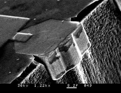
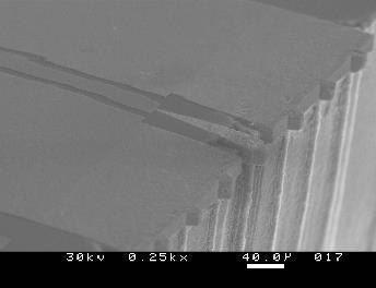
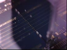
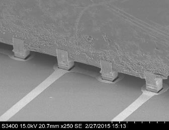
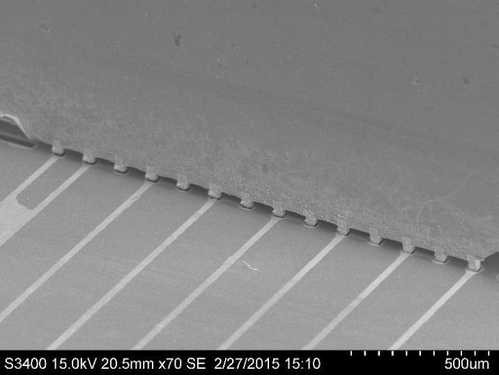
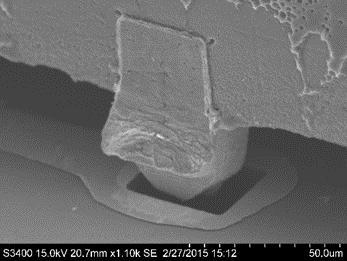
9 QP-Interconnect Structures Edge connection structures called nodules Solid metal, typically Cu, um wide, um thick 10 um pitch possible Customizable shapesincluding interlockingenables sub-micron chip alignment 9
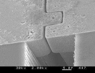

10 QP Customizable I/O 10


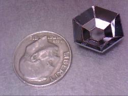
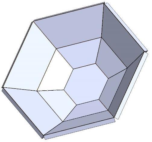
11 QP Supports Customized Geometries example - HexQP 11
 Nodule metallization; 5) Metal 1 deposition; 6) Singulation etch; 7) separation grinding; 8) Die connection; 9) Final quilt")
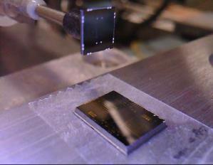
12 Quilt Packaging Process Overview QP Fabrication Process (starting at top left and following arrows to bottom: 1)Front end finished; 2) Nodules etched; 3) Dielectric insulating layer; 4) Nodule metallization; 5) Metal 1 deposition; 6) Singulation etch; 7) separation grinding; 8) Die connection; 9) Final quilt assembly.
 interconnects demonstrated Excellent RF/millimeter-wave, high speed digital performance: Less than 0.1 db S 21 from DC-100 GHz S 21 0.")
13 Quilt Packaging Electrical Performance (Performs as if it were an on-chip interconnect) Homogeneous (e.g. Si-Si, GaAs-GaAs) and heterogeneous (Si-GaAs, Si-InP, etc.) interconnects demonstrated Excellent RF/millimeter-wave, high speed digital performance: Less than 0.1 db S 21 from DC-100 GHz S db to 220 GHz 43 Gb/s eyes with no impairment Ultra-low parasitics Dense I/O pitch at chip edge (10 um pitch) Extremely high current-handling capacity > 10 A through 30 µm x 20 µm nodules without damage Si-GaAs CPW
 Thermal test -40 C to 125 C, 1000+ cycles, no failures Tested to 77K from ambient, no failures for mounted or un-mounted Pull testing requires large force before failure Four die connected;")
14 Quilt Packaging: Mechanical Performance Extremely robust mechanically Interconnected quilt can often be handled like larger chip (e.g. pick & place, etc.) Thermal test -40 C to 125 C, cycles, no failures Tested to 77K from ambient, no failures for mounted or un-mounted Pull testing requires large force before failure Four die connected; mechanical handling as if single chip Pull test: 50 µm x 20 µm nodules, 40 nodules per edge


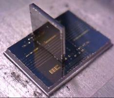
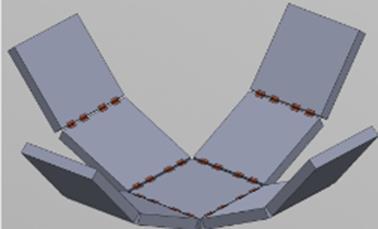
15 3DQP Variations: Orthogonal, Alternative Geometry, Stacked QP 15


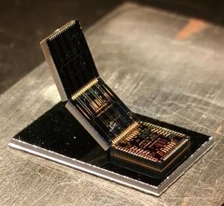
16 3DQP---Orthogonal Integration Daughter Card into Motherboard approach Utilizes standard QP chip for vertical or daughter card elements QP interconnect nodules plug into a socket on MB Applications include system miniaturization, IMU, power electronics & VCSEL integration Technology demonstration currently underway 16
17 3DQP---Orthogonal Integration Demonstration/Progress 17


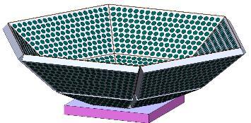
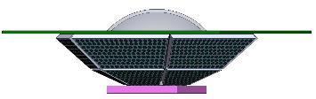
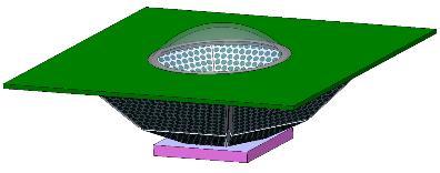
18 3DQP---Alternative Geometries Unique chip shapes can be fabricated due to singulation of wafer by etching QP interconnect nodules enable multiple approaches for I/O, mechanical strength and angle variation Application primarily for curved imaging arrays and conformal structures Technology demonstration currently underway 18

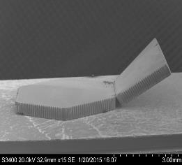

19 3DQP Alternative Geometries Demonstration/Progress 19

20 3DQP Alternative Geometries Electrical Test Demonstrator 20
 QP interconnect nodule requires very little")

21 3DQP---QP + Stacking Integration of QP with TSV (barrel & filled vias) QP interconnect nodule requires very little keep-out area from vias Best of All Worlds approach decreases tradeoffs Applications include large format arrays, system minaturization 21
22 Summary of Quilt Packaging Benefits Optimized integration of disparate materials and process technologies (Si, GaAs, GaN, SiGe, AlN, more) Enables new 3D system architectures beyond just stacking Chip partitioning for optimal yield/functionality Sub-micron chip-to-chip alignment (FPAs, IRSPs, Optical) Better thermal management due to all chips on heatsink Reduced power dissipation, die size, design cycle time Variety of interconnect geometries & sizes available simultaneously Increased IP flexibility, security & design re-use Complementary with existing packaging approaches---can be combined w/tsv, WB, bumping, etc. 22


23 Thank You! IIC works with customers or collaborators on specific applications of QP technology RF/microwave Power Electronics Optical & optoelectronics High Performance Computing MEMs integration in 3D Mechanisms for Collaboration Development Engineering for QP Joint proposals Contract R&D CONTACT: Jason Kulick
Quilt Packaging For Power Electronics
 Quilt Packaging For Power Electronics 21 March 2013 Jason M. Kulick President, Co-Founder Indiana Integrated Circuits, LLC Overview Introduction Quilt Packaging (QP) technology Concept Examples Advantages
Quilt Packaging Microchip Interconnect Technology
 Quilt Packaging Microchip Interconnect Technology 18 November 2012 Jason M. Kulick President, Co-Founder Indiana Integrated Circuits, LLC Overview Introduction to IIC Quilt Packaging (QP) Concept Electrical
3D SYSTEM INTEGRATION TECHNOLOGY CHOICES AND CHALLENGE ERIC BEYNE, ANTONIO LA MANNA
 3D SYSTEM INTEGRATION TECHNOLOGY CHOICES AND CHALLENGE ERIC BEYNE, ANTONIO LA MANNA OUTLINE 3D Application Drivers and Roadmap 3D Stacked-IC Technology 3D System-on-Chip: Fine grain partitioning Conclusion
Challenges of Integration of Complex FHE Systems. Nancy Stoffel GE Global Research
 Challenges of Integration of Complex FHE Systems Nancy Stoffel GE Global Research Products drive requirements to sub-systems, components and electronics GE PRODUCTS CTQs: SWaP, $$, operating environment,
Comparison & highlight on the last 3D TSV technologies trends Romain Fraux
 Comparison & highlight on the last 3D TSV technologies trends Romain Fraux Advanced Packaging & MEMS Project Manager European 3D Summit 18 20 January, 2016 Outline About System Plus Consulting 2015 3D
From 3D Toolbox to 3D Integration: Examples of Successful 3D Applicative Demonstrators N.Sillon. CEA. All rights reserved
 From 3D Toolbox to 3D Integration: Examples of Successful 3D Applicative Demonstrators N.Sillon Agenda Introduction 2,5D: Silicon Interposer 3DIC: Wide I/O Memory-On-Logic 3D Packaging: X-Ray sensor Conclusion
Bringing 3D Integration to Packaging Mainstream
 Bringing 3D Integration to Packaging Mainstream Enabling a Microelectronic World MEPTEC Nov 2012 Choon Lee Technology HQ, Amkor Highlighted TSV in Packaging TSMC reveals plan for 3DIC design based on silicon
Comparison of Singulation Techniques
 Comparison of Singulation Techniques Electronic Packaging Society, Silicon Valley Chapter Sept. 28, 2017 ANNETTE TENG Sept 28, 2017 1 Definition of Singulation 9/28/2017 Annetteteng@promex-ind.com 2 www.cpmt.org/scv
3D Integration & Packaging Challenges with through-silicon-vias (TSV)
") NSF Workshop 2/02/2012 3D Integration & Packaging Challenges with through-silicon-vias (TSV) Dr John U. Knickerbocker IBM - T.J. Watson Research, New York, USA Substrate IBM Research Acknowledgements IBM
NSF Workshop 2/02/2012 3D Integration & Packaging Challenges with through-silicon-vias (TSV) Dr John U. Knickerbocker IBM - T.J. Watson Research, New York, USA Substrate IBM Research Acknowledgements IBM
EECS 598: Integrating Emerging Technologies with Computer Architecture. Lecture 10: Three-Dimensional (3D) Integration
 Integration") 1 EECS 598: Integrating Emerging Technologies with Computer Architecture Lecture 10: Three-Dimensional (3D) Integration Instructor: Ron Dreslinski Winter 2016 University of Michigan 1 1 1 Announcements
1 EECS 598: Integrating Emerging Technologies with Computer Architecture Lecture 10: Three-Dimensional (3D) Integration Instructor: Ron Dreslinski Winter 2016 University of Michigan 1 1 1 Announcements
Vertical Circuits. Small Footprint Stacked Die Package and HVM Supply Chain Readiness. November 10, Marc Robinson Vertical Circuits, Inc
 Small Footprint Stacked Die Package and HVM Supply Chain Readiness Marc Robinson Vertical Circuits, Inc November 10, 2011 Vertical Circuits Building Blocks for 3D Interconnects Infrastructure Readiness
Applications, Processing and Integration Options for High Dielectric Constant Multi-Layer Thin-Film Barium Strontium Titanate (BST) Capacitors
 Capacitors") Applications, Processing and Integration Options for High Dielectric Constant Multi-Layer Thin-Film Barium Strontium Titanate (BST) Capacitors Agenda Introduction What is BST? Unique Characteristics of
Applications, Processing and Integration Options for High Dielectric Constant Multi-Layer Thin-Film Barium Strontium Titanate (BST) Capacitors Agenda Introduction What is BST? Unique Characteristics of
Packaging for parallel optical interconnects with on-chip optical access
 Packaging for parallel optical interconnects with on-chip optical access I. INTRODUCTION Parallel optical interconnects requires the integration of lasers and detectors directly on the CMOS chip. In the
Multi-Die Packaging How Ready Are We?
 Multi-Die Packaging How Ready Are We? Rich Rice ASE Group April 23 rd, 2015 Agenda ASE Brief Integration Drivers Multi-Chip Packaging 2.5D / 3D / SiP / SiM Design / Co-Design Challenges: an OSAT Perspective
TechSearch International, Inc.
 On the Road to 3D ICs: Markets and Solutions E. Jan Vardaman President TechSearch International, Inc. www.techsearchinc.com High future cost of lithography Severe interconnect delay Noted in ITRS roadmap
3D systems-on-chip. A clever partitioning of circuits to improve area, cost, power and performance. The 3D technology landscape
 Edition April 2017 Semiconductor technology & processing 3D systems-on-chip A clever partitioning of circuits to improve area, cost, power and performance. In recent years, the technology of 3D integration
SMAFTI Package Technology Features Wide-Band and Large-Capacity Memory
 SMAFTI Package Technology Features Wide-Band and Large-Capacity Memory KURITA Yoichiro, SOEJIMA Koji, KAWANO Masaya Abstract and NEC Corporation have jointly developed an ultra-compact system-in-package
Rethinking the Hierarchy of Electronic Interconnections. Joseph Fjelstad Verdant Electronics
 Rethinking the Hierarchy of Electronic Interconnections Joseph Fjelstad Verdant Electronics The Industry s Terminology Challenge» The electronics industry continues to explore and develop new methods to
BRIDGING THE GLOBE WITH INNOVATIVE TECHNOLOGY
 BRIDGING THE GLOBE WITH INNOVATIVE TECHNOLOGY Semiconductor Link Processing & Ultra-Thin Semi Wafer Dicing Louis Vintro VP & General Manager, Semiconductor Products Division Semiconductor Link Processing
Introduction 1. GENERAL TRENDS. 1. The technology scale down DEEP SUBMICRON CMOS DESIGN
 1 Introduction The evolution of integrated circuit (IC) fabrication techniques is a unique fact in the history of modern industry. The improvements in terms of speed, density and cost have kept constant
NORTH CORPORATION. Development of IC Packaging Components Enabling Increasing Product Functionality
 NORTH CORPORATION Development of IC Packaging Components Enabling Increasing Product Functionality I. Bump Interconnection (NMBI) Business PWB technology shift toward increased circuit layer count and
DEPARTMENT WAFER LEVEL SYSTEM INTEGRATION
 FRAUNHOFER INSTITUTE FOR RELIABILITY AND MICROINTEGRATION IZM DEPARTMENT WAFER LEVEL SYSTEM INTEGRATION ALL SILICON SYSTEM INTEGRATION DRESDEN ASSID ALL SILICON SYSTEM INTEGRATION DRESDEN FRAUNHOFER IZM-ASSID
AIM Photonics: Manufacturing Challenges for Photonic Integrated Circuits
 AIM Photonics: Manufacturing Challenges for Photonic Integrated Circuits November 16, 2017 Michael Liehr Industry Driving Force EXA FLOP SCALE SYSTEM Blades SiPh Interconnect Network Memory Stack HP HyperX
AT&S Company. Presentation. 3D Component Packaging. in Organic Substrate. Embedded Component. Mark Beesley IPC Apex 2012, San Diego.
 3D Component Packaging AT&S Company in Organic Substrate Presentation Embedded Component Mark Beesley IPC Apex 2012, San Diego www.ats.net Austria Technologie & Systemtechnik Aktiengesellschaft Fabriksgasse13
Functional Testing of 0.3mm pitch Wafer Level Packages to Multi- GHz Speed made possible by Innovative Socket Technology
 Functional Testing of 0.3mm pitch Wafer Level Packages to Multi- GHz Speed made possible by Innovative Socket Technology Ila Pal - Ironwood Electronics Introduction Today s electronic packages have high
TechSearch International, Inc.
 Alternatives on the Road to 3D TSV E. Jan Vardaman President TechSearch International, Inc. www.techsearchinc.com Everyone Wants to Have 3D ICs 3D IC solves interconnect delay problem bandwidth bottleneck
3D technology for Advanced Medical Devices Applications
 3D technology for Advanced Medical Devices Applications By, Dr Pascal Couderc,Jerome Noiray, Dr Christian Val, Dr Nadia Boulay IMAPS MEDICAL WORKSHOP DECEMBER 4 & 5,2012 P.COUDERC 3D technology for Advanced
IBM 43E7488 POWER6 Microprocessor from the IBM System 8203-E4A Server
 43E7488 from the IBM System 8203-E4A Server Package Analysis For comments, questions, or more information about this report, or for any additional technical needs concerning semiconductor technology, please
Kimberly Reid, PhD Director Research Technology
 Kimberly Reid, PhD Director Research Technology Kimberly.Reid@ucf.edu The world s first industry-led consortium (501.c.6 non-profit) for the manufacturing of smart sensors New Era of International Industry
Interconnect Challenges in a Many Core Compute Environment. Jerry Bautista, PhD Gen Mgr, New Business Initiatives Intel, Tech and Manuf Grp
 Interconnect Challenges in a Many Core Compute Environment Jerry Bautista, PhD Gen Mgr, New Business Initiatives Intel, Tech and Manuf Grp Agenda Microprocessor general trends Implications Tradeoffs Summary
Innovative 3D Structures Utilizing Wafer Level Fan-Out Technology
 Innovative 3D Structures Utilizing Wafer Level Fan-Out Technology JinYoung Khim #, Curtis Zwenger *, YoonJoo Khim #, SeWoong Cha #, SeungJae Lee #, JinHan Kim # # Amkor Technology Korea 280-8, 2-ga, Sungsu-dong,
Non-contact Test at Advanced Process Nodes
 Chris Sellathamby, J. Hintzke, B. Moore, S. Slupsky Scanimetrics Inc. Non-contact Test at Advanced Process Nodes June 8-11, 8 2008 San Diego, CA USA Overview Advanced CMOS nodes are a challenge for wafer
IMEC CORE CMOS P. MARCHAL
 APPLICATIONS & 3D TECHNOLOGY IMEC CORE CMOS P. MARCHAL OUTLINE What is important to spec 3D technology How to set specs for the different applications - Mobile consumer - Memory - High performance Conclusions
TechSearch International, Inc.
 Silicon Interposers: Ghost of the Past or a New Opportunity? Linda C. Matthew TechSearch International, Inc. www.techsearchinc.com Outline History of Silicon Carriers Thin film on silicon examples Multichip
Package (1C) Young Won Lim 3/13/13
 Young Won Lim 3/13/13") Copyright (c) 2011-2013 Young W. Lim. Permission is granted to copy, distribute and/or modify this document under the terms of the GNU Free Documentation License, Version 1.2 or any later version published
Copyright (c) 2011-2013 Young W. Lim. Permission is granted to copy, distribute and/or modify this document under the terms of the GNU Free Documentation License, Version 1.2 or any later version published
Burn-in & Test Socket Workshop
 Burn-in & Test Socket Workshop IEEE March 4-7, 2001 Hilton Mesa Pavilion Hotel Mesa, Arizona IEEE COMPUTER SOCIETY Sponsored By The IEEE Computer Society Test Technology Technical Council COPYRIGHT NOTICE
LEVERAGING THE COMMERCIAL SECTOR AND PROVIDING DIFFERENTIATION THROUGH FUNCTIONAL DISAGGREGATION
 LEVERAGING THE COMMERCIAL SECTOR AND PROVIDING DIFFERENTIATION THROUGH FUNCTIONAL DISAGGREGATION Dr. Daniel S. Green, DARPA/MTO Program Manager NDIA Trusted Microelectronics Workshop August 17, 2016 The
Ultra Fine Pitch RDL Development in Multi-layer ewlb (embedded Wafer Level BGA) Packages
 Packages") Ultra Fine Pitch RDL Development in Multi-layer ewlb (embedded Wafer Level BGA) Packages Won Kyoung Choi*, Duk Ju Na*, Kyaw Oo Aung*, Andy Yong*, Jaesik Lee**, Urmi Ray**, Riko Radojcic**, Bernard Adams***
Ultra Fine Pitch RDL Development in Multi-layer ewlb (embedded Wafer Level BGA) Packages Won Kyoung Choi*, Duk Ju Na*, Kyaw Oo Aung*, Andy Yong*, Jaesik Lee**, Urmi Ray**, Riko Radojcic**, Bernard Adams***
Imaging, BiCMOS ASIC and Silicon Photonics. Eric Aussedat Executive Vice President General Manager, Imaging, Bi-CMOS ASIC and Silicon Photonics Group
 Imaging, BiCMOS ASIC and Silicon Photonics Eric Aussedat Executive Vice President General Manager, Imaging, Bi-CMOS ASIC and Silicon Photonics Group IBP Leading Position Targets 2 Image Sensors Solutions
Packaging Innovation for our Application Driven World
 Packaging Innovation for our Application Driven World Rich Rice ASE Group March 14 th, 2018 MEPTEC / IMAPS Luncheon Series 1 What We ll Cover Semiconductor Roadmap Drivers Package Development Thrusts Collaboration
SFP (Small Form-factor Pluggable) Products
 Products") SFP (Small Form-factor Pluggable) Products As a founding member and innovator for the Small Form-factor Pluggable (SFP) Multi-Source Agreement (MSA), Tyco Electronics supports the market with a full range
SFP (Small Form-factor Pluggable) Products As a founding member and innovator for the Small Form-factor Pluggable (SFP) Multi-Source Agreement (MSA), Tyco Electronics supports the market with a full range
Monolithic 3D Integration using Standard Fab & Standard Transistors. Zvi Or-Bach CEO MonolithIC 3D Inc.
 Monolithic 3D Integration using Standard Fab & Standard Transistors Zvi Or-Bach CEO MonolithIC 3D Inc. 3D Integration Through Silicon Via ( TSV ), Monolithic Increase integration Reduce interconnect total
New Era of Panel Based Technology for Packaging, and Potential of Glass. Shin Takahashi Technology Development General Division Electronics Company
 New Era of Panel Based Technology for Packaging, and Potential of Glass Shin Takahashi Technology Development General Division Electronics Company Connecting the World Connecting the World Smart Mobility
Custom Connectors Overview
 Company Overview March 12, 2015 Custom Connectors Overview Tuesday, October 03, 2017 CONNECTOR OVERVIEW Engineering Manufacturing Connector Products HiLo FlexFrame Custom Connectors Standard Connectors
Stacked Silicon Interconnect Technology (SSIT)
") Stacked Silicon Interconnect Technology (SSIT) Suresh Ramalingam Xilinx Inc. MEPTEC, January 12, 2011 Agenda Background and Motivation Stacked Silicon Interconnect Technology Summary Background and Motivation
Stacked Silicon Interconnect Technology (SSIT) Suresh Ramalingam Xilinx Inc. MEPTEC, January 12, 2011 Agenda Background and Motivation Stacked Silicon Interconnect Technology Summary Background and Motivation
Micron Level Placement Accuracy for Wafer Scale Packaging of P-Side Down Lasers in Optoelectronic Products
 Micron Level Placement Accuracy for Wafer Scale Packaging of P-Side Down Lasers in Optoelectronic Products Daniel D. Evans, Jr. and Zeger Bok Palomar Technologies, Inc. 2728 Loker Avenue West Carlsbad,
Package (1C) Young Won Lim 3/20/13
 Young Won Lim 3/20/13") Copyright (c) 2011-2013 Young W. Lim. Permission is granted to copy, distribute and/or modify this document under the terms of the GNU Free Documentation License, Version 1.2 or any later version published
Copyright (c) 2011-2013 Young W. Lim. Permission is granted to copy, distribute and/or modify this document under the terms of the GNU Free Documentation License, Version 1.2 or any later version published
Lockheed Martin Nanosystems
 Lockheed Martin Nanosystems National Nanotechnology Initiative at Ten: Nanotechnology Innovation Summit December 2010 Dr. Brent M. Segal Director & Chief Technologist, LM Nanosystems brent.m.segal@lmco.com
3-D Package Integration Enabling Technologies
 3-D Package Integration Enabling Technologies Nanium - Semi Networking Day David Clark - Choon Heung Lee - Ron Huemoeller June 27th, 2013 Enabling a Microelectronic World Mobile Communications Driving
Wafer Level Packaging The Promise Evolves Dr. Thomas Di Stefano Centipede Systems, Inc. IWLPC 2008
 Wafer Level Packaging The Promise Evolves Dr. Thomas Di Stefano Centipede Systems, Inc. IWLPC 2008 / DEVICE 1.E+03 1.E+02 1.E+01 1.E+00 1.E-01 1.E-02 1.E-03 1.E-04 1.E-05 1.E-06 1.E-07 Productivity Gains
Packaging Technology for Image-Processing LSI
 Packaging Technology for Image-Processing LSI Yoshiyuki Yoneda Kouichi Nakamura The main function of a semiconductor package is to reliably transmit electric signals from minute electrode pads formed on
Photonics Integration in Si P Platform May 27 th Fiber to the Chip
 Photonics Integration in Si P Platform May 27 th 2014 Fiber to the Chip Overview Introduction & Goal of Silicon Photonics Silicon Photonics Technology Wafer Level Optical Test Integration with Electronics
THERMAL EXPLORATION AND SIGN-OFF ANALYSIS FOR ADVANCED 3D INTEGRATION
 THERMAL EXPLORATION AND SIGN-OFF ANALYSIS FOR ADVANCED 3D INTEGRATION Cristiano Santos 1, Pascal Vivet 1, Lee Wang 2, Michael White 2, Alexandre Arriordaz 3 DAC Designer Track 2017 Pascal Vivet Jun/2017
Ultra-thin Capacitors for Enabling Miniaturized IoT Applications
 Ultra-thin Capacitors for Enabling Miniaturized IoT Applications Fraunhofer Demo Day, Oct 8 th, 2015 Konrad Seidel, Fraunhofer IPMS-CNT 10/15/2015 1 CONTENT Why we need thin passive devices? Integration
3D Power Electronics Packaging and Additive Manufacturing
 3D Power Electronics Packaging and Additive Manufacturing Presented by Dr. Doug Hopkins NCSU DCHopkins@NCSU.edu www..org 2015 Douglas C Hopkins Packaging v. Manufacturing PACKAGING: a Design Process MANUFACTURING:
SI2 Technologies, Inc.
 SI2 Technologies, Inc. Flexible, Printed Electronics for Sensing and Energy Storage imaps Workshop May 5, 2015 ISO-9001:2008 Certified Quality Management System Erik S. Handy, Ph.D. Principal Scientist
OEpic s Business Presentation
 OEpic s Business Presentation 10-40Gb/s InP OEICs OEpic, Inc. Sunnyvale, California June, 2001 OEpic s Vision Advanced EO / OE Integration Integrate the Best of Optical Components With Millimeter Wave
TLS-Dicing for concentrator dies - a fast and clean technology. Hans-Ulrich Zühlke
 TLS-Dicing for concentrator dies - a fast and clean technology Hans-Ulrich Zühlke TLS-Dicing with JENOPTIK-VOTAN Semi Contents Overview Jenoptik Principle of TLS-Technology TLS-Dicing the benefits at a
MicraGEM-Si A flexible process platform for complex MEMS devices
 MicraGEM-Si A flexible process platform for complex MEMS devices By Dean Spicer, Jared Crawford, Collin Twanow, and Nick Wakefield Introduction MicraGEM-Si is a process platform for MEMS prototyping and
,M,R,!iilll""M,:3 MEMS. ~ IliJctanill:5 Pac~ RSI. YSTEMS
 ,M,R,!iilll""M,:3 U!i!.,TIRAw.'";P,RElCISIONI,F'LEXIBLE W,I!:IIR:I;C,ICELL, MEMS ~ IliJctanill:5 Pac~.... RSI. YSTEMS ULTRA-PRECISION flexible ASSEMBLY WORK CELL Turnkey production for: MEMS Multi-Chip
PRODUCTION OF ULTRA-FLAT SEMICONDUCTOR WAFER SUBSTRATES USING ADVANCED OPTICAL LENS POLISHING TECHNOLOGY
 PRODUCTION OF ULTRA-FLAT SEMICONDUCTOR WAFER SUBSTRATES USING ADVANCED OPTICAL LENS POLISHING TECHNOLOGY / Slide 1 IQBAL (IZZY) BANSAL ASML HOLDING (NV) iqbalbansal@asml.com JANUARY 10, 2009
High-bandwidth CX4 optical connector
 High-bandwidth CX4 optical connector Dubravko I. Babić, Avner Badihi, Sylvie Rockman XLoom Communications, 11 Derech Hashalom, Tel-Aviv, Israel 67892 Abstract We report on the development of a 20-GBaud
Advanced CSP & Turnkey Solutions. Fumio Ohyama Tera Probe, Inc.
 Advanced CSP & Turnkey Solutions Fumio Ohyama Tera Probe, Inc. Tera Probe - Corporate Overview 1. Company : Tera Probe, Inc. 2. Founded : August, 2005 3. Capital : Approx. USD118.2 million (as of March
SFP (Small Form-factor Pluggable) Products
 Products") SFP (Small Form-factor Pluggable) Products As a founding member and innovator for the Small Form-factor Pluggable (SFP) Multi-Source Agreement (MSA), TE supports the market with a full range of SFP products.
SFP (Small Form-factor Pluggable) Products As a founding member and innovator for the Small Form-factor Pluggable (SFP) Multi-Source Agreement (MSA), TE supports the market with a full range of SFP products.
CMP Model Application in RC and Timing Extraction Flow
 INVENTIVE CMP Model Application in RC and Timing Extraction Flow Hongmei Liao*, Li Song +, Nickhil Jakadtar +, Taber Smith + * Qualcomm Inc. San Diego, CA 92121 + Cadence Design Systems, Inc. San Jose,
Embedded UTCP interposers for miniature smart sensors
 Embedded UTCP interposers for miniature smart sensors T. Sterken 1,2, M. Op de Beeck 2, Tom Torfs 2, F. Vermeiren 1,2, C. Van Hoof 2, J. Vanfleteren 1,2 1 CMST (affiliated with Ugent and IMEC), Technologiepark
Test and Measurement Challenges for 3D IC Development. R. Robertazzi IBM Research
 Test and Measurement Challenges for 3D IC Development R. Robertazzi IBM Research PFA Bill Price. Pete Sorce. John Ott. David Abraham. Pavan Samudrala Digital Test Kevin Stawaisz. TEL P12 Prober Glen Lansman,
Advanced Wafer Level Technology: Enabling Innovations in Mobile, IoT and Wearable Electronics
 Advanced Wafer Level Technology: Enabling Innovations in Mobile, IoT and Wearable Electronics Seung Wook Yoon, *Boris Petrov, **Kai Liu STATS ChipPAC Ltd. 10 #04-08/09 Techpoint Singapore 569059 *STATS
ZEISS Launches New High-resolution 3D X-ray Imaging Solutions for Advanced Semiconductor Packaging Failure Analysis
 Press Release ZEISS Launches New High-resolution 3D X-ray Imaging Solutions for Advanced Semiconductor Packaging Failure Analysis New submicron and nanoscale XRM systems and new microct system provide
Power Consumption in 65 nm FPGAs
 White Paper: Virtex-5 FPGAs R WP246 (v1.2) February 1, 2007 Power Consumption in 65 nm FPGAs By: Derek Curd With the introduction of the Virtex -5 family, Xilinx is once again leading the charge to deliver
MARKET PERSPECTIVE: SEMICONDUCTOR TREND OF 2.5D/3D IC WITH OPTICAL INTERFACES PHILIPPE ABSIL, IMEC
 MARKET PERSPECTIVE: SEMICONDUCTOR TREND OF 2.5D/3D IC WITH OPTICAL INTERFACES PHILIPPE ABSIL, IMEC OUTLINE Market Trends & Technology Needs Silicon Photonics Technology Remaining Key Challenges Conclusion
A Fine Pitch MEMS Probe Card with Built in Active Device for 3D IC Test
 3000.0 2500.0 2000.0 1500.0 1000.0 500.0 0.00-500.0-1000.0-1500.0 OSCILLOSCOPE Design file: MSFT DIFF CLOCK WITH TERMINATORREV2.FFS Designer: Microsoft HyperLynx V8.0 Comment: 650MHz at clk input, J10,
There is a paradigm shift in semiconductor industry towards 2.5D and 3D integration of heterogeneous parts to build complex systems.
 Direct Connection and Testing of TSV and Microbump Devices using NanoPierce Contactor for 3D-IC Integration There is a paradigm shift in semiconductor industry towards 2.5D and 3D integration of heterogeneous
CMOS SENSOR SYSTEM FOR AIR QUALITY MONITORING
 European Network on New Sensing Technologies for Air Pollution Control and Environmental Sustainability - TD1105 INTERNATIONAL WG1-EuNetAir COST Action WG4 MEETING on New Sensing Technologies and Modelling
Interposer Technology: Past, Now, and Future
 Interposer Technology: Past, Now, and Future Shang Y. Hou TSMC 侯上勇 3D TSV: Have We Waited Long Enough? Garrou (2014): A Little More Patience Required for 2.5/3D All things come to those who wait In 2016,
Emerging IC Packaging Platforms for ICT Systems - MEPTEC, IMAPS and SEMI Bay Area Luncheon Presentation
 Emerging IC Packaging Platforms for ICT Systems - MEPTEC, IMAPS and SEMI Bay Area Luncheon Presentation Dr. Li Li Distinguished Engineer June 28, 2016 Outline Evolution of Internet The Promise of Internet
LITHOGRAPHY CHALLENGES FOR LEADING EDGE 3D PACKAGING APPLICATIONS
 LITHOGRAPHY CHALLENGES FOR LEADING EDGE 3D PACKAGING APPLICATIONS Warren W. Flack, Manish Ranjan, Gareth Kenyon, Robert Hsieh Ultratech, Inc. 3050 Zanker Road, San Jose, CA 95134 USA mranjan@ultratech.com
Wire Bonding Solutions for Complex Memory Packages. John Foley Kulicke & Soffa Industries
 Wire Bonding Solutions for Complex Memory Packages John Foley Kulicke & Soffa Industries Growth in the Memory Market Segment DRAM Unit Shipment Forecast (M units) By Density 2014 2015 2016 2017 2018 2019
Ultra Thin Substrate Assembly Challenges for Advanced Flip Chip Package
 Ultra Thin Substrate Assembly Challenges for Advanced Flip Chip Package by Fred Lee*, Jianjun Li*, Bindu Gurram* Nokibul Islam, Phong Vu, KeonTaek Kang**, HangChul Choi** STATS ChipPAC, Inc. *Broadcom
Process Design Kit for for Flexible Hybrid Electronics (FHE-PDK)
") Process Design Kit for for Flexible Hybrid Electronics (FHE-PDK) Tsung-Ching Jim Huang, PhD Sr. Research Scientist, Hewlett Packard Labs MEPTEC2018 Outline Introduction Modeling and design needs for flexible
Process Design Kit for for Flexible Hybrid Electronics (FHE-PDK) Tsung-Ching Jim Huang, PhD Sr. Research Scientist, Hewlett Packard Labs MEPTEC2018 Outline Introduction Modeling and design needs for flexible
Packaging and Integration Technologies for Silicon Photonics. Dr. Peter O Brien, Tyndall National Institute, Ireland.
 Packaging and Integration Technologies for Silicon Photonics Dr. Peter O Brien, Tyndall National Institute, Ireland. Opportunities for Silicon Photonics Stress Sensors Active Optical Cable 300 mm Silicon
inemi Roadmap and Technical Plan on Organic PCB Bill Bader, inemi inemi PCB/Laminate Workshop, Taipei October 22, 2013
 inemi Roadmap and Technical Plan on Organic PCB Bill Bader, inemi inemi PCB/Laminate Workshop, Taipei October 22, 2013 Agenda inemi Roadmap Process and Scope 2013 PCB Roadmap and TIG Outcomes Summary &
WLSI Extends Si Processing and Supports Moore s Law. Douglas Yu TSMC R&D,
 WLSI Extends Si Processing and Supports Moore s Law Douglas Yu TSMC R&D, chyu@tsmc.com SiP Summit, Semicon Taiwan, Taipei, Taiwan, Sep. 9 th, 2016 Introduction Moore s Law Challenges Heterogeneous Integration
inemi Roadmap Packaging and Component Substrates TWG
 inemi Roadmap Packaging and Component Substrates TWG TWG Leaders: W. R. Bottoms William Chen Presented by M. Tsuriya Agenda Situation Everywhere in Electronics Evolution & Blooming Drivers Changing inemi
High Performance Electronics Integration in Flexible Technology
 High Performance Electronics Integration in Flexible Technology February 10, 2011 www.americansemi.com 2011 American Semiconductor, Inc. All rights reserved. About American Semiconductor Corporate Headquarters
Transforming a Leading-Edge Microprocessor Wafer Fab into a World Class Silicon Foundry. Dr. Thomas de Paly
 Transforming a Leading-Edge Microprocessor Wafer Fab into a World Class Silicon Foundry Dr. Thomas de Paly October 06, 2009 Opportunity Meets Vision Vision To be the first truly global semiconductor foundry,
Cantilever Based Ultra Fine Pitch Probing
 Cantilever Based Ultra Fine Pitch Probing Christian Leth Petersen Peter Folmer Nielsen Dirch Petersen SouthWest Test Workshop San Diego, June 2004 1 About CAPRES Danish MEMS probe & interfacing venture
FOUNDRY SERVICES. RF & mm-wave Applications. 1GHz 2GHz 5GHz 10GHz 20GHz 50GHz 100GHz
 FOUNDRY SERVICES UMS has developed a proven family of GaAs based processes for high performance low noise and high power MMICs. These processes are extensively used by foundry customers and by UMS to offer
Verification of Singulated HBM2 stacks with Die Level Handler. Dave Armstrong Toshiyuki Kiyokawa Quay Nhin
 Verification of Singulated HBM2 stacks with Die Level Handler Dave Armstrong Toshiyuki Kiyokawa Quay Nhin Abstract Background only will delete on final material High-Bandwidth-Memory continues to evolve
Safe Harbor Statement
 May 2017 1 Safe Harbor Statement Matters discussed in this presentation may contain forward-looking statements that are subject to risks and uncertainties. These risks and uncertainties could cause the
Technology & Manufacturing. Laurent Bosson Executive Vice President Front End Technology & Manufacturing
 Technology & Manufacturing Laurent Bosson Executive Vice President Front End Technology & Manufacturing Manufacturing and Technology Strategy LEADING EDGE TECHNOLOGY + SHAREHOLDER VALUE TIME TO MARKET
Advancing high performance heterogeneous integration through die stacking
 Advancing high performance heterogeneous integration through die stacking Suresh Ramalingam Senior Director, Advanced Packaging European 3D TSV Summit Jan 22 23, 2013 The First Wave of 3D ICs Perfecting
SECTION 1 IMP / UMP R107
 1 SECTION 1 / UMP R107 Contents Introduction... 1-4 to 1-6 Characteristics...1-7 Board to board connectors...1-8 Receptacle packaging...1-9 Assembly instructions... 1-9 to 1-10 UMP Characteristics...1-11
Key Considerations to Probe Cu Pillars in High Volume Production
 Key Considerations to Probe Cu Pillars in High Volume Production Alexander Wittig (GLOBALFOUNDRIES) Amy Leong, Tin Nguyen, Tommaso Masi, Jarek Kister, Mike Slessor (Form Factor) Overview Key Industry Trends
LEVERAGING THE COMMERCIAL SECTOR AND PROVIDING DIFFERENTIATION THROUGH FUNCTIONAL DISAGGREGATION
 LEVERAGING THE COMMERCIAL SECTOR AND PROVIDING DIFFERENTIATION THROUGH FUNCTIONAL DISAGGREGATION Dr. Daniel S. Green, DARPA/MTO Program Manager The DARPA solution is to provide a menu of hardware security
ACCURACY, SPEED, RELIABILITY. Turnkey Production for: MEMS. Multi-Chip Modules. Semiconductor Packaging. Microwave Modules.
 >> Turnkey Production for: MEMS Multi-Chip Modules Semiconductor Packaging Microwave Modules Flip Chip Photonics Packaging ACCURACY, SPEED, RELIABILITY ULTRA-PRECISION ASSEMBLY WORK CELL Turnkey production
Collaboration for Breakthrough Innovation in Human Performance Monitoring for the Warfighter
 Collaboration for Breakthrough Innovation in Human Performance Monitoring for the Warfighter NDIA 2018 Human Systems Conference Dr. Melissa Grupen-Shemansky Chief Technology Officer, SEMI / FlexTech megshemansky@semi.org
For personal use only
 2016 BluGlass Investor Presentation GILES BOURNE MANAGING DIRECTOR CORPORATE OVERVIEW BOARD George Venardos Chairman Giles Bourne Managing Director CORPORATE Established 2006 TOP SHAREHOLDERS as at 1 Aug.
Introducing the FX-14 ASIC Design System. Embargoed until November 10, 2015
 Introducing the FX-14 ASIC Design System Embargoed until November 10, 2015 Market Forces Are Driving Need for a New Breed of Semiconductor By 2019: Bandwidth Roughly one million minutes of video will cross
Thermal Sign-Off Analysis for Advanced 3D IC Integration
 Sign-Off Analysis for Advanced 3D IC Integration Dr. John Parry, CEng. Senior Industry Manager Mechanical Analysis Division May 27, 2018 Topics n Acknowledgements n Challenges n Issues with Existing Solutions