A STUDY OF DESIGN TOOL - XILINX
|
|
|
- Shanna Stanley
- 6 years ago
- Views:
Transcription


1 A STUDY OF DESIGN TOOL - XILINX 1. Open Xilinx Project Navigator from Start Menu Xilinx ISE Opens-up 2. Opening a New ProjectSelect New Project from File Menu The below window opensup Enter the Project Name -> Click Next 1

2 3. Enter the device details as follows - > Click Next 4. Click on New Source Tab 2

3 5. Select Verilog Module and Enter a name for the module Click Next 6. Define the Input and Output Port for the module being designed 3

4 7. Finish the Yes 8. Click Next Next Finish. The new Project opens-up in the ISE - IDE 9. Enter the program Code Save the file Select Check Syntax by collapsing Synthesize XST 4


5 10. Once Check Syntax is Successful Simulate the design using ModelSim Change the source for dropdown to Behavioral Simulation To Create TestBench Select the project from Sources window Right Click Select New Source 11. Select Test Bench Waveform and give a file name for the testbench being created Click Next Verify the Association Next Finish 5


6 12. Select Combinational or Sequential as per the simulation and enter the clock details 13. Assigning Values to input and output 6


7 14. Entering Values 15. Save the test bench & Select Simulate Behavioral model from processes window by collapsing ModelSim Simulator. The Simulated output for the testbench being created appears in ModelSim 7


8 Check Syntax & Synthesis User Constraint ->Floorplan I/O -> Click YES 8


9 Enter PIN Details-> SAVE Click OK RUN IMPLEMENT DesignRUN Generate Program file RUN Configure Target device Manage configuration project IMPACT Window opens up 9


10 After Clicking Finish ->Assign New Configuration File Dialog Opens up Click Bypass After Clicking Bypass ->Assign New Configuration File Dialog Opens up Select bit file Click open 10

11 In below dialog - > Select Apply Click OK Right Click the second IC and select Program 11


12 Click on Apply OK Check the output in KIT 12
13 SUMMARY Check Syntax &Behavioral Simulation Synthesis User Constraint ->Floorplan I/O -> Click YES Enter PIN Details-> SAVE Click OK RUN IMPLEMENT Design RUN Generate Program file Configure Target device Manage configuration project 13
14 CIRCUIT DIAGRAM LOGIC GATES AND ITS TRUTH TABLES 14
15 Ex.No: 1 LOGIC GATES AIM: To design Logic gates using Verilog HDL, verify its function by simulating in Xilinx APPARATUS REQUIRED: 1. Xilinx ISE 8.1i 2. ModelSim SE Plus 5.7g 3. XC3S400 FPGA Kit, Manual 4. Power Supply PROCEDURE 1. Write and draw the Digital logic system. 2. Write the Verilog code for above system. 3. Enter the Verilog code in Xilinx software. 4. Check the syntax and simulate the above Verilog code (using ModelSim or Xilinx) and 5. Verify the output waveform as obtained. 15
16 SIMULATION OUTPUT: ANDGATE 16
17 VERILOG CODE: STRUCTURAL MODELLING moduleandgate (i1, i2,out); input i1, i2; output out; and (out,i1,i2); TESTBENCH moduletestandgate; // Inputs reg i1; reg i2; // Outputs wire out; // Instantiate the Unit Under Test (UUT) Andgateuut (.i1(i1),.i2(i2),.out(out) ); initial begin // Initialize Inputs i1 = 0; i2 = 0; // Wait 100 ns for global reset to finish #100; // Add stimulus here #100 i1=1'b1; i2=1'b0; #100 i1=1'b0; i2=1'b1; #100 i1=1'b1; i2=1'b1; end 17
18 OR- GATE 18
19 VERILOG CODE STRUCTURAL MODELLING moduleorgate (i1, i2,out); input i1, i2; output out; or (out,i1,i2); TESTBENCH module testor; // Inputs reg i1; reg i2; // Outputs wire out; // Instantiate the Unit Under Test (UUT) Orgate uut (.i1(i1),.i2(i2),.out(out) ); initial begin // Initialize Inputs i1 = 0; i2 = 0; // Wait 100 ns for global reset to finish #100; // Add stimulus here #100 i1=1'b1; i2=1'b0; #100 i1=1'b0; i2=1'b1; #100 i1=1'b1; i2=1'b1; end 19
20 NAND GATE 20
21 VERILOG CODE DATAFLOW MODELLING modulenandgate (i1, i2,out); input i1, i2; output out; assign out = ~ ( i1 & i2); TESTBENCH moduletestnand; // Inputs reg i1; reg i2; // Outputs wire out; // Instantiate the Unit Under Test (UUT) Nandgateuut (.i1(i1),.i2(i2),.out(out) ); initial begin // Initialize Inputs i1 = 0; i2 = 0; // Wait 100 ns for global reset to finish #100; // Add stimulus here #100 i1=1'b1; i2=1'b0; #100 i1=1'b0; i2=1'b1; #100 i1=1'b1; i2=1'b1; end 21
22 XOR GATE 22
23 VERILOG CODE DATAFLOW MODELLING modulexorgate ( i1,out); input i1; output out; assign out = ( i1 ^ i2); TESTBENCH moduletestxor; // Inputs reg i1; reg i2; // Outputs wire out; // Instantiate the Unit Under Test (UUT) Xorgateuut (.i1(i1),.i2(i2),.out(out) ); initial begin // Initialize Inputs i1 = 0; i2 = 0; // Wait 100 ns for global reset to finish #100; // Add stimulus here #100 i1=1'b1; i2=1'b0; #100 i1=1'b0; i2=1'b1; #100 i1=1'b1; i2=1'b1; end RESULT: Thus the various logic gates were designed and corresponding outputs verified. 23

24 CIRCUIT DIAGRAM HALF ADDER: FULL ADDER 24
25 Ex.No:2 ADDERS AIM: To design half adder and full adder using Verilog HDL, verify its function by simulating in Xilinx APPARATUS REQUIRED: 1. Xilinx ISE 8.1i 2. ModelSim SE Plus 5.7g 3. XC3S400 FPGA Kit, Manual 4. Power Supply PROCEDURE 1. Write and draw the Digital logic system. 2. Write the Verilog code for above system. 3. Enter the Verilog code in Xilinx software. 4. Check the syntax and simulate the above Verilog code (using ModelSim or Xilinx) and 5. Verify the output waveform as obtained. 25
26 SIMULATION OUTPUT: HALFADDER 26
27 VERILOG CODE: HALF ADDER Structural: module ha(sum,c_out,i1,i2); input i1,i2; outputsum,c_out; xor (sum,i1,i2); and (c_out,i1,i2); Dataflow: module ha(s,c,a,b); inputa,b; outputs,c; assign s = a ^ b; assign c = a & b; TESTBENCH moduletestha; // Inputs reg a; reg b; // Outputs wire s; wire c; // Instantiate the Unit Under Test (UUT) hauut (.s(s),.c(c),.a(a),.b(b) ); initial begin // Initialize Inputs a = 0; b = 0; // Wait 100 ns for global reset to finish #100; // Add stimulus here #100 a=1'b1; b=1'b0; #100 a=1'b0; b=1'b1; #100 a=1'b1; b=1'b1; end 27
28 SIMULATION OUTPUT: FULL ADDER 28
29 FULL ADDER Structural : modulefull_adder_structural(i1,i2, c_in, sum, c_out); input i1,i2c_in; output sum, c_out; wire s1, c1, c2, c3; xor xor_s1(s1, i1, i2); // compute sum. xor xor_s2(sum, s1, c_in); and and_c1(c1, i1,i2); // compute carry out. and and_c2(c2, i1, c_in); and and_c3(c3, i2, c_in); oror_cout(c_out, c1, c2, c3); Dataflow modulefull_adder_structural(x, y, c_in, s, c_out); input x, y, c_in; output s, c_out; assign s = x ^ y ^ z; // compute sum. assignc_out = (a&b) (b&c) (c&a); // compute carry out. TESTBENCH moduletestfa; // Inputs reg i1; reg i2; regc_in; // Outputs wiresum;wirec_out; // Instantiate the Unit Under Test (UUT) full_adder_structuraluut (.i1(i1),.i2(i2),.c_in(c_in),.sum(sum),.c_out(c_out)); initial begin // Initialize Inputs i1 = 0; i2 = 0; c_in = 0; // Wait 100 ns for global reset to finish #100; // Add stimulus here #100i1 = 0;i2 = 0;c_in = 0; #100 i1 = 0;i2 = 0;c_in = 0; #100 i1 = 0;i2 = 0;c_in = 1; 29
30 30
31 end #100 i1 = 0;i2 = 1;c_in = 0; #100 i1 = 0;i2 = 1;c_in = 1; #100 i1 = 1;i2 = 0;c_in = 0; #100 i1 = 1;i2 = 0;c_in = 1; #100 i1 = 1;i2 = 1;c_in = 0; #100 i1 = 1;i2 = 1;c_in = 1; #200 $stop; RESULT: Thus the design and implementation of adders is performed using Verilog HDL and Xilinx tool 31

32 CIRCUIT DIAGRAM HALF SUBTRACTORTRUTH TABLE I1 I2 BR DIFF FULL SUBTRACTORTRUTH TABLE I1 I2 CIN BR DIFF
33 Ex.No:3 SUBTRACTORS AIM: To design a half subtractor and full subtractor using Verilog HDL, verify its function, by simulating in Xilinx APPARATUS REQUIRED: 1. Xilinx ISE 8.1i 2. ModelSim SE Plus 5.7g 3. XC3S400 FPGA Kit, Manual 4. Power Supply PROCEDURE 1. Write and draw the Digital logic system. 2. Write the Verilog code for above system. 3. Enter the Verilog code in Xilinx software. 4. Check the syntax and simulate the above Verilog code (using ModelSim or Xilinx) and 5. Verify the output waveform as obtained. 33
34 SIMULATION OUTPUT: HALF SUBTRACTOR 34
35 VERILOG CODE - HALF SUBTRACTOR STRUCTURAL modulehalf_sub(i1,i2,dif,bor); outputdif,bor; input i1,i2; wire w; xor (dif,i1,i2); not(w,i1); and(bor,w,i2); DATAFLOW module half_subtractor (i1,i2,dif,bor ); output dif ; output bor ; input i1,i2 ; assign dif = i1 ^ i2; assign bor = (~i1) &i2; TESTBENCH moduletesths; // Inputs reg i1; reg i2; // Outputs wiredif; wirebor; // Instantiate the Unit Under Test (UUT) half_subtractoruut (.i1(i1),.i2(i2),.dif(dif),.bor(bor)); initial begin // Initialize Inputs i1 = 0; i2 = 0; // Wait 100 ns for global reset to finish #100; // Add stimulus here i1=1'b0; i2=1'b0; #100 i2=1'b1; #100 i1=1'b1; i2=1'b0; #100 i1=1'b1; i2=1'b1; #100 $stop; end 35
36 SIMULATION OUTPUT: FULL SUBTRACTOR 36
37 VERILOG CODE - FULL SUBTRACTOR STRUCTURAL modulefull_sub(i1,i2,b_in,dif,b_out); outputdif,b_out; input i1,i2,b_in; wire w,w1,w2,w3; xor(dif,i1,i2,b_in); not(w,i1); and(w1,i2,b_in); and(w2,i2,w); and(w3,b_in,w); or(b_out,w1,w2,w3); DATAFLOW module full_subtractor ( i1,i2,b_in,dif,b_out ); output dif; output b_out ; input i1,i2,b_in; assign diff = i1 ^ i2 ^ b_in; assign borrow = ((~i1) &i2) (i2&b_in) (b_in& (~i1)); TEST BENCH moduletestfs; // Inputs reg i1; reg i2; regb_in; // Outputs wiredif;wireb_out; // Instantiate the Unit Under Test (UUT) full_subtractoruut (.i1(i1),.i2(i2),.b_in(b_in),.dif(dif),.b_out(b_out)); initial begin // Initialize Inputs i1 = 0; i2 = 0; b_in = 0; // Wait 100 ns for global reset to finish #100; // Add stimulus here #100 b_in = 0;i1 = 0;i2 = 0; #100 b_in = 0;i1 = 0;i2 = 0; #100 b_in = 0;i1 = 0;i2 = 1; #100 b_in = 0;i1 = 1;i2 = 0; 37
38 38
39 #100 b_in = 0;i1 = 1;i2 = 1; #100 b_in = 1;i1 = 0;i2 = 0; #100 b_in = 1;i1 = 0;i2 = 1; #100 b_in = 1;i1 = 1;i2 = 0; #100 b_in = 1;i1 = 1;i2 = 1; end RESULT Thus the design and implementation of subtractors is performed and results verified using Verilog HDL. 39
 TRUTH TABLE")
40 CIRCUIT DIAGRAM MULTIPLEXER (4X1)TRUTH TABLE DEMULTIPLEXER (1X4) TRUTH TABLE 40
41 Ex.No:4 MULTIPLEXER AND DEMULTIPLEXER AIM: To design a 4X1 multiplexer and Demultiplexer using Verilog HDL, verify its function, by simulating in Xilinx APPARATUS REQUIRED: 1. Xilinx ISE 8.1i 2. ModelSim SE Plus 5.7g 3. XC3S400 FPGA Kit, Manual 4. Power Supply PROCEDURE 1. Write and draw the Digital logic system. 2. Write the Verilog code for above system. 3. Enter the Verilog code in Xilinx software. 4. Check the syntax and simulate the above Verilog code (using ModelSim or Xilinx) and 5. Verify the output waveform as obtained. 41
42 SIMULATION OUTPUT: MULTIPLEXER 42
43 VERILOG CODE: - MULTIPLEXER STRUCTURAL module Mux4to1(i0, i1, i2, i3, s0, s1, out); input i0, i1, i2, i3, s0, s1; output out; wire s1n,s0n; wire y0,y1,y2,y3; not (s1n,s1); not (s0n,s0); and (y0,i0,s1n,s0n); and (y1,i1,s1n,s0); and (y2,i2,s1,s0n); and (y3,i3,s1,s0); or (out,y0,y1,y2,y3); DATAFLOW module multiplexer4_1 ( din,sel,dout ); output dout ; input [3:0] din ; input [1:0] sel ; assign dout = (sel==2'b00)? din[3] : (sel==2'b01)? din[2] : (sel==2'b10)? din[1] : din[0]; BEHAVIOURAL module mux4(mux_out, data_3,data_2, data_1, data_0,select,enable); output [3:0] mux_out; input [3:0] data_3,data_2,data_1,data_0; input [1:0] select; input enable; reg [3:0] mux_int; assignmux_out=enable? mux_int:4'bz; always@(data_3 or data_2 or data_1 or data_0 or select) case(select) 0: mux_int=data_0; 1: mux_int=data_1; 2: mux_int=data_2; 3: mux_int=data_3; default:mux_int=4'bx; //May execute in simulation endcase 43
44 44
45 TEST BENCH moduletestmux; // Inputs reg [3:0] data_3; reg [3:0] data_2; reg [3:0] data_1; reg [3:0] data_0; reg [1:0] select; reg enable; // Outputs wire [3:0] mux_out; // Instantiate the Unit Under Test (UUT) mux4uut (.mux_out(mux_out),.data_3(data_3),.data_2(data_2),.data_0(data_0),.select(select),.enable(enable));.data_1(data_1), initial begin // Initialize Inputs data_3 = 0;data_2 = 0;data_1 = 0;data_0 = 0;select = 0;enable = 0; // Wait 100 ns for global reset to finish #100; // Add stimulus here enable = 1; data_3 = 4'b1010; data_2 = 4'b1000; data_1 = 4'b1100; data_0 = 4'b0110; #100 select= 2'b00; #100 select= 2'b01; #100 select= 2'b10; #100 select= 2'b11; #1 $stop; end 45
46 SIMULATION OUTPUT: DEMULTIPLEXER 46
47 DEMULTIPLEXER STRUCTURAL module Dux1to4(in, s0, s1, out0, out1, out2, out3); input in, s0, s1; output out0, out1, out2,out3; wire s0n,s1n; not(s0n,s0); not(s1n,s1); and (out0,in,s1n,s0n); and (out1,in,s1n,s0); and (out2,in,s1,s0n); and (out3,in,s1,s0); DATAFLOW module demultiplexer4_1 ( din,sel,dout ); output [3:0] dout ; input din ; input [1:0] sel ; assign dout[3] = (sel==2'b00)? din : 1'b0; assign dout[2] = (sel==2'b01)? din : 1'b0; assign dout[1] = (sel==2'b10)? din : 1'b0; assign dout[0] = (sel==2'b11)? din : 1'b0; BEHAVIOURAL module 1x4demux(input wire a, //inputs declaration input wire[1:0] sel, outputreg y1, //outputs declaration outputreg y2, outputreg y3, outputreg y4); //logic for 1x4demux always@(sel or a) case(sel) 2 b00:begin y1=a;y2=1 b0;y3=1 b0;y4=1 b0; end 2 b01:begin y1=1 b0;y2=a;y3=1 b0;y4=1 b0; end 2 b10:begin y1=1 b0;y2=1 b0;y3=a;y4=1 b0; end 2 b11:begin 47
48 48
49 y1=1 b0;y2=1 b0;y3=1 b0;y4=a; end endcase TESTBENCH moduletestdemux; // Inputs reg din;reg [1:0] sel; // Outputs wire [3:0] dout; // Instantiate the Unit Under Test (UUT) demultiplexer4_1uut (.din(din),.sel(sel),.dout(dout)); initial begin // Initialize Inputs din = 0;sel = 0; // Wait 100 ns for global reset to finish #100; // Add stimulus here din = 1; #100 sel= 2'b00; #100 sel= 2'b01; #100 sel= 2'b10; #100 sel= 2'b11; end RESULT Thus a 4x1 Multiplexer and Demultiplexerare designed using Verilog HDL and its functioning is verified 49


50 CIRCUIT DIAGRAM ENCODER DECODER 50
51 Ex.No:5 ENCODER AND DECODER AIM To design an encoder and decoder using Verilog HDL, verify their function, by simulating in Xilinx APPARATUS REQUIRED: 1. Xilinx ISE 8.1i 2. ModelSim SE Plus 5.7g 3. XC3S400 FPGA Kit, Manual 4. Power Supply PROCEDURE 1. Write and draw the Digital logic system. 2. Write the Verilog code for above system. 3. Enter the Verilog code in Xilinx software. 4. Check the syntax and simulate the above Verilog code (using ModelSim or Xilinx) and 5. Verify the output waveform as obtained. 51
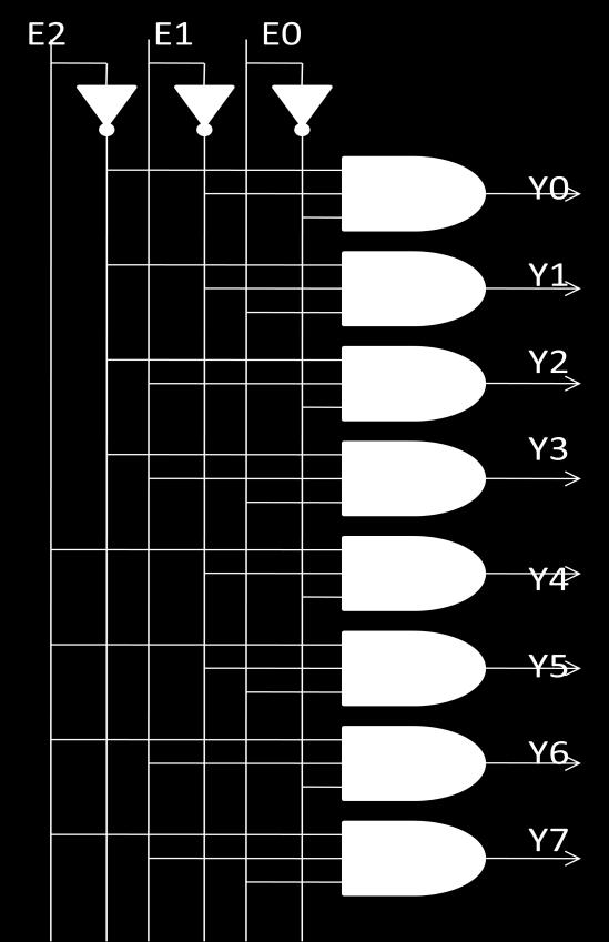
52 ENCODER TRUTH TABLE INPUTS OUTPUT Y7 Y6 Y5 Y4 Y3 Y2 Y1 Y0 E0 E1 E SIMULATION OUTPUT 52
53 VERILOG CODE: - ENCODER Structural Module encoder_structural(y0,y1,y2,y3,y4,y5,y6,y7, e0,e1,e2); input y0,y1,y2,y3,y4,y5,y6,y7; output e0,e1,e2; wire w1,w2,w3,w4,w5,w6; or or1(w1, y7, y6); or or2(w2,y5,y4); or or3(e0,w1,w2); or or4(w3, y7, y6); or or5(w4,y3,y2); or or6(e1,w3,w4); or or7(w5, y7, y5); or or8(w6,y1,y3); or or9(e2,w5,w6); Dataflow Module encoder_behavioral(y0,y1,y2,y3,y4,y5,y6,y7, e0,e1,e2); input y0,y1,y2,y3,y4,y5,y6,y7; output e0,e1,e2; assign e0 = (y7 y6 y5 y4); assign e1 = (y7 y6 y3 y2); assign e2 = (y7 y5 y3 y1); Behavioral Module encoder_4to2_behavioral(y0,y1,y2,y3, e0,e1); input y0,y1,y2,y3,y4; output e0,e1; if (y0 ==1 & y1 == 0 & y2 ==0 & y3== 0) then begin e0=0; e1=0; end else if (y0 ==0 & y1 == 1 & y2 ==0 & y3== 0) then begin e0=1; e1=0; end else if(y0 ==1 & y1 == 0 & y2 ==0 & y3== 0); begin e0=0; e1=1; end else begin e0=1; e1=1; end endif 53
54 54
55 TESTBENCH moduletestentt; // Inputs reg y0, y1, y2, y3; // Outputs wire e0, e1; // Instantiate the Unit Under Test (UUT) encoder_behavioraluut (.y0(y0),.y1(y1),.y2(y2),.y3(y3),..e0(e0),.e1(e1)); initial begin // Initialize Inputs y0 = 0; y1 = 0; y2 = 0; y3 = 0; // Wait 100 ns for global reset to finish #100; // Add stimulus here y0 = 1;y1 = 0; y2 = 0;y3 = 0; #100 y0 = 0;y1 = 1; y2 = 0;y3 = 0; end 55
56 DECODER TRUTH TABLE INPUTS E0 E1 E OUTPUTS Y7 Y6 Y5 Y4 Y3 Y2 Y1 Y SIMULATION OUTPUT: 56
57 DECODER moduledec(data, Code); output [7:0] Data; input [2:0] Code; reg [7:0] Data; (Code) begin if(code==0) Data=8'b ;else if(code==1) Data=8'b ;else if(code==2) Data=8'b ;else if(code==3) Data=8'b ;else if(code==4) Data=8'b ;else if(code==5) Data=8'b ;else if(code==6) Data=8'b ;else if(code==7) Data=8'b ;else Data=8'bx; end RESULT: Thus an encoder and decoder are designed using Verilog HDL and its functioning is verified 57
58 CIRCUIT DIAGRAM D-FLIP FLOPS EXCITATION TABLE SET RESET D CLK Q Qbar rising rising 0 1 JK-FLIP FLOPS EXCITATION TABLE J K Q(t+1) 0 0 Q(t) no change 0 1 0(reset to 0) 1 0 1(set to 1) 1 1 Qbar(t) 58
59 Ex.No:6 FLIP FLOPS AIM: To design the basic sequential element flipflopusing Verilog HDL, verify its function, by simulating in Xilinx APPARATUS REQUIRED: 1. Xilinx ISE 8.1i 2. ModelSim SE Plus 5.7g 3. XC3S400 FPGA Kit, Manual 4. Power Supply PROCEDURE 1. Write and draw the Digital logic system. 2. Write the Verilog code for above system. 3. Enter the Verilog code in Xilinx software. 4. Check the syntax and simulate the above Verilog code (using ModelSim or Xilinx) and 5. verify the output waveform as obtained. 59
60 SIMULATION OUTPUT: D-FLIPFLOP 60
61 VERILOG CODE: D- FLIPFLOP moduled_ff( q,d,clock,reset); output q; inputd,clock,reset; reg q; Clock or negedge Reset) if (Reset == 0) q<=1'b0; else q<=d; TESTBENCH moduletestdff; // Inputs reg d; reg Clock; reg Reset; // Outputs wire q; // Instantiate the Unit Under Test (UUT) D_ffuut (.q(q),.d(d),.clock(clock),.reset(reset) ); initial begin // Initialize Inputs d = 0; Clock = 0; Reset = 0; // Wait 100 ns for global reset to finish #100; // Add stimulus here #50 Reset=0;d=1; #50 d=0; #50 Reset=1; d=1; #50 d=0; #50 d=1; #50 Reset=0; d=0; #50; // Gap for display. #50 $stop; end always #50 Clock = ~Clock; 61
62 SIMULATION OUTPUT: JK FLIPFLOP 62
63 JK FLIPFLOP modulejkflop(j,k,clk,rst,q); inputj,k,clk,rst;output q;reg q; or posedgerst)begin if (rst == 1) begin q <= 0; end else if(j==1 & k==1 &rst==0)begin q <=~q; //Toggles end else if(j==1 & k==0 &rst==0)begin q <= 1; //Set end else if(j==0 & k==1)begin q <= 0; //Cleared end end TESTBENCH moduletestjk; reg j; reg k; regclk;regrst;wire q; // Instantiate the Unit Under Test (UUT) jkflopuut (.j(j),.k(k),.clk(clk),.rst(rst),.q(q)); initial begin // Initialize Inputs j = 0;k = 0;clk = 0;rst = 1; // Wait 100 ns for global reset to finish #100; // Add stimulus here #2 j=0; k=1; #2 j=1; k=0; #2 j=1; k=1; #2 rst=0;j=0; k=0; #2 j=0; k=1; #2 j=1; k=0; #2 j=1; k=1; #2 rst=1; j=0; k=0; #1; #2 $stop;end always #1 clk=~clk; RESULT Thus, the sequential elements D-Flipflop, JK Flipflop were designed implemented and their outputs verified. 63
64 CIRCUIT DIAGRAM 2-BIT COUNTER 64
65 Ex.No:7A 2_BIT COUNTER AIM: To design a 2 bit counter using Verilog HDL, verify its function, by simulating in Xilinx APPARATUS REQUIRED: 1. Xilinx ISE 8.1i 2. ModelSim SE Plus 5.7g 3. XC3S400 FPGA Kit, Manual 4. Power Supply PROCEDURE 1. Write and draw the Digital logic system. 2. Write the Verilog code for above system. 3. Enter the Verilog code in Xilinx software. 4. Check the syntax and simulate the above Verilog code (using ModelSim or Xilinx) and 5. Verify the output waveform as obtained. 65
66 SIMULATION OUTPUT 2 BIT COUNTER 66
67 VERILOG CODE module Count2Bit(Clock, Clear, out); input Clock, Clear; output [1:0] out; reg [1:0]out; Clock, negedge Clear) if((~clear) (out>=4)) out=2'b00; else out=out+1; TEST BENCH moduletestcount; // Inputs regclock;reg Clear; // Outputs wire [1:0] out; // Instantiate the Unit Under Test (UUT) Count2Bit uut (.Clock(Clock),.Clear(Clear),.out(out)); initial begin // Initialize Inputs Clock = 0;Clear = 0; // Wait 100 ns for global reset to finish #100; // Add stimulus here #10 Clear=1; #18 Clear=0; #2 $stop; end always #1 Clock=~Clock; RESULT Thus a 2 bit counter is designed using Verilog HDL and its functioning is verified using Xilinx tool. 67

68 CIRCUIT DIAGRAM: UP-DOWN COUNTER 68
69 Ex.No:7B UP/DOWN COUNTER AIM: To design an up/down counter using Verilog HDL, verify its function, by simulating in Xilinx. APPARATUS REQUIRED: 1. Xilinx ISE 8.1i 2. ModelSim SE Plus 5.7g 3. XC3S400 FPGA Kit, Manual 4. Power Supply PROCEDURE 1. Write and draw the Digital logic system. 2. Write the Verilog code for above system. 3. Enter the Verilog code in Xilinx software. 4. Check the syntax and simulate the above Verilog code (using ModelSim or Xilinx) and 5. verify the output waveform as obtained. 69
70 SIMULATION OUTPUT 70
71 VERILOG CODE: module count1(count, up_dwn, clock, reset_); output [2:0] count; input [1:0] up_dwn; input clock,reset_; reg [2:0] count; clock or negedge reset_) if(reset_ == 0) count <= 3'b0;else if(up_dwn == 2'b00 up_dwn == 2'b11) count<=count; else if(up_dwn == 2'b01) count<=count+1;else if(up_dwn == 2'b10) count<=count-1; TESTBENCH moduletestudcount; // Inputs reg [1:0] up_dwn; reg clock; reg reset_; // Outputs wire [2:0] count; // Instantiate the Unit Under Test (UUT) count1uut (.count(count),.up_dwn(up_dwn),.clock(clock),.reset_(reset_) ); initial begin // Initialize Inputs up_dwn = 0; clock = 0; reset_ = 0; // Wait 100 ns for global reset to finish #100; // Add stimulus here reset_=0; #30 reset_=1; up_dwn = 2'b01; #10 up_dwn = 2'b00; #10 up_dwn = 2'b10; #10 up_dwn = 2'b11; #10 reset_=0; #2 $stop; end always #1 clock=~clock; RESULT: Thus a Up-Down counter is designed using Verilog HDL and its functions verified in Xilinx and FPGA Kit. 71
72 CIRCUIT DIAGRAM MOD 7 COUNTER 72
73 Ex.No:7C MOD 7 COUNTER AIM Xilinx To design a mod 7 counter using Verilog HDL, verify its function, by simulating in APPARATUS REQUIRED: 1. Xilinx ISE 8.1i 2. ModelSim SE Plus 5.7g 3. XC3S400 FPGA Kit, Manual 4. Power Supply PROCEDURE 1. Write and draw the Digital logic system. 2. Write the Verilog code for above system. 3. Enter the Verilog code in Xilinx software. 4. Check the syntax and simulate the above Verilog code (using ModelSim or Xilinx) and 5. Verify the output waveform as obtained. 73
74 SIMULATION OUTPUT 74
75 VERILOG CODE module counter_mod7 ( clk,reset,dout ); output [2:0] dout ; reg [2:0] dout ; inputclk ;wire clk ;input reset ;wire reset ; initialdout = 0; (posedge (clk)) begin if (reset) dout<= 0; else if (dout<6) dout<= dout + 1; else dout<= 0; end TESTBENCH module testmod7; // Inputs regclk;reg reset; // Outputs wire [2:0] dout; // Instantiate the Unit Under Test (UUT) counter_mod7uut (.clk(clk),.reset(reset),.dout(dout)); initial begin // Initialize Inputs clk = 0;reset = 0; // Wait 100 ns for global reset to finish #100; // Add stimulus here reset =1; #10 reset = 0; #100 $stop; end always #1 clk=~clk; RESULT Thus a Mod 7 counter is designed using verilog HDL and verified in FPGA after implementation with the help of Xilinx. 75
76 CIRCUIT DIAGRAM SHIFT REGISTERS - SIPO SHIFT REGISTERS PISO 76
77 Ex.No:8 SHIFT REGISTER AIM To design a SIPO and PISO shift register using Verilog HDL, verify its function, by simulating in Xilinx APPARATUS REQUIRED: 1. Xilinx ISE 8.1i 2. ModelSim SE Plus 5.7g 3. XC3S400 FPGA Kit, Manual 4. Power Supply PROCEDURE 1. Write and draw the Digital logic system. 2. Write the Verilog code for above system. 3. Enter the Verilog code in Xilinx software. 4. Check the syntax and simulate the above Verilog code (using ModelSim or Xilinx) and 5. Verify the output waveform as obtained. 77
78 SIMULATION OUTPUT SIPO 78
79 VERILOG CODE: SIPO module SIPO ( din,clk,reset,dout ); output [3:0] dout ;wire [3:0] dout ; inputdin,clk,reset; wiredin,clk,reset; reg [3:0]s; (posedge (clk)) begin if (reset) s <= 0; else begin s[3] <= din; s[2] <= s[3]; s[1] <= s[2]; s[0] <= s[1]; end end assigndout = s; TESTBENCH moduletestsipo; // Inputs reg din;regclk;reg reset; // Outputs wire [3:0] dout; // Instantiate the Unit Under Test (UUT) SIPO uut (.din(din),.clk(clk),.reset(reset),.dout(dout)); initial begin // Initialize Inputs din = 0;clk = 0;reset = 0; // Wait 100 ns for global reset to finish #100; // Add stimulus here reset = 1; #100 reset =0 ;din=1; #10 din = 0; #10 din = 1; #20 din = 1; end always #1 clk = ~clk; 79
80 SIMULATION OUTPUT PISO 80
81 PISO moduleparallel_in_serial_out ( din,clk,reset,load,dout ); outputdout ;regdout ; input [3:0] din ;input clk,reset,load ; wire [3:0] din ;wire clk,reset,load ; reg [3:0]temp; (posedge (clk)) begin if (reset) temp<= 1; else if (load) temp<= din; else begin dout<= temp[3]; temp<= {temp[2:0],1'b0}; end end TESTBENCH moduletestpiso; // Inputs reg [3:0] din; regclk, reset, load; // Outputs wiredout; // Instantiate the Unit Under Test (UUT) parallel_in_serial_outuut (.din(din),.clk(clk),.reset(reset),.load(load),.dout(dout)); initial begin // Initialize Inputs din = 0;clk = 0;reset = 0;load = 0; // Wait 100 ns for global reset to finish #100; // Add stimulus here reset=1; #10 reset = 0; #10 load = 1; din=4'b1000; #10 load = 0; end always #1 clk = ~clk; RESULTS Thus SISO and PISO shift registers are designed using Verilog and functionally verified 81
82 BLOCK DIAGRAM: PRBS GENERATOR ACCUMULATOR : 82
83 Ex.No: 9 PRBS GENERATOR AND ACCUMULATOR AIM To design a PRBS generator and accumulator using Verilog HDL, verify its function, in Xilinx, APPARATUS REQUIRED: 1. Xilinx ISE 8.1i 2. ModelSim SE Plus 5.7g 3. XC3S400 FPGA Kit, Manual 4. Power Supply PROCEDURE 1. Write and draw the Digital logic system. 2. Write the Verilog code for above system. 3. Enter the Verilog code in Xilinx software. 4. Check the syntax and simulate the above Verilog code (using ModelSim or Xilinx) and 5. verify the output waveform as obtained. 83
84 SIMULATION RESULT- ACCUMULATOR 84
85 VERILOG CODE moduleupaccm(clk,reset,q,d); input reset;input clk;input [5:0]d;output reg [5:0]q; //reg [3:0]temp; or negedge reset) begin if(~reset) q=4'b0000; else q=q+d; end //assign q=temp; TESTBENCH moduletestaccum; // Inputs regclk;reg reset;reg [5:0] d; // Outputs wire [5:0] q; // Instantiate the Unit Under Test (UUT) upaccmuut (.clk(clk),.reset(reset),.q(q),.d(d)); initial begin // Initialize Inputs clk = 0; reset = 0; d = 0; // Wait 100 ns for global reset to finish #100; // Add stimulus here reset = 1; # 50 d=4'b0010; #200 reset = 0; #50 reset = 1; end always #50 clk = ~clk; 85
86 SIMULATION OUTPUT- PRBS GENERATOR 86
87 VERILOG CODE: moduleprbsgenerator(rand,clk,reset); inputclk,reset;output rand;wire rand;reg[3:0]temp; reset) temp<=4'hf; begin if(~reset) temp<={temp[0]^temp[1],temp[3],temp[2],temp[1]}; end assign rand=temp[0]; TESTBENCH modulemainprbs; regclk,reset;wire rand; prbsgeneratorpr(rand,clk,reset); initial begin forever begin forever begin clk<=0;#5clk<=1;#5clk<=0; end end end initial begin reset=1;#12reset=0;#90reset=1;#12reset=0; end RESULT: Thus a PRBS Generator and Accumulator are designed using Verilog HDL and verified by simulation in Xiinx and implementation in FPGA. 87
88 BLOCK DIAGRAM RCA ADDER 4BIT 88
89 Ex.No:10A 8 BIT ADDER AIM: To design an 8 bit adder using Verilog HDL, verify its function, by simulating in Xilinx. APPARATUS REQUIRED: 1. Xilinx ISE 8.1i 2. ModelSim SE Plus 5.7g 3. XC3S400 FPGA Kit, Manual 4. Power Supply PROCEDURE 1. Write and draw the Digital logic system. 2. Write the Verilog code for above system. 3. Enter the Verilog code in Xilinx software. 4. Check the syntax and simulate the above Verilog code (using ModelSim or Xilinx) and 5. Verify the output waveform as obtained. 89
90 90
91 VERILOG CODE module add_rca_8(sum,c_out,a,b,c_in); output[7:0] sum; outputc_out; input[7:0] a,b; inputc_in; wire c_in2, c_in3, c_in4, c_in5, c_in6, c_in7,c_in8; Add_fullM1(sum[0],c_in2,a[0],b[0],c_in); Add_fullM2(sum[1],c_in3,a[1],b[1],c_in2); Add_fullM3(sum[2],c_in4,a[2],b[2],c_in3); Add_fullM4(sum[3],c_in5,a[3],b[3],c_in4); Add_fullM5(sum[4],c_in6,a[4],b[4],c_in5); Add_fullM6(sum[5],c_in7,a[5],b[5],c_in6); Add_fullM7(sum[6],c_in8,a[6],b[6],c_in7); Add_fullM8(sum[7],c_out,a[7],b[7],c_in8); moduleadd_full(sum,c_out,a,b,c_in); outputsum,c_out; inputa,b,c_in; wire w1,w2,w3; Add_halfM1(w1,w2,a,b); Add_halfM2(sum,w3,w1,c_in); or M3(c_out,w2,w3); moduleadd_half(sum,c_out,a,b); outputsum,c_out; inputa,b; xor M1(sum,a,b); and M2(c_out,a,b); DATAFLOW module adder(a,b, s,c); input [7:0] a,b; output [7:0] s,c; assign {c,s} = a + b; 91
92 SIMULATION OUTPUT 92
93 TESTBENCH moduletestrca; // Inputs reg [7:0] a;reg [7:0] b; // Outputs wire [7:0] s; wire [7:0] c; // Instantiate the Unit Under Test (UUT) adderuut (.a(a),.b(b),.s(s),.c(c)); initial begin // Initialize Inputs a = 0; b = 0; // Wait 100 ns for global reset to finish #100; // Add stimulus here a=8'b ;b=8'b ; #100 a=8'b ;b=8'b ; end RESULT: Thus a 8 bit adder is designed using Verilog HDL and its functioning is verified in Xilinx and FPGA kit. 93
94 BLOCK DIAGRAM MULTIPLIER 94
95 Ex.No:10B 4 BIT MULTIPLIER AIM: Xilinx To design a 4 bit multiplier using Verilog HDL, verify its function, by simulating in APPARATUS REQUIRED: 1. Xilinx ISE 8.1i 2. ModelSim SE Plus 5.7g 3. XC3S400 FPGA Kit, Manual 4. Power Supply PROCEDURE 1. Write and draw the Digital logic system. 2. Write the Verilog code for above system. 3. Enter the Verilog code in Xilinx software. 4. Check the syntax and simulate the above Verilog code (using ModelSim or Xilinx) and 5. Verify the output waveform as obtained. 95
96 96
97 VERILOG CODE STRUCTURAL module HA(sout,cout,a,b); outputsout,cout; inputa,b; assignsout=a^b; assigncout=(a&b); module FA(sout,cout,a,b,cin); outputsout,cout; inputa,b,cin; assignsout=(a^b^cin); assigncout=((a&b) (a&cin) (b&cin)); module multiply4bits(product,inp1,inp2); output [7:0]product; input [3:0]inp1; input [3:0]inp2; wire x1,x2,x3,x4,x5,x6,x7,x8,x9,x10,x11,x12,x13,x14,x15,x16,x17; assign product[0]=(inp1[0]&inp2[0]); HA HA1(product[1],x1,(inp1[1]&inp2[0]),(inp1[0]&inp2[1])); FA FA1(x2,x3,inp1[1]&inp2[1],(inp1[0]&inp2[2]),x1); FA FA2(x4,x5,(inp1[1]&inp2[2]),(inp1[0]&inp2[3]),x3); HA HA2(x6,x7,(inp1[1]&inp2[3]),x5); HA HA3(product[2],x15,x2,(inp1[2]&inp2[0])); FA FA5(x14,x16,x4,(inp1[2]&inp2[1]),x15); FA FA4(x13,x17,x6,(inp1[2]&inp2[2]),x16); FA FA3(x9,x8,x7,(inp1[2]&inp2[3]),x17); HA HA4(product[3],x12,x14,(inp1[3]&inp2[0])); FA FA8(product[4],x11,x13,(inp1[3]&inp2[1]),x12); FA FA7(product[5],x10,x9,(inp1[3]&inp2[2]),x11); FA FA6(product[6],product[7],x8,(inp1[3]&inp2[3]),x10); 97
98 SIMULATION RESULT 98
99 DATAFLOW module multi(a,b, c); input [3:0] a,b; output [7:0] c; assign c = a * b; TESTBENCH moduletestmulti; // Inputs reg [3:0] a;reg [3:0] b; // Outputs wire [7:0] c; // Instantiate the Unit Under Test (UUT) multiuut (.a(a),.b(b),.c(c)); initial begin // Initialize Inputs a = 0;b = 0; // Wait 100 ns for global reset to finish #100; // Add stimulus here a=4'b0001;b=4'b0010; #100; a=4'b0101;b=4'b0010; end RESULT: Thus a 4 bit multiplier is designed using Verilog HDL and its functioning verified in Xilinx and FPGA kit 99
100 100
Department of Computer Science & Engineering. Lab Manual DIGITAL LAB. Class: 2nd yr, 3rd sem SYLLABUS
 Department of Computer Science & Engineering Lab Manual 435 DIGITAL LAB Class: 2nd yr, 3rd sem SYLLABUS. Verification of Boolean theorems using digital logic gates. 2. Design and implementation of code
 DEPT OF ECE EC6612 -VLSI DESIGN LABORATORY MANUAL (REGULATION-2013) LAB MANUAL DEPARTMENT OF ECE NAME: REGISTER NUMBER: YEAR/SEM.: ACADEMIC YEAR: 2015-2016 DEPT OF ECE EC6612 -VLSI DESIGN LABORATORY MANUAL
FPGA Design Challenge :Techkriti 14 Digital Design using Verilog Part 1
 FPGA Design Challenge :Techkriti 14 Digital Design using Verilog Part 1 Anurag Dwivedi Digital Design : Bottom Up Approach Basic Block - Gates Digital Design : Bottom Up Approach Gates -> Flip Flops Digital
N-input EX-NOR gate. N-output inverter. N-input NOR gate
 Hardware Description Language HDL Introduction HDL is a hardware description language used to design and document electronic systems. HDL allows designers to design at various levels of abstraction. It
DIGITAL SYSTEM DESIGN
 DIGITAL SYSTEM DESIGN Prepared By: Engr. Yousaf Hameed Lab Engineer BASIC ELECTRICAL & DIGITAL SYSTEMS LAB DEPARTMENT OF ELECTRICAL ENGINEERING Digital System Design 1 Name: Registration No: Roll No: Semester:
Dr NNCE ECE/VI-SEM VLSI DESIGN LAB-LM
 EC2357-VLSI DESIGN LABORATORY LABORATORY MANUAL FOR SIXTH SEMESTER B.E (ECE) (FOR PRIVATE CIRCULATION ONLY) ACADEMIC YEAR(2013-2014) ANNA UNIVERSITY, CHENNAI-25 DEPARTMENT OF ELECTRONICS AND COMMUNICATION
Verilog Fundamentals. Shubham Singh. Junior Undergrad. Electrical Engineering
 Verilog Fundamentals Shubham Singh Junior Undergrad. Electrical Engineering VERILOG FUNDAMENTALS HDLs HISTORY HOW FPGA & VERILOG ARE RELATED CODING IN VERILOG HDLs HISTORY HDL HARDWARE DESCRIPTION LANGUAGE
Digital Design with FPGAs. By Neeraj Kulkarni
 Digital Design with FPGAs By Neeraj Kulkarni Some Basic Electronics Basic Elements: Gates: And, Or, Nor, Nand, Xor.. Memory elements: Flip Flops, Registers.. Techniques to design a circuit using basic
Digital Circuit Design and Language. Datapath Design. Chang, Ik Joon Kyunghee University
 Digital Circuit Design and Language Datapath Design Chang, Ik Joon Kyunghee University Typical Synchronous Design + Control Section : Finite State Machine + Data Section: Adder, Multiplier, Shift Register
 PAGE NO: EXP NO: 1A SIMULATION OF HALF ADDER AND FULL ADDER. DATE: AIM: To design, simulate and synthesize the Half adder and Full adder. TOOLS REQUIRED: SOFTWARE: XILINX ISE 9.1i ALGORITHM: 1. Start the
Modeling Sequential Circuits in Verilog
 Modeling Sequential Circuits in Verilog COE 202 Digital Logic Design Dr. Muhamed Mudawar King Fahd University of Petroleum and Minerals Presentation Outline Modeling Latches and Flip-Flops Blocking versus
Chapter 9: Sequential Logic Modules
 Chapter 9: Sequential Logic Modules Prof. Ming-Bo Lin Department of Electronic Engineering National Taiwan University of Science and Technology Digital System Designs and Practices Using Verilog HDL and
Verilog Tutorial (Structure, Test)
") Digital Circuit Design and Language Verilog Tutorial (Structure, Test) Chang, Ik Joon Kyunghee University Hierarchical Design Top-down Design Methodology Bottom-up Design Methodology Module START Example)
Digital Circuit Design and Language Verilog Tutorial (Structure, Test) Chang, Ik Joon Kyunghee University Hierarchical Design Top-down Design Methodology Bottom-up Design Methodology Module START Example)
Chap 6 Introduction to HDL (d)
") Design with Verilog Chap 6 Introduction to HDL (d) Credit to: MD Rizal Othman Faculty of Electrical & Electronics Engineering Universiti Malaysia Pahang Ext: 6036 VERILOG HDL Basic Unit A module Module
Design with Verilog Chap 6 Introduction to HDL (d) Credit to: MD Rizal Othman Faculty of Electrical & Electronics Engineering Universiti Malaysia Pahang Ext: 6036 VERILOG HDL Basic Unit A module Module
Graduate Institute of Electronics Engineering, NTU. FPGA Lab. Speaker : 鍾明翰 (CMH) Advisor: Prof. An-Yeu Wu Date: 2010/12/14 ACCESS IC LAB
 Advisor: Prof. An-Yeu Wu Date: 2010/12/14 ACCESS IC LAB") FPGA Lab Speaker : 鍾明翰 (CMH) Advisor: Prof. An-Yeu Wu Date: 2010/12/14 ACCESS IC LAB Objective In this Lab, you will learn the basic set-up and design methods of implementing your design by ISE 10.1. Create
FPGA Lab Speaker : 鍾明翰 (CMH) Advisor: Prof. An-Yeu Wu Date: 2010/12/14 ACCESS IC LAB Objective In this Lab, you will learn the basic set-up and design methods of implementing your design by ISE 10.1. Create
Synthesis of Combinational and Sequential Circuits with Verilog
 Synthesis of Combinational and Sequential Circuits with Verilog What is Verilog? Hardware description language: Are used to describe digital system in text form Used for modeling, simulation, design Two
ENEE245 Digital Circuits and Systems Lab Manual
 ENEE245 Digital Circuits and Systems Lab Manual Department of Engineering, Physical & Computer Sciences Montgomery College Modified Fall 2017 Copyright Prof. Lan Xiang (Do not distribute without permission)
CSE 591: Advanced Hardware Design and Verification (2012 Spring) LAB #0
 LAB #0") Lab 0: Tutorial on Xilinx Project Navigator & ALDEC s Active-HDL Simulator CSE 591: Advanced Hardware Design and Verification Assigned: 01/05/2011 Due: 01/19/2011 Table of Contents 1 Overview... 2 1.1
Lab 0: Tutorial on Xilinx Project Navigator & ALDEC s Active-HDL Simulator CSE 591: Advanced Hardware Design and Verification Assigned: 01/05/2011 Due: 01/19/2011 Table of Contents 1 Overview... 2 1.1
Digital Logic Design Lab
 Digital Logic Design Lab DEPARTMENT OF ELECTRICAL ENGINEERING LAB BROCHURE DIGITAL LOGIC DESIGN LABORATORY CONTENTS Lab Venue... 3 Lab Objectives & Courses... 3 Lab Description & Experiments... 4 Hardware
Introduction to Verilog HDL. Verilog 1
 Introduction to HDL Hardware Description Language (HDL) High-Level Programming Language Special constructs to model microelectronic circuits Describe the operation of a circuit at various levels of abstraction
Lab 7 (Sections 300, 301 and 302) Prelab: Introduction to Verilog
 Prelab: Introduction to Verilog") Lab 7 (Sections 300, 301 and 302) Prelab: Introduction to Verilog Name: Sign the following statement: On my honor, as an Aggie, I have neither given nor received unauthorized aid on this academic work
Lab 7 (Sections 300, 301 and 302) Prelab: Introduction to Verilog Name: Sign the following statement: On my honor, as an Aggie, I have neither given nor received unauthorized aid on this academic work
ACS College of Engineering. Department of Biomedical Engineering. Logic Design Lab pre lab questions ( ) Cycle-1
 Cycle-1") ACS College of Engineering Department of Biomedical Engineering Logic Design Lab pre lab questions (2015-2016) Cycle-1 1. What is a combinational circuit? 2. What are the various methods of simplifying
ACS College of Engineering Department of Biomedical Engineering Logic Design Lab pre lab questions (2015-2016) Cycle-1 1. What is a combinational circuit? 2. What are the various methods of simplifying
Verilog HDL. Gate-Level Modeling
 Verilog HDL Verilog is a concurrent programming language unlike C, which is sequential in nature. block - executes once at time 0. If there is more then one block, each execute concurrently always block
Hardware Description Languages (HDLs) Verilog
 Verilog") Hardware Description Languages (HDLs) Verilog Material from Mano & Ciletti book By Kurtulus KULLU Ankara University What are HDLs? A Hardware Description Language resembles a programming language specifically
Hardware Description Languages (HDLs) Verilog Material from Mano & Ciletti book By Kurtulus KULLU Ankara University What are HDLs? A Hardware Description Language resembles a programming language specifically
Department of Electrical and Computer Engineering Xilinx ISIM <Release Version: 14.1i> Simulation Tutorial Using Verilog
 Department of Electrical and Computer Engineering Xilinx ISIM Simulation Tutorial Using Verilog Spring 2013 Baback Izadi You will next test the full adder circuit that you built
Logic Circuits II ECE 2411 Thursday 4:45pm-7:20pm. Lecture 3
 Logic Circuits II ECE 2411 Thursday 4:45pm-7:20pm Lecture 3 Lecture 3 Topics Covered: Chapter 4 Discuss Sequential logic Verilog Coding Introduce Sequential coding Further review of Combinational Verilog
What is Verilog HDL? Lecture 1: Verilog HDL Introduction. Basic Design Methodology. What is VHDL? Requirements
 What is Verilog HDL? Lecture 1: Verilog HDL Introduction Verilog Hardware Description Language(HDL)? A high-level computer language can model, represent and simulate digital design Hardware concurrency
Federal Urdu University of Arts, Science and Technology, Islamabad VLSI SYSTEM DESIGN. Prepared By: Engr. Yousaf Hameed.
 VLSI SYSTEM DESIGN Prepared By: Engr. Yousaf Hameed Lab Engineer BASIC ELECTRICAL & DIGITAL SYSTEMS LAB DEPARTMENT OF ELECTRICAL ENGINEERING VLSI System Design 1 LAB 01 Schematic Introduction to DSCH and
Chapter 9: Sequential Logic Modules
 Chapter 9: Sequential Logic Modules Prof. Soo-Ik Chae Digital System Designs and Practices Using Verilog HDL and FPGAs @ 2008, John Wiley 9-1 Objectives After completing this chapter, you will be able
Sequential Logic Blocks
 Sequential Logic Blocks Output of sequential blocks depends on present state as well as on past state. Sequential circuits work with a reference which is clock. A clock signal can be of any duty cycle,
Design Using Verilog
 EGC220 Design Using Verilog Baback Izadi Division of Engineering Programs bai@engr.newpaltz.edu Basic Verilog Lexical Convention Lexical convention are close to C++. Comment // to the of the line. /* to
ENEE245 Digital Circuits and Systems Lab Manual
 ENEE245 Digital Circuits and Systems Lab Manual Department of Engineering, Physical & Computer Sciences Montgomery College Version 1.1 Copyright Prof. Lan Xiang (Do not distribute without permission) 1
Chap 3. Modeling structure & basic concept of Verilog HDL
 Chap 3. Modeling structure & basic concept of Verilog HDL Fall semester, 2016 Prof. Jaeseok Kim School of Electrical & Electronics Eng. Yonsei university jaekim@yonsei.ac.kr Digital System Design 3-1 Chapter
DIGITAL SYSTEM DESIGN
 DIGITAL SYSTEM DESIGN Prepared By: Engr. Yousaf Hameed Lab Engineer BASIC ELECTRICAL & DIGITAL SYSTEMS LAB DEPARTMENT OF ELECTRICAL ENGINEERING Digital System Design 1 Name: Registration No: Roll No: Semester:
Speaker: Shao-Wei Feng Adviser: Prof. An-Yeu Wu Date: 2010/09/28
 99-1 Under-Graduate Project Verilog Simulation & Debugging Tools Speaker: Shao-Wei Feng Adviser: Prof. An-Yeu Wu Date: 2010/09/28 ACCESS IC LAB Outline Basic Concept of Verilog HDL Gate Level Modeling
A Brief Introduction to Verilog Hardware Definition Language (HDL)
") www.realdigital.org A Brief Introduction to Verilog Hardware Definition Language (HDL) Forward Verilog is a Hardware Description language (HDL) that is used to define the structure and/or behavior of digital
www.realdigital.org A Brief Introduction to Verilog Hardware Definition Language (HDL) Forward Verilog is a Hardware Description language (HDL) that is used to define the structure and/or behavior of digital
DEPARTMENT OF COMPUTER SCIENCE AND ENGINEERING LAB MANUAL. Academic Year: ODD SEMESTER
 DEPARTMENT OF COMPUTER SCIENCE AND ENGINEERING LAB MANUAL Academic Year: 25-6 ODD SEMESTER Programme (UG/PG) Semester Course Code Course Title : UG : VII : CS43 : VLSI LAB Prepared By
Nikhil Gupta. FPGA Challenge Takneek 2012
 Nikhil Gupta FPGA Challenge Takneek 2012 RECAP FPGA Field Programmable Gate Array Matrix of logic gates Can be configured in any way by the user Codes for FPGA are executed in parallel Configured using
MLR Institute of Technology
 MLR Institute of Technology Laxma Reddy Avenue, Dundigal, Quthbullapur (M), Hyderabad 500 043 Course Name Course Code Class Branch ELECTRONICS AND COMMUNICATIONS ENGINEERING QUESTION BANK : DIGITAL DESIGN
VERILOG CODES //SPECIAL COMBINATIONAL LOGIC CIRCUITS
 VERILOG CODES //SPECIAL COMBINATIONAL LOGIC CIRCUITS //VERILOG CODE FOR THE IMPLEMENTATION OF HALF ADDER (DATAFLOW MODEL) module half_adder(a, b, sum, cout); input a,b; output sum,cout; assign sum=a ^
Chapter 2 Using Hardware Description Language Verilog. Overview
 Chapter 2 Using Hardware Description Language Verilog CSE4210 Winter 2012 Mokhtar Aboelaze based on slides by Dr. Shoab A. Khan Overview Algorithm development isa usually done in MATLAB, C, or C++ Code
Date Performed: Marks Obtained: /10. Group Members (ID):. Experiment # 11. Introduction to Verilog II Sequential Circuits
:. Experiment # 11. Introduction to Verilog II Sequential Circuits") Name: Instructor: Engr. Date Performed: Marks Obtained: /10 Group Members (ID):. Checked By: Date: Experiment # 11 Introduction to Verilog II Sequential Circuits OBJECTIVES: To understand the concepts
Name: Instructor: Engr. Date Performed: Marks Obtained: /10 Group Members (ID):. Checked By: Date: Experiment # 11 Introduction to Verilog II Sequential Circuits OBJECTIVES: To understand the concepts
Tutorial on Verilog HDL
 Tutorial on Verilog HDL HDL Hardware Description Languages Widely used in logic design Verilog and VHDL Describe hardware using code Document logic functions Simulate logic before building Synthesize code
Lab 6 : Introduction to Verilog
 Lab 6 : Introduction to Verilog Name: Sign the following statement: On my honor, as an Aggie, I have neither given nor received unauthorized aid on this academic work 1 Objective The main objective of
Digital Design (VIMIAA01) Introduction to the Verilog HDL
 Introduction to the Verilog HDL") BUDAPEST UNIVERSITY OF TECHNOLOGY AND ECONOMICS FACULTY OF ELECTRICAL ENGINEERING AND INFORMATICS DEPARTMENT OF MEASUREMENT AND INFORMATION SYSTEMS Digital Design (VIMIAA01) Introduction to the Verilog
BUDAPEST UNIVERSITY OF TECHNOLOGY AND ECONOMICS FACULTY OF ELECTRICAL ENGINEERING AND INFORMATICS DEPARTMENT OF MEASUREMENT AND INFORMATION SYSTEMS Digital Design (VIMIAA01) Introduction to the Verilog
 UNIT II - COMBINATIONAL LOGIC Part A 2 Marks. 1. Define Combinational circuit A combinational circuit consist of logic gates whose outputs at anytime are determined directly from the present combination
VLSI Design 13. Introduction to Verilog
 Last module: Sequential circuit design Design styles This module Synthesis Brief introduction to Verilog Synthesis in the Design Flow Designer Tasks Tools Architect Logic Designer Circuit Designer Define
Hardware Description Language VHDL (1) Introduction
 Introduction") Hardware Description Language VHDL (1) Introduction Digital Radiation Measurement and Spectroscopy NE/RHP 537 Introduction Hardware description language (HDL) Intended to describe circuits textually, for
Hardware Description Language VHDL (1) Introduction Digital Radiation Measurement and Spectroscopy NE/RHP 537 Introduction Hardware description language (HDL) Intended to describe circuits textually, for
Verilog 1 - Fundamentals
 Verilog 1 - Fundamentals FA FA FA FA module adder( input [3:0] A, B, output cout, output [3:0] S ); wire c0, c1, c2; FA fa0( A[0], B[0], 1 b0, c0, S[0] ); FA fa1( A[1], B[1], c0, c1, S[1] ); FA fa2( A[2],
Lab 7 (All Sections) Prelab: Introduction to Verilog
 Prelab: Introduction to Verilog") Lab 7 (All Sections) Prelab: Introduction to Verilog Name: Sign the following statement: On my honor, as an Aggie, I have neither given nor received unauthorized aid on this academic work 1 Objective The
Lab 7 (All Sections) Prelab: Introduction to Verilog Name: Sign the following statement: On my honor, as an Aggie, I have neither given nor received unauthorized aid on this academic work 1 Objective The
Amrita Vishwa Vidyapeetham. EC429 VLSI System Design Answer Key
 Time: Two Hours Amrita Vishwa Vidyapeetham B.Tech Second Assessment March 2013 Eighth Semester Electrical and Electronics Engineering EC429 VLSI System Design Answer Key Answer all Questions Roll No: Maximum:
ECE 4514 Digital Design II. Spring Lecture 2: Hierarchical Design
 ECE 4514 Digital Design II Spring 2007 Abstraction in Hardware Design Remember from last lecture that HDLs offer a textual description of a netlist. Through abstraction in the HDL, we can capture more
EE 8351 Digital Logic Circuits Ms.J.Jayaudhaya, ASP/EEE
 EE 8351 Digital Logic Circuits Ms.J.Jayaudhaya, ASP/EEE 1 Logic circuits for digital systems may be combinational or sequential. A combinational circuit consists of input variables, logic gates, and output
Synthesizable Verilog
 Synthesizable Verilog Courtesy of Dr. Edwards@Columbia, and Dr. Franzon@NCSU http://csce.uark.edu +1 (479) 575-6043 yrpeng@uark.edu Design Methodology Structure and Function (Behavior) of a Design HDL
Introduction to Verilog/System Verilog
 NTUEE DCLAB Feb. 27, 2018 Introduction to Verilog/System Verilog Presenter: Yao-Pin Wang 王耀斌 Advisor: Prof. Chia-Hsiang Yang 楊家驤 Dept. of Electrical Engineering, NTU National Taiwan University What is
Why Should I Learn This Language? VLSI HDL. Verilog-2
 Verilog Why Should I Learn This Language? VLSI HDL Verilog-2 Different Levels of Abstraction Algorithmic the function of the system RTL the data flow the control signals the storage element and clock Gate
The Verilog Language COMS W Prof. Stephen A. Edwards Fall 2002 Columbia University Department of Computer Science
 The Verilog Language COMS W4995-02 Prof. Stephen A. Edwards Fall 2002 Columbia University Department of Computer Science The Verilog Language Originally a modeling language for a very efficient event-driven
Verilog 1 - Fundamentals
 Verilog 1 - Fundamentals FA FA FA FA module adder( input [3:0] A, B, output cout, output [3:0] S ); wire c0, c1, c2; FA fa0( A[0], B[0], 1 b0, c0, S[0] ); FA fa1( A[1], B[1], c0, c1, S[1] ); FA fa2( A[2],
CSCB58 - Lab 3. Prelab /3 Part I (in-lab) /2 Part II (in-lab) /2 TOTAL /8
 /2 Part II (in-lab) /2 TOTAL /8") CSCB58 - Lab 3 Latches, Flip-flops, and Registers Learning Objectives The purpose of this exercise is to investigate the fundamental synchronous logic elements: latches, flip-flops, and registers. Prelab
CSCB58 - Lab 3 Latches, Flip-flops, and Registers Learning Objectives The purpose of this exercise is to investigate the fundamental synchronous logic elements: latches, flip-flops, and registers. Prelab
LABORATORY MANUAL VLSI DESIGN LAB EE-330-F
 LABORATORY MANUAL VLSI DESIGN LAB EE-330-F (VI th Semester) Prepared By: Vikrant Verma B. Tech. (ECE), M. Tech. (ECE) Department of Electrical & Electronics Engineering BRCM College of Engineering & Technology
VALLIAMMAI ENGINEERING COLLEGE. SRM Nagar, Kattankulathur DEPARTMENT OF ELECTRONICS AND COMMUNICATION ENGINEERING EC6302 DIGITAL ELECTRONICS
 VALLIAMMAI ENGINEERING COLLEGE SRM Nagar, Kattankulathur-603 203 DEPARTMENT OF ELECTRONICS AND COMMUNICATION ENGINEERING EC6302 DIGITAL ELECTRONICS YEAR / SEMESTER: II / III ACADEMIC YEAR: 2015-2016 (ODD
Veriolog Overview. CS/EE 3710 Fall 2010
 Veriolog Overview CS/EE 3710 Fall 2010 Hardware Description Languages HDL Designed to be an alternative to schematics for describing hardware systems Two main survivors VHDL Commissioned by DOD Based on
Post-Synthesis Simulation. VITAL Models, SDF Files, Timing Simulation
 Post-Synthesis Simulation VITAL Models, SDF Files, Timing Simulation Post-synthesis simulation Purpose: Verify correctness of synthesized circuit Verify synthesis tool delay/timing estimates Synthesis
Lecture 15: System Modeling and Verilog
 Lecture 15: System Modeling and Verilog Slides courtesy of Deming Chen Intro. VLSI System Design Outline Outline Modeling Digital Systems Introduction to Verilog HDL Use of Verilog HDL in Synthesis Reading
Abi Farsoni, Department of Nuclear Engineering and Radiation Health Physics, Oregon State University
 Hardware description language (HDL) Intended to describe circuits textually, for a computer to read Evolved starting in the 1970s and 1980s Popular languages today include: VHDL Defined in 1980s by U.S.
CS6710 Tool Suite. Verilog is the Key Tool
 CS6710 Tool Suite Verilog-XL Behavioral Verilog Your Library Cadence SOC Encounter Synopsys Synthesis Structural Verilog Circuit Layout CSI Verilog-XL AutoRouter Cadence Virtuoso Layout LVS Layout-XL Cadence
St.MARTIN S ENGINEERING COLLEGE Dhulapally, Secunderabad
 St.MARTIN S ENGINEERING COLLEGE Dhulapally, Secunderabad-500 014 Subject: Digital Design Using Verilog Hdl Class : ECE-II Group A (Short Answer Questions) UNIT-I 1 Define verilog HDL? 2 List levels of
Digital Design Using VHDL Using Xilinx s Tool for Synthesis and ModelSim for Verification
 Digital Design Using VHDL Using Xilinx s Tool for Synthesis and ModelSim for Verification Ahmed Abu-Hajar, Ph.D. abuhajar@digitavid.net Digitavid, Inc San Jose, CA Session One Outline Introducing VHDL
Xilinx ASMBL Architecture
 FPGA Structure Xilinx ASMBL Architecture Design Flow Synthesis: HDL to FPGA primitives Translate: FPGA Primitives to FPGA Slice components Map: Packing of Slice components into Slices, placement of Slices
SRI SUKHMANI INSTITUTE OF ENGINEERING AND TECHNOLOGY, DERA BASSI (MOHALI)
") SRI SUKHMANI INSTITUTE OF ENGINEERING AND TECHNOLOGY, DERA BASSI (MOHALI) VLSI LAB MANUAL ECE DEPARTMENT Introduction to VHDL It is a hardware description language that can be used to model a digital system
SRI SUKHMANI INSTITUTE OF ENGINEERING AND TECHNOLOGY, DERA BASSI (MOHALI) VLSI LAB MANUAL ECE DEPARTMENT Introduction to VHDL It is a hardware description language that can be used to model a digital system
Chapter 5 Registers & Counters
 University of Wisconsin - Madison ECE/Comp Sci 352 Digital Systems Fundamentals Kewal K. Saluja and Yu Hen Hu Spring 2002 Chapter 5 Registers & Counters Originals by: Charles R. Kime Modified for course
Programming Xilinx SPARTAN 3 Board (Simulation through Implementation)
") Programming Xilinx SPARTAN 3 Board (Simulation through Implementation) September 2008 Prepared by: Oluwayomi Adamo Class: Project IV University of North Texas FPGA Physical Description 4 1. VGA (HD-15)
Programming Xilinx SPARTAN 3 Board (Simulation through Implementation) September 2008 Prepared by: Oluwayomi Adamo Class: Project IV University of North Texas FPGA Physical Description 4 1. VGA (HD-15)
Verilog introduction. Embedded and Ambient Systems Lab
 Verilog introduction Embedded and Ambient Systems Lab Purpose of HDL languages Modeling hardware behavior Large part of these languages can only be used for simulation, not for hardware generation (synthesis)
Hardware Description Language (HDL)
") Hardware Description Language (HDL) What is the need for Hardware Description Language? Model, Represent, And Simulate Digital Hardware Hardware Concurrency Parallel Activity Flow Semantics for Signal
Hardware Description Language (HDL) What is the need for Hardware Description Language? Model, Represent, And Simulate Digital Hardware Hardware Concurrency Parallel Activity Flow Semantics for Signal
Digital Design with SystemVerilog
 Digital Design with SystemVerilog Prof. Stephen A. Edwards Columbia University Spring 25 Synchronous Digital Design Combinational Logic Sequential Logic Summary of Modeling Styles Testbenches Why HDLs?
CCE 3202 Advanced Digital System Design
 CCE 3202 Advanced Digital System Design Lab Exercise #2 Introduction You will use Xilinx Webpack v9.1 to allow the synthesis and creation of VHDLbased designs. This lab will outline the steps necessary
Introduction to Verilog
 Introduction to Verilog COE 202 Digital Logic Design Dr. Muhamed Mudawar King Fahd University of Petroleum and Minerals Presentation Outline Hardware Description Language Logic Simulation versus Synthesis
Writing Circuit Descriptions 8
 8 Writing Circuit Descriptions 8 You can write many logically equivalent descriptions in Verilog to describe a circuit design. However, some descriptions are more efficient than others in terms of the
ECE 353 Lab 4. Verilog Review. Professor Daniel Holcomb With material by Professor Moritz and Kundu UMass Amherst Fall 2016
 ECE 353 Lab 4 Verilog Review Professor Daniel Holcomb With material by Professor Moritz and Kundu UMass Amherst Fall 2016 Recall What You Will Do Design and implement a serial MIDI receiver Hardware in
(ii) Simplify and implement the following SOP function using NOR gates:
 Simplify and implement the following SOP function using NOR gates:") DHANALAKSHMI COLLEGE OF ENGINEERING DEPARTMENT OF ELECTRONICS AND COMMUNICATION ENGINEERING EE6301 DIGITAL LOGIC CIRCUITS UNIT I NUMBER SYSTEMS AND DIGITAL LOGIC FAMILIES PART A 1. How can an OR gate be
DHANALAKSHMI COLLEGE OF ENGINEERING DEPARTMENT OF ELECTRONICS AND COMMUNICATION ENGINEERING EE6301 DIGITAL LOGIC CIRCUITS UNIT I NUMBER SYSTEMS AND DIGITAL LOGIC FAMILIES PART A 1. How can an OR gate be
Spiral 1 / Unit 4 Verilog HDL. Digital Circuit Design Steps. Digital Circuit Design OVERVIEW. Mark Redekopp. Description. Verification.
 1-4.1 1-4.2 Spiral 1 / Unit 4 Verilog HDL Mark Redekopp OVERVIEW 1-4.3 1-4.4 Digital Circuit Design Steps Digital Circuit Design Description Design and computer-entry of circuit Verification Input Stimulus
INSTITUTE OF AERONAUTICAL ENGINEERING Dundigal, Hyderabad ELECTRONICS AND COMMUNICATIONS ENGINEERING
 INSTITUTE OF AERONAUTICAL ENGINEERING Dundigal, Hyderabad - 00 0 ELECTRONICS AND COMMUNICATIONS ENGINEERING QUESTION BANK Course Name : DIGITAL DESIGN USING VERILOG HDL Course Code : A00 Class : II - B.
Combinational Circuit Design
 Modeling Combinational Circuits with Verilog Prof. Chien-Nan Liu TEL: 3-42275 ext:34534 Email: jimmy@ee.ncu.edu.tw 3- Combinational Circuit Design Outputs are functions of inputs inputs Combinational Circuit
ENGN1640: Design of Computing Systems Topic 02: Design/Lab Foundations
 ENGN1640: Design of Computing Systems Topic 02: Design/Lab Foundations Professor Sherief Reda http://scale.engin.brown.edu School of Engineering Brown University Spring 2017 1 Topics 1. Programmable logic
Verilog Tutorial. Introduction. T. A.: Hsueh-Yi Lin. 2008/3/12 VLSI Digital Signal Processing 2
 Verilog Tutorial T. A.: Hsueh-Yi Lin Introduction 2008/3/12 VLSI Digital Signal Processing 2 Verilog: A common language for industry HDL is a common way for hardware design Verilog VHDL Verilog is widely
ECE 353 Lab 3 (Verilog Design Approach)
") ECE 353 Lab 3 (Verilog Design Approach) Prof Daniel Holcomb Recall What You Will Do Design and implement a serial MIDI receiver Hardware in an Altera Complex Programmable Logic Device (CPLD) MAX 7000S
ECE 353 Lab 3 (Verilog Design Approach) Prof Daniel Holcomb Recall What You Will Do Design and implement a serial MIDI receiver Hardware in an Altera Complex Programmable Logic Device (CPLD) MAX 7000S
Department of Electronics & Communication Engineering Lab Manual E-CAD Lab
 Department of Electronics & Communication Engineering Lab Manual E-CAD Lab Prasad V. Potluri Siddhartha Institute of Technology (Sponsored by: Siddhartha Academy of General & Technical Education) Affiliated
IE1204 Digital Design L7: Combinational circuits, Introduction to VHDL
 IE24 Digital Design L7: Combinational circuits, Introduction to VHDL Elena Dubrova KTH / ICT / ES dubrova@kth.se This lecture BV 38-339, 6-65, 28-29,34-365 IE24 Digital Design, HT 24 2 The multiplexer
CSE140L: Components and Design Techniques for Digital Systems Lab
 CSE140L: Components and Design Techniques for Digital Systems Lab Tajana Simunic Rosing Source: Vahid, Katz, Culler 1 Announcements & Outline Lab 4 due; demo signup times listed on the cse140l site Check
CSE140L: Components and Design Techniques for Digital Systems Lab. Verilog HDL. Instructor: Mohsen Imani UC San Diego. Source: Eric Crabill, Xilinx
 CSE140L: Components and Design Techniques for Digital Systems Lab Verilog HDL Instructor: Mohsen Imani UC San Diego Source: Eric Crabill, Xilinx 1 Hardware description languages Used to describe & model
Topics. Midterm Finish Chapter 7
 Lecture 9 Topics Midterm Finish Chapter 7 Xilinx FPGAs Chapter 7 Spartan 3E Architecture Source: Spartan-3E FPGA Family Datasheet CLB Configurable Logic Blocks Each CLB contains four slices Each slice
14. Introducton to Verilog
 14. Introducton to Verilog Jacob Abraham Department of Electrical and Computer Engineering The University of Texas at Austin VLSI Design Fall 2017 October 23, 2017 ECE Department, University of Texas at
EECS150 - Digital Design Lecture 5 - Verilog Logic Synthesis
 EECS150 - Digital Design Lecture 5 - Verilog Logic Synthesis Jan 31, 2012 John Wawrzynek Spring 2012 EECS150 - Lec05-verilog_synth Page 1 Outline Quick review of essentials of state elements Finite State
Verilog for Synthesis Ing. Pullini Antonio
 Verilog for Synthesis Ing. Pullini Antonio antonio.pullini@epfl.ch Outline Introduction to Verilog HDL Describing combinational logic Inference of basic combinational blocks Describing sequential circuits
Lecture 32: SystemVerilog
 Lecture 32: SystemVerilog Outline SystemVerilog module adder(input logic [31:0] a, input logic [31:0] b, output logic [31:0] y); assign y = a + b; Note that the inputs and outputs are 32-bit busses. 17:
ENGN1640: Design of Computing Systems Topic 02: Design/Lab Foundations
 ENGN1640: Design of Computing Systems Topic 02: Design/Lab Foundations Professor Sherief Reda http://scale.engin.brown.edu School of Engineering Brown University Spring 2016 1 Topics 1. Programmable logic
EE 254 Verilog Tutorial
 Verilog Tutorial Dr. D. K. Blandford Department of Electrical Engineering and Computer Science February 23, 2006 Copyright 2004 Verilog Tutorial 1.0 Syntax comments, punctuation, variable names, signal
ENGN 1630: CPLD Simulation Fall ENGN 1630 Fall Simulating XC9572XLs on the ENGN1630 CPLD-II Board Using Xilinx ISim
 ENGN 1630 Fall 2018 Simulating XC9572XLs on the ENGN1630 CPLD-II Board Using Xilinx ISim You will use the Xilinx ISim simulation software for the required timing simulation of the XC9572XL CPLD programmable
CSE140L: Components and Design
 CSE140L: Components and Design Techniques for Digital Systems Lab Tajana Simunic Rosing Source: Vahid, Katz, Culler 1 Grade distribution: 70% Labs 35% Lab 4 30% Lab 3 20% Lab 2 15% Lab 1 30% Final exam
In this lecture, we will go beyond the basic Verilog syntax and examine how flipflops and other clocked circuits are specified.
 1 In this lecture, we will go beyond the basic Verilog syntax and examine how flipflops and other clocked circuits are specified. I will also introduce the idea of a testbench as part of a design specification.