|
|
|
- Lynette Holland
- 5 years ago
- Views:
Transcription
1 DEPT OF ECE EC6612 -VLSI DESIGN LABORATORY MANUAL (REGULATION-2013) LAB MANUAL DEPARTMENT OF ECE NAME: REGISTER NUMBER: YEAR/SEM.: ACADEMIC YEAR:
2 DEPT OF ECE EC6612 -VLSI DESIGN LABORATORY MANUAL (REGULATION-2013)
3 DEPT OF ECE EC6612 -VLSI DESIGN LABORATORY MANUAL (REGULATION-2013) AS PER ANNA UNIVERSITY SYLLABUS LIST OF EXPERIMENTS LIST OF EXPERIMENTS FPGA BASED EXPERIMENTS 1. HDL based design entry and simulation of simple counters, state machines, adders (min 8 bit) and multipliers (4 bit min). 2. Synthesis, P&R and post P&R simulation of the components simulated in (I)above. Critical paths and static timing analysis results to be identified. Identify and verify possible conditions under which the blocks will fail to work correctly. 3. Hardware fusing and testing of each of the blocks simulated in (I). Use of either chip scope feature (Xilinx) or the signal tap feature (Altera) is a must. Invoke the PLL and demonstrate the use of the PLL module for clock generation in FPGAs. IC DESIGN EXPERIMENTS: (BASED ON CADENCE / MENTOR GRAPHICS / EQUIVALENT) 4. Design and simulation of a simple 5 transistor differential amplifier. Measure gain, ICMR, and CMRR 5. Layout generation, parasitic extraction and re simulation of the circuit designed (I) 6. Synthesis and Standard cell based design of an circuits simulated in 1(I) above. Identification of critical paths, power consumption. 7. For expt (c) above, P&R, power and clock routing, and post P&R simulation. 8. Analysis of results of static timing analysis.
4 DEPT OF ECE TABLE OF CONTENT SL.NO EXPERIMENTS 1. SIMULATION FOR BASIC GATES USING XILINX 2. SIMULATION FOR HALFADDER USING XILINX 3. SIMULATION FOR FULL ADDER USING XILINX 4. SIMULATION FOR MUX AND DEMUX USING XILINX 5. SIMULATION FOR DECODER USING XILINX 6. SIMULATION FOR ENCODER USING XILINX 7. SIMULATION FOR PRBS GENERATOR USING XILINX 8. SIMULATION FOR ACCUMULATOR USING XILINX 9. SIMULATION FOR D FLIP FLOPS USING XILINX 10. SIMULATION FOR JK FLIP FLOPS USING XILINX 11. SIMULATION FOR SR FLIP FLOPS USING XILINX 12. SIMULATION FOR CMOS INVERTER USING XILINX 13. DESIGN FOR DIFFERENTIAL AMPLIFIER USING TANNER 14. DESIGN FOR CMOS LAYOUT USING TANNER 15. DESIGN FOR VOLTAGE CONTROLLED OSCILLSTOR USING TANNER 16. DESIGN FOR COUNTERS USING TANNER 17. DESIGN FOR UP AND DOWN COUNTERS USING TANNER
5 DEPT OF ECE Design entry and simulation of combinational logic circuits Ex.No: Date: OBJECTIVE OF THE EXPERIMENT To study about the simulation tools available in Xilinx project navigator using Verilog tools. FACILITIES REQUIRED AND PROCEDURE a) Facilities required to do the experiment S.No. SOFTWARE REQUIREMENTS Quantity 1 Xilinx Project navigator ISE b) Procedure for doing the experiment S.No Details of the step 1 Double click the project navigator and select the option File-New project. 2 Give the project name. 3 Select Verilog module. 4 Type your Verilog coding. 5 Check for syntax. 6 Select the new source of test bench waveform 7 Choose behavioral simulation and simulate it by Xilinx ISE simulator. 8 Verify the output.
6
7 Logic gates AND GATE module gl(a,b,c); input a; input b; output c; and(c,a,b); end module OR GATE module gl(a,b,c); input a; input b; output c; or(c,a,b); end module XOR GATE module gl(a,b,c); input a; input b; output c; xor (c,a,b); end module
8 NAND GATE module gl(a,b,c); input a; input b; output c; nand(c,a,b); end module NOR GATE module gl(a,b,c); input a; input b; output c nor(c,a,b); end module HALF ADDER module half adder(a,b,c,s); input a; input b; output c; output s; xor(s,a,b); and(c,~a,b); end module
9 HALF SUBTRACTOR module half sub(a,b,c,s); input a; input b; output c; output s; xor(s,a,b); and(c,~a,b); end module ENCODER module Encd2to4(i0, i1, i2, i3, out0,out1); input i0,i1, i2, i3; output out0, out1; reg out0,out1; case({i0,i1,i2,i3}) 4'b1000:{out0,out1}=2'b00; 4'b0100:{out0,out1}=2'b01; 4'b0010:{out0,out1}=2'b10; 4'b0001:{out0,out1}=2'11; default: $display("invalid"); endcase endmodule
10 DECODER // Module Name: Decd2to4 module Decd2to4(i0, i1, out0, out1, out2, out3); input i0, i1; output out0, out1, out2, out3; reg out0,out1,out2,out3; case({i0,i1}) 2'b00: {out0,out1,out2,out3}=4'b1000; 2'b01: {out0,out1,out2,out3}=4'b0100; 2'b10: {out0,out1,out2,out3}=4'b0010; 2'b11: {out0,out1,out2,out3}=4'b0001; default: $display("invalid"); endcase endmodule
11 MULTIPLEXER // Module Name: Mux4to1 module Mux4to1(i0, i1, i2, i3, s0, s1, out); input i0, i1, i2, i3, s0, s1; output out; wire s1n,s0n; wire y0,y1,y2,y3; not (s1n,s1); not (s0n,s0); and (y0,i0,s1n,s0n); and (y1,i1,s1n,s0); and (y2,i2,s1,s0n); and (y3,i3,s1,s0); or (out,y0,y1,y2,y3); endmodule DEMULTIPLEXER // Module Name: Dux1to4 module Dux1to4(in, s0, s1, out0, out1, out2, out3); input in, s0, s1; output out0, out1, out2,out3; wire s0n,s1n; not(s0n,s0); not(s1n,s1); and (out0,in,s1n,s0n); and (out1,in,s1n,s0); and (out2,in,s1,s0n); and (out3,in,s1,s0); endmodule
12 8 BIT ADDER module adder(a,b, s,c); input [7:0] a,b; output [7:0] s,c; assign {c,s} = a + b; endmodule MULTIPLIER module multi(a,b,c); input [3:0] a,b; output [7:0] c; assign c = a * b; endmodule RESULT Thus the program for study of simulation using tools and the output also verified successfully.
13 Design Entry and simulation of sequential logic circuits Ex.No: Date: OBJECTIVE OF THE EXPERIMENT To study about the simulation tools available in Xilinx project navigator using Verilog tools. FACILITIES REQUIRED AND PROCEDURE a) Facilities required to do the experiment S.No. SOFTWARE REQUIREMENTS Quantity 1 Xilinx Project navigator ISE b) Procedure for doing the experiment S.No Details of the step 1 Double click the project navigator and select the option File-New project. 2 Give the project name 3 Select Verilog module. 4 Type your Verilog coding 5 Check for syntax 6 Select (view RTL schematic) from the synthesis-xst menu 7 Verify the logic circuit and equivalent parameters.
14 PRBS GENERATORS module prbs(a,clk,clr); output [3:0] a; input clk,clr; reg [3:0] tmp; clk or posedge clr) begin if(clr) begin tmp = 4'b1111; end else begin tmp = { tmp[0]^tmp[1],tmp[3],tmp[2],tmp[1]}; end end assign a=tmp; endmodule ACCUMULATOR module acc(indata, clk,clr, outdata); input [3:0] indata; input clk,clr; output [3:0] outdata; reg [3:0] outdata; always@(posedge clk or posedge clr) begin if(clr) outdata <= 4'd0; else outdata <= indata; end endmodule
15 2- BIT COUNTER // Module Name: Count2Bit module Count2Bit(Clock, Clear, out); input Clock, Clear; output [1:0] out; reg [1:0]out; Clock, negedge Clear) if((~clear) (out>=4)) out=2'b00; else out=out+1; endmodule RESULT Thus the program for study of simulation using tools and the output also verified successfully.
16 Ex.No: Study of Synthesis Tools Date: OBJECTIVE OF THE EXPERIMENT To study about synthesis tools available in Xilinx project navigator. FACILITIES REQUIRED AND PROCEDURE a) Facilities required to do the experiment S.No. SOFTWARE REQUIREMENTS Quantity 1 Xilinx Project navigator ISE b) Procedure for doing the experiment S.No Details of the step 1 Double click the project navigator and select the option File-New project. 2 Give the project name 3 Select Verilog module. 4 Type your Verilog coding 5 Check for syntax 6 Select (view RTL schematic) from the synthesis-xst menu 7 Verify the logic circuit and equivalent parameters.

17 THEORY Now that you have created the source files, verified the design behaviour with simulation, and added constraints, you are ready to synthesize and implement the design. Implementing the Design 1. Select the counter source file in the Sources in Project window. 2. In the Processes for Source window, click the + sign next to Implement Design. The Translate, Map, and Place & Route processes are displayed. Expand those processes as well by clicking on the + sign. You can see that there are many sub-processes and options that can be run during design implementation. 3. Double-click the top level Implement Design process.ise determines the current state of your design and runs the processes needed to pull your design through implementation. In this case, ISE runs the Translate, Map and PAR processes. Your design is now pulled through to a placed-and routed state. This feature is called the pull through model. 4. After the processes have finished running, notice the status markers in the Processes for Source window. You should see green checkmarks next to several of the processes, indicating that they ran successfully. If there are any yellow exclamation points, check the warnings in the Console tab or the Warnings tab within the Transcript window. If a red X appears next to a process, you must locate and fix the error before you can continue. Figure 1: Floor planner View - Detailed View

18 Figure 2: Design Summary View RESULT Thus the program to study about synthesis tools available in Xilinx project navigator and the output also verified successfully.
19 Study of Place and Root-Back Annotation Ex.No: Date: OBJECTIVE OF THE EXPERIMENT To study about place and back annotation in xilinx project navigator using verilog coding. FACILITIES REQUIRED AND PROCEDURE a) Facilities required to do the experiment: S.No. SOFTWARE REQUIREMENTS Quantity 1 Xilinx ISE 9.1 navigator. 1 b) Procedure for doing the experiment: S.No Details of the step 1 Double click the project navigator and select the option File-New project. 2 Give the project name. 3 Select Verilog module 4 Type your Verilog coding 5 Check for syntax. 6 Assign package pins and view floor planner diagram of the FPGA. 7 Make necessary changes in the diagram if required. 8 Save the changes, back annotate the changed constraints 9 Verify the UCF that changes are updated 10 Get the length of the sequence as N.


20 THEORY After implementation is complete, you can verify your design before downloading it to a device. Viewing Placement In this section, you will use the Floor planner to verify your pin outs and placement. Floor planner is also very useful for creating area groups for designs. 1. Click on the Design Summary tab at the bottom of the window. If you closed the summary during this tutorial, you can reopen it by double clicking the View Design Summary process. Figure 1: Timing Analyzer - Timing Summary 2.In the Device Utilization Summary section, observe the number of Slice Flip Flops that were used during implementation. You should see 4 flip flops, since you implemented a 4-bit counter. 3. To see other reports, scroll to the bottom of the Design Summary. You can click on a report from here to view it in the ISE Text Editor. Figure 2: FPGA Editor - Detailed View
21 Timing Closure In this section, you will run timing analysis on your design to verify that your timing constraints were met. Timing closure is the process of working on your design to ensure that it meets your necessary timing requirements. ISE provides several tools to assist with timing closure. 1. In the Processes for Source window, under the Place & Route group of processes, expand the Generate Post-Place & Route Static Timing group by clicking the + sign. 2. Double-click the Analyse Post-Place & Route Static Timing process. The Timing Analyser opens. 3. To analyse the design, select Analyse Against Timing Constraints. The Analyse with Timing Constraints dialog box opens. 4. Click OK. When analysis is complete, the timing report opens. 5. Select Timing summary from the Timing Report Description tree in the left window. This displays the summary section of the timing report, where you can see that no timing errors were reported. Close the Timing Analyser without saving. Viewing the Placed and Routed Design In this section, you will use the FPGA Editor to view the design. You can view your design on the FPGA device, as well as edit the placement and routing with the FPGA Editor. 1. Double-click the View/Edit Routed Design (FPGA Editor) process found in the Place & Route group of processes. Your implemented design opens in the FPGA Editor. 2. Look in the List window to examine your design components. 3. Click on the COUNT_OUT K12 IOB in the List window to select the row. This is one of the outputs in your design. 4. With the COUNT_OUT K12 row selected, select View _ Zoom Selection. In the editor window, you can see the COUNT_OUT<0> IOB highlighted in red. 5. Push into (double-click) the red-highlighted COUNT_OUT K12 IOB. You should see Fig 2.


22 6. Enlarge the window and zoom in so you can see more detail. This view shows the inside of an FPGA at the lowest viewable level. The blue line shows the route that is used through the IOB. The red lines show the routes that are available. 7. Verify that the signal goes to the pad as an output. 8. Close the FPGA Editor. Figure 3: Simulator Processes for Test Bench Figure 4: Timing Simulation in ISE Simulator
23 Timing Simulation (ISE Simulator) can verify that your design meets your timing requirements by running a timing simulation. You can use the same test bench waveform that was used earlier in the design flow for behavioral simulation. When running timing simulation, the ISE tools create a structural HDL file which includes timing information available after Place and Route is run. The simulator will run on a model that is created based on the design to be downloaded to the FPGA. If you are using ISE Base or Foundation, you can simulate your design with the ISE Simulator. To simulate your design with Modalism, skip to the Timing Simulation (ModelSim) section. To run the integrated simulation processes: 1. Select the test bench waveform in the Sources in Project window. You can see the ISE Simulator processes in the Processes for Source window. 2. Double-click the Simulate Post-Place & Route Model process. This process generates a timing-annotated net list from the implemented and simulates it. The resulting simulation is displayed in the Waveform Viewer. These results look different than those you saw in the behavioural simulation earlier in this tutorial. These results show timing delays. 3. To see your simulation results, zoom in on the transitions and view the area between 300 ns and 900 ns to verify that the counter is counting up and down as directed by the stimulus on the DIRECTION port. 4. Zoom in again to see the timing delay between a rising clock edge and output transition. 5. Click the Measure Marker button and then click near the 300 ns mark. Drag the second marker to the point where the output becomes stable to see the time delay between the clock edge and the transition. 6. Close the waveform view window. You have completed timing simulation of your design using the ISE Simulator. Skip past the ModelSim section below, and proceed to the Creating Configuration Data section. RESULT Thus the program for perform the place and root-back annotation was studied and the output also verified successfully.
24 CMOS Inverter Ex.No: Date: OBJECTIVE OF THE EXPERIMENT To perform the functional verification of the CMOS Inverter through schematic entry. FACILITIES REQUIRED AND PROCEDURE a) Facilities required to do the experiment S.No. SOFTWARE REQUIREMENTS Quantity 1 S-Edit using cadance Tool. 1 b) Procedure for doing the experiment S.No Details of the step 1 Draw the schematic of CMOS Inverter using S-edit. 2 Perform Transient Analysis of the CMOS Inverter. 3 Obtain the output waveform from W-edit 4 Obtain the spice code using T-edit. THEORY Inverter consists of nmos and pmos transistor in series connected between VDD and GND. The gate of the two transistors are shorted and connected to the input. When the input to the inverter A = 0, Nmos transistor is OFF and pmos transistor is ON. The output is pull-up to VDD. When the input A = 1, nmos transistor is ON and pmos transistor is OFF. The Output is Pull-down to GND.

25 SCHEMATIC DIAGRAM RESULT Thus the functional verification of the CMOS Inverter through schematic entry, and the output also verified successfully.
26 Universal Gates Ex.No: Date: OBJECTIVE OF THE EXPERIMENT To perform the functional verification of the universal gate through schematic entry. FACILITIES REQUIRED AND PROCEDURE a) Facilities required to do the experiment S.No. SOFTWARE REQUIREMENTS Quantity 1 S-Edit using CadanceTool. 1 b) Procedure for doing the experiment S.No Details of the step 1 Draw the schematic of CMOS Inverter using S-edit. 2 Perform Transient Analysis of the CMOS Inverter. 3 Obtain the output waveform from W-edit. 4 Obtain the spice code using T-edit
27 NAND GATE

28 NOR GATE RESULT Thus the functional verification of the NAND& NOR Gate through schematic entry, and the output also verified successfully
29 Differential Amplifier Ex No: Date: OBJECTIVE OF THE EXPERIMENT entry. To calculate the gain, bandwidth and CMRR of a differential amplifier through schematic FACILITIES REQUIRED AND PROCEDURE a) Facilities required to do the experiment S.No. SOFTWARE REQUIREMENTS Quantity 1 S-Edit using CadanceTool. 1 b) Procedure for doing the experiment S.No Details of the step 1 Draw the schematic of differential amplifier using S-edit and generate the symbol. 2 Draw the schematic of differential amplifier circuit using the generated symbol. 3 Perform AC Analysis of the differential amplifier. 4 Obtain the frequency response from W-edit. 5 Obtain the spice code using T-edit.

30 SCHEMATIC DIAGRAM

31 RESULT Thus the functional verification of the Differential Amplifier through schematic entry, and the output also verified successfully
32 Layout Of CMOS Inverter Ex No: Date: OBJECTIVE OF THE EXPERIMENT To draw the layout of CMOS Inverter using L-Edit and extract the SPICE code. FACILITIES REQUIRED AND PROCEDURE a) Facilities required to do the experiment S.No. SOFTWARE REQUIREMENTS Quantity 1 L-Edit using CadanceTool. 1 b) Procedure for doing the experiment S.No Details of the step 1 Draw the CMOS Inverter layout by obeying the Lamda Rules using Ledit. 2 Poly - 2λ ii. Active contact - 2 λ iii. Active Contact Metal - 1 λ iv. Active Contact Active region - 2 λ v. Active Region Pselect - 3 λ vi. Pselect nwell - 3λ 3 Check DRC to verify whether any region violate the lamda rule 4 Setup the extraction and extract the spice code using T-spice.

33 CMOS INVERTER

34 RESULT Thus the layout of CMOS Inverter using L-Edit and extract the SPICE code, and the output also verified successfully.

35 Design Of a 10 Bit Number Controlled Oscillator Ex.No: Date: OBJECTIVE OF THE EXPERIMENT To perform the functional verification of the design of a 10 bit number controlled oscillator through schematic entry. FACILITIES REQUIRED AND PROCEDURE a) Facilities required to do the experiment S.No. SOFTWARE REQUIREMENTS Quantity 1 S-Edit using CadanceTool 1 b) Procedure for doing the experiment S.No Details of the step 1 Draw the schematic of CMOS Inverter using S-edit. 2 Perform Transient Analysis of the CMOS Inverter 3 Obtain the output waveform from W-edit 4 Obtain the spice code using T-edit. SCHEMATIC DIAGRAM

36 RESULT Thus the the functional verification of the design of a 10 bit number controlled oscillator through schematic entry.
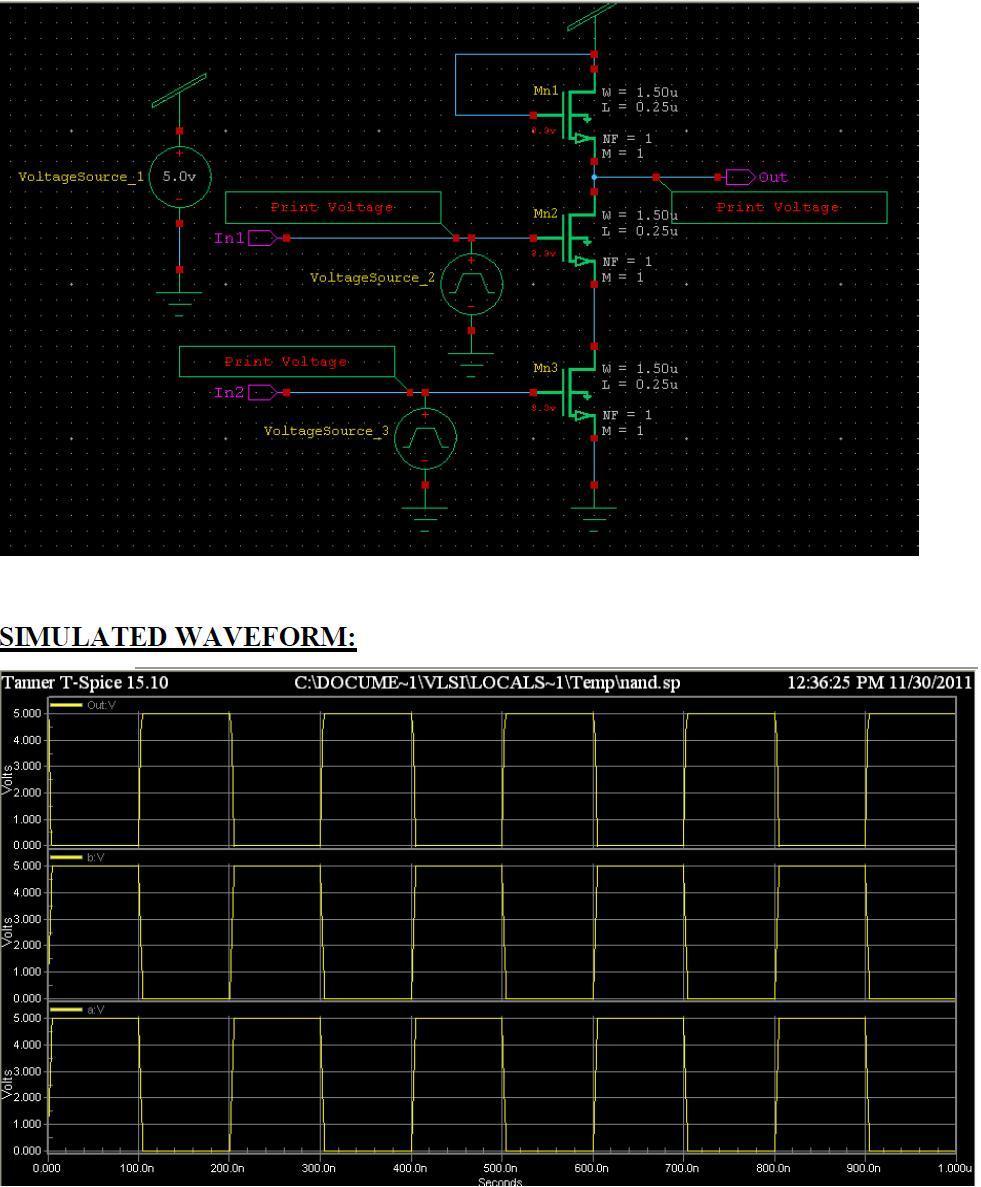
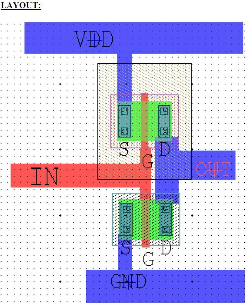
37 Automatic Layout Generation Ex No: Date: OBJECTIVE OF THE EXPERIMENT To generate the Layout from the schematic using the Tanner tool and verify the layout using simulation. FACILITIES REQUIRED AND PROCEDURE a) Facilities required to do the experiment S.No. SOFTWARE REQUIREMENTS Quantity 1 S-Edit, L-Edit using Tanner Tool 1 b) Procedure for doing the experiment S.No Details of the step 1 Draw the schematic using S Edit and verify the output in W Edit. 2 Extract the schematic and store it in another location 3 Open the L Edit, open the design in Ring VCO 4 Create the new cell 5 Open the schematic file (.sdl) using the SDL Navigator 6 Do the necessary connections as per the design. 7 Name the ports and check the design for the DRC Rules 8 Locate the Destination file in the setup Extract window and extract the layout. 9 Include the Library and the print voltage statements in the net list which is obtained. 10 Verify the layout design using W Edit.

38 SCHEMATIC DIAGRAM
39

40 RESULT Thus the the Layout from the schematic using the Cadance tool and verify the layout using simulation and the output also verified successfully.
41 Implementation Of Flip-Flops Ex No: Date: OBJECTIVE OF THE EXPERIMENT To implement Flip-flops using Verilog HDL. FACILITIES REQUIRED AND PROCEDURE a) Facilities required to do the experiment S.No. SOFTWARE REQUIREMENTS Quantity 1 Xilinx Project navigator ISE b) Procedure for doing the experiment S.No Details of the step 1 Double click the project navigator and select the option File-New project. 2 Give the project name. 3 Select Verilog module. 4 Type your verilog coding. 5 Check for syntax. 6 Select the new source of test bench waveform 7 Choose behavioral simulation and simulate it by Xilinx ISE simulator. 8 Verify the output.
42 D Flip-Flop // Module Name: DFF module DFF(Clock, Reset, d, q); input Clock; input Reset; input d; output q; reg q; Clock or negedge Reset) if (~Reset) q=1'b0; else q=d; endmodule T Flip-Flop // Module Name: TFF module TFF(Clock, Reset, t, q); input Clock; input Reset; input t; output q; reg q; always@(posedge Clock, negedge Reset) if(~reset) q=0; else if (t) q=~q; else q=q; endmodule
43 JK Flip-Flop // Module Name: JKFF module JKFF(Clock, Reset, j, k, q); input Clock; input Reset; input j; input k; output q; reg q; Clock, negedge Reset) if(~reset) q=0; else begin case({j,k}) 2'b00: q=q; 2'b01: q=0; 2'b10: q=1; 2'b11: q=~q; endcase end endmodule RESULT Thus the flip-flops program was implemented using tools and the output also verified successfully.
44 Implementation Of Counters Ex No: Date: OBJECTIVE OF THE EXPERIMENT To implement Counters using Verilog HDL. FACILITIES REQUIRED AND PROCEDURE a) Facilities required to do the experiment S.No. SOFTWARE REQUIREMENTS Quantity 1 Xilinx Project navigator ISE b) Procedure for doing the experiment S.No Details of the step 1 Double click the project navigator and select the option File-New project. 2 Give the project name. 3 Select Verilog module. 4 Type your verilog coding. 5 Check for syntax. 6 Select the new source of test bench waveform 7 Choose behavioral simulation and simulate it by xilinx ISE simulator. 8 Verify the output.
45 DEPT OF ECE 2- Bit Counter // Module Name: Count2Bit module Count2Bit(Clock, Clear, out); input Clock; input Clear; output [1:0] out; reg [1:0]out; Clock, negedge Clear) if((~clear) (out>=4)) out=2'b00; else out=out+1; endmodule RESULT Thus the counters program was implemented using tools and the output also verified successfully.
46 DEPT OF ECE Implementation Of Registers Ex No: Date: OBJECTIVE OF THE EXPERIMENT To implement Registers using Verilog HDL. FACILITIES REQUIRED AND PROCEDURE a) Facilities required to do the experiment S.No. SOFTWARE REQUIREMENTS Quantity 1 Xilinx Project navigator ISE b) Procedure for doing the experiment S.No Details of the step 1 Double click the project navigator and select the option File-New project. 2 Give the project name. 3 Select Verilog module. 4 Type your Verilog coding. 5 Check for syntax. 6 Select the new source of test bench waveform 7 Choose behavioral simulation and simulate it by Xilinx ISE simulator. 8 Verify the output.
47 DEPT OF ECE 2 Bit Register // Module Name: Reg2Bit module Reg2Bit(Clock, Clear, in, out); input Clock; input Clear; input [0:1] in; output [0:1] out; reg [0:1] out; always@(posedge Clock, negedge Clear) if(~clear) out=2'b00; else out=in; endmodule RESULT Thus the Registers program was implemented using tools and the output also verified successfully.
Dr NNCE ECE/VI-SEM VLSI DESIGN LAB-LM
 EC2357-VLSI DESIGN LABORATORY LABORATORY MANUAL FOR SIXTH SEMESTER B.E (ECE) (FOR PRIVATE CIRCULATION ONLY) ACADEMIC YEAR(2013-2014) ANNA UNIVERSITY, CHENNAI-25 DEPARTMENT OF ELECTRONICS AND COMMUNICATION
 PAGE NO: EXP NO: 1A SIMULATION OF HALF ADDER AND FULL ADDER. DATE: AIM: To design, simulate and synthesize the Half adder and Full adder. TOOLS REQUIRED: SOFTWARE: XILINX ISE 9.1i ALGORITHM: 1. Start the
Department of Computer Science & Engineering. Lab Manual DIGITAL LAB. Class: 2nd yr, 3rd sem SYLLABUS
 Department of Computer Science & Engineering Lab Manual 435 DIGITAL LAB Class: 2nd yr, 3rd sem SYLLABUS. Verification of Boolean theorems using digital logic gates. 2. Design and implementation of code
N-input EX-NOR gate. N-output inverter. N-input NOR gate
 Hardware Description Language HDL Introduction HDL is a hardware description language used to design and document electronic systems. HDL allows designers to design at various levels of abstraction. It
PINE TRAINING ACADEMY
 PINE TRAINING ACADEMY Course Module A d d r e s s D - 5 5 7, G o v i n d p u r a m, G h a z i a b a d, U. P., 2 0 1 0 1 3, I n d i a Digital Logic System Design using Gates/Verilog or VHDL and Implementation
Digital Design with FPGAs. By Neeraj Kulkarni
 Digital Design with FPGAs By Neeraj Kulkarni Some Basic Electronics Basic Elements: Gates: And, Or, Nor, Nand, Xor.. Memory elements: Flip Flops, Registers.. Techniques to design a circuit using basic
FPGA Design Challenge :Techkriti 14 Digital Design using Verilog Part 1
 FPGA Design Challenge :Techkriti 14 Digital Design using Verilog Part 1 Anurag Dwivedi Digital Design : Bottom Up Approach Basic Block - Gates Digital Design : Bottom Up Approach Gates -> Flip Flops Digital
Federal Urdu University of Arts, Science and Technology, Islamabad VLSI SYSTEM DESIGN. Prepared By: Engr. Yousaf Hameed.
 VLSI SYSTEM DESIGN Prepared By: Engr. Yousaf Hameed Lab Engineer BASIC ELECTRICAL & DIGITAL SYSTEMS LAB DEPARTMENT OF ELECTRICAL ENGINEERING VLSI System Design 1 LAB 01 Schematic Introduction to DSCH and
Circuit Design and Simulation with VHDL 2nd edition Volnei A. Pedroni MIT Press, 2010 Book web:
 Circuit Design and Simulation with VHDL 2nd edition Volnei A. Pedroni MIT Press, 2010 Book web: www.vhdl.us Appendix C Xilinx ISE Tutorial (ISE 11.1) This tutorial is based on ISE 11.1 WebPack (free at
DIGITAL SYSTEM DESIGN
 DIGITAL SYSTEM DESIGN Prepared By: Engr. Yousaf Hameed Lab Engineer BASIC ELECTRICAL & DIGITAL SYSTEMS LAB DEPARTMENT OF ELECTRICAL ENGINEERING Digital System Design 1 Name: Registration No: Roll No: Semester:
ICAL ENG LAB MANUAL EC6612- VLSI DESIGN LABORATORY. Dharmapuri : B.E. ECE. Branch EC6612 VLSI DESIGN LAB
 1 Dharmapuri 636 703 LAB MANUAL Regulation : 2013 Branch : B.E. ECE Year & Semester : III Year / VI Semester EC6612- VLSI DESIGN LABORATORY ICAL ENG 2 ANNA UNIVERSITY CHENNAI Regulation 2013 FPGA BASED
A STUDY OF DESIGN TOOL - XILINX
 A STUDY OF DESIGN TOOL - XILINX 1. Open Xilinx Project Navigator from Start Menu Xilinx ISE Opens-up 2. Opening a New ProjectSelect New Project from File Menu The below window opensup Enter the Project
Lab 6 : Introduction to Verilog
 Lab 6 : Introduction to Verilog Name: Sign the following statement: On my honor, as an Aggie, I have neither given nor received unauthorized aid on this academic work 1 Objective The main objective of
CMOS Design Lab Manual
 CMOS Design Lab Manual Developed By University Program Team CoreEl Technologies (I) Pvt. Ltd. 1 Objective Objective of this lab is to learn the Mentor Graphics HEP2 tools as well learn the flow of the
ESE 570 Cadence Lab Assignment 2: Introduction to Spectre, Manual Layout Drawing and Post Layout Simulation (PLS)
") ESE 570 Cadence Lab Assignment 2: Introduction to Spectre, Manual Layout Drawing and Post Layout Simulation (PLS) Objective Part A: To become acquainted with Spectre (or HSpice) by simulating an inverter,
ESE 570 Cadence Lab Assignment 2: Introduction to Spectre, Manual Layout Drawing and Post Layout Simulation (PLS) Objective Part A: To become acquainted with Spectre (or HSpice) by simulating an inverter,
Verilog Fundamentals. Shubham Singh. Junior Undergrad. Electrical Engineering
 Verilog Fundamentals Shubham Singh Junior Undergrad. Electrical Engineering VERILOG FUNDAMENTALS HDLs HISTORY HOW FPGA & VERILOG ARE RELATED CODING IN VERILOG HDLs HISTORY HDL HARDWARE DESCRIPTION LANGUAGE
UNIT V: SPECIFICATION USING VERILOG HDL
 UNIT V: SPECIFICATION USING VERILOG HDL PART -A (2 Marks) 1. What are identifiers? Identifiers are names of modules, variables and other objects that we can reference in the design. Identifiers consists
CSE 591: Advanced Hardware Design and Verification (2012 Spring) LAB #0
 LAB #0") Lab 0: Tutorial on Xilinx Project Navigator & ALDEC s Active-HDL Simulator CSE 591: Advanced Hardware Design and Verification Assigned: 01/05/2011 Due: 01/19/2011 Table of Contents 1 Overview... 2 1.1
Lab 0: Tutorial on Xilinx Project Navigator & ALDEC s Active-HDL Simulator CSE 591: Advanced Hardware Design and Verification Assigned: 01/05/2011 Due: 01/19/2011 Table of Contents 1 Overview... 2 1.1
Actel Libero TM Integrated Design Environment v2.3 Structural Schematic Flow Design Tutorial
 Actel Libero TM Integrated Design Environment v2.3 Structural Schematic Flow Design Tutorial 1 Table of Contents Design Flow in Libero TM IDE v2.3 Step 1 - Design Creation 3 Step 2 - Design Verification
ENGN 1630: CPLD Simulation Fall ENGN 1630 Fall Simulating XC9572XLs on the ENGN1630 CPLD-II Board Using Xilinx ISim
 ENGN 1630 Fall 2018 Simulating XC9572XLs on the ENGN1630 CPLD-II Board Using Xilinx ISim You will use the Xilinx ISim simulation software for the required timing simulation of the XC9572XL CPLD programmable
FACULTY OF ENGINEERING MULTIMEDIA UNIVERSITY LAB SHEET DIGITAL INTEGRATED CIRCUIT
 FACULTY OF ENGINEERING MULTIMEDIA UNIVERSITY LAB SHEET DIGITAL INTEGRATED CIRCUIT DIC1: Schematic Design Entry, Simulation & Verification DIC2: Schematic Driven Layout Drawing (SDL) Design Rule Check (DRC)
After opening the Programs> Xilinx ISE 8.2i > Project Navigator, you will come to this screen as start-up.
 After opening the Programs> Xilinx ISE 8.2i > Project Navigator, you will come to this screen as start-up. Start with a new project. Enter a project name and be sure to select Schematic as the Top-Level
Digital Circuit Design and Language. Datapath Design. Chang, Ik Joon Kyunghee University
 Digital Circuit Design and Language Datapath Design Chang, Ik Joon Kyunghee University Typical Synchronous Design + Control Section : Finite State Machine + Data Section: Adder, Multiplier, Shift Register
Verilog Tutorial (Structure, Test)
") Digital Circuit Design and Language Verilog Tutorial (Structure, Test) Chang, Ik Joon Kyunghee University Hierarchical Design Top-down Design Methodology Bottom-up Design Methodology Module START Example)
Digital Circuit Design and Language Verilog Tutorial (Structure, Test) Chang, Ik Joon Kyunghee University Hierarchical Design Top-down Design Methodology Bottom-up Design Methodology Module START Example)
ENEE245 Digital Circuits and Systems Lab Manual
 ENEE245 Digital Circuits and Systems Lab Manual Department of Engineering, Physical & Computer Sciences Montgomery College Version 1.1 Copyright Prof. Lan Xiang (Do not distribute without permission) 1
Logic Circuits II ECE 2411 Thursday 4:45pm-7:20pm. Lecture 3
 Logic Circuits II ECE 2411 Thursday 4:45pm-7:20pm Lecture 3 Lecture 3 Topics Covered: Chapter 4 Discuss Sequential logic Verilog Coding Introduce Sequential coding Further review of Combinational Verilog
Chennai Institute of Technology Sarathy Nagar, Pudupedu, Kundrathur, Chennai Department of Electronics and Communication Engineering
 Ex. No. 6 Date: CARRY SELECT ADDER Aim: To simulate and synthesis Carry Select Adder using Verilog HDL Software tools Required: Theory: Synthesis tool: Xilinx ISE. Simulation tool: Project navigator Simulator
LABORATORY MANUAL VLSI DESIGN LAB EE-330-F
 LABORATORY MANUAL VLSI DESIGN LAB EE-330-F (VI th Semester) Prepared By: Vikrant Verma B. Tech. (ECE), M. Tech. (ECE) Department of Electrical & Electronics Engineering BRCM College of Engineering & Technology
ENEE245 Digital Circuits and Systems Lab Manual
 ENEE245 Digital Circuits and Systems Lab Manual Department of Engineering, Physical & Computer Sciences Montgomery College Modified Fall 2017 Copyright Prof. Lan Xiang (Do not distribute without permission)
Spiral 2-8. Cell Layout
 2-8.1 Spiral 2-8 Cell Layout 2-8.2 Learning Outcomes I understand how a digital circuit is composed of layers of materials forming transistors and wires I understand how each layer is expressed as geometric
Verilog Design Entry, Synthesis, and Behavioral Simulation
 ------------------------------------------------------------- PURPOSE - This lab will present a brief overview of a typical design flow and then will start to walk you through some typical tasks and familiarize
: : (91-44) (Office) (91-44) (Residence)
 (Office) (91-44) (Residence)") Course: VLSI Circuits (Video Course) Faculty Coordinator(s) : Prof. S. Srinivasan Department of Electrical Engineering Indian Institute of Technology Madras Chennai 600036 Email Telephone : srinis@iitm.ac.in,
Course: VLSI Circuits (Video Course) Faculty Coordinator(s) : Prof. S. Srinivasan Department of Electrical Engineering Indian Institute of Technology Madras Chennai 600036 Email Telephone : srinis@iitm.ac.in,
Lab 7 (Sections 300, 301 and 302) Prelab: Introduction to Verilog
 Prelab: Introduction to Verilog") Lab 7 (Sections 300, 301 and 302) Prelab: Introduction to Verilog Name: Sign the following statement: On my honor, as an Aggie, I have neither given nor received unauthorized aid on this academic work
Lab 7 (Sections 300, 301 and 302) Prelab: Introduction to Verilog Name: Sign the following statement: On my honor, as an Aggie, I have neither given nor received unauthorized aid on this academic work
Cadence Tutorial A: Schematic Entry and Functional Simulation Created for the MSU VLSI program by Andrew Mason and the AMSaC lab group.
 Cadence Tutorial A: Schematic Entry and Functional Simulation Created for the MSU VLSI program by Andrew Mason and the AMSaC lab group. Revision Notes: Aug. 2003 update and edit A. Mason add intro/revision/contents
Xilinx Tutorial Basic Walk-through
 Introduction to Digital Logic Design with FPGA s: Digital logic circuits form the basis of all digital electronic devices. FPGAs (Field Programmable Gate Array) are large programmable digital electronic
ECE 4514 Digital Design II. Spring Lecture 2: Hierarchical Design
 ECE 4514 Digital Design II Spring 2007 Abstraction in Hardware Design Remember from last lecture that HDLs offer a textual description of a netlist. Through abstraction in the HDL, we can capture more
TUTORIAL II ECE 555 / 755 Updated on September 11 th 2006 CADENCE LAYOUT AND PARASITIC EXTRACTION
 TUTORIAL II ECE 555 / 755 Updated on September 11 th 2006 CADENCE LAYOUT AND PARASITIC EXTRACTION After finishing a schematic of your design (Tutorial-I), the next step is creating masks which are for
Brief Introduction of Cell-based Design. Ching-Da Chan CIC/DSD
 Brief Introduction of Cell-based Design Ching-Da Chan CIC/DSD 1 Design Abstraction Levels SYSTEM MODULE + GATE CIRCUIT S n+ G DEVICE n+ D 2 Full Custom V.S Cell based Design Full custom design Better patent
Graduate Institute of Electronics Engineering, NTU. FPGA Lab. Speaker : 鍾明翰 (CMH) Advisor: Prof. An-Yeu Wu Date: 2010/12/14 ACCESS IC LAB
 Advisor: Prof. An-Yeu Wu Date: 2010/12/14 ACCESS IC LAB") FPGA Lab Speaker : 鍾明翰 (CMH) Advisor: Prof. An-Yeu Wu Date: 2010/12/14 ACCESS IC LAB Objective In this Lab, you will learn the basic set-up and design methods of implementing your design by ISE 10.1. Create
FPGA Lab Speaker : 鍾明翰 (CMH) Advisor: Prof. An-Yeu Wu Date: 2010/12/14 ACCESS IC LAB Objective In this Lab, you will learn the basic set-up and design methods of implementing your design by ISE 10.1. Create
and 32 bit for 32 bit. If you don t pay attention to this, there will be unexpected behavior in the ISE software and thing may not work properly!
 This tutorial will show you how to: Part I: Set up a new project in ISE 14.7 Part II: Implement a function using Schematics Part III: Simulate the schematic circuit using ISim Part IV: Constraint, Synthesize,
101-1 Under-Graduate Project Digital IC Design Flow
 101-1 Under-Graduate Project Digital IC Design Flow Speaker: Ming-Chun Hsiao Adviser: Prof. An-Yeu Wu Date: 2012/9/25 ACCESS IC LAB Outline Introduction to Integrated Circuit IC Design Flow Verilog HDL
DESIGN STRATEGIES & TOOLS UTILIZED
 CHAPTER 7 DESIGN STRATEGIES & TOOLS UTILIZED 7-1. Field Programmable Gate Array The internal architecture of an FPGA consist of several uncommitted logic blocks in which the design is to be encoded. The
INSTITUTE OF AERONAUTICAL ENGINEERING Dundigal, Hyderabad ELECTRONICS AND COMMUNICATIONS ENGINEERING
 INSTITUTE OF AERONAUTICAL ENGINEERING Dundigal, Hyderabad - 00 0 ELECTRONICS AND COMMUNICATIONS ENGINEERING QUESTION BANK Course Name : DIGITAL DESIGN USING VERILOG HDL Course Code : A00 Class : II - B.
TLL5000 Electronic System Design Base Module. Getting Started Guide, Ver 3.4
 TLL5000 Electronic System Design Base Module Getting Started Guide, Ver 3.4 COPYRIGHT NOTICE The Learning Labs, Inc. ( TLL ) All rights reserved, 2008 Reproduction in any form without permission is prohibited.
St.MARTIN S ENGINEERING COLLEGE Dhulapally, Secunderabad
 St.MARTIN S ENGINEERING COLLEGE Dhulapally, Secunderabad-500 014 Subject: Digital Design Using Verilog Hdl Class : ECE-II Group A (Short Answer Questions) UNIT-I 1 Define verilog HDL? 2 List levels of
Graphics: Alexandra Nolte, Gesine Marwedel, Universität Dortmund. RTL Synthesis
 Graphics: Alexandra Nolte, Gesine Marwedel, 2003 Universität Dortmund RTL Synthesis Purpose of HDLs Purpose of Hardware Description Languages: Capture design in Register Transfer Language form i.e. All
FPGA Design Flow 1. All About FPGA
 FPGA Design Flow 1 In this part of tutorial we are going to have a short intro on FPGA design flow. A simplified version of FPGA design flow is given in the flowing diagram. FPGA Design Flow 2 FPGA_Design_FLOW
2IN35 VLSI Programming Lab Work Assignment 1: Hardware design using Verilog
 2IN35 VLSI Programming Lab Work Assignment 1: Hardware design using Verilog Hrishikesh Salunkhe, h.l.salunkhe@tue.nl, Alok Lele, a.lele@tue.nl April 28, 2015 1 Contents 1 Introduction 3 2 Hardware design
Design rule illustrations for the AMI C5N process can be found at:
 Cadence Tutorial B: Layout, DRC, Extraction, and LVS Created for the MSU VLSI program by Professor A. Mason and the AMSaC lab group. Revised by C Young & Waqar A Qureshi -FS08 Document Contents Introduction
Lab. Course Goals. Topics. What is VLSI design? What is an integrated circuit? VLSI Design Cycle. VLSI Design Automation
 Course Goals Lab Understand key components in VLSI designs Become familiar with design tools (Cadence) Understand design flows Understand behavioral, structural, and physical specifications Be able to
University of Hawaii EE 361L. Getting Started with Spartan 3E Digilent Basys2 Board. Lab 4.1
 University of Hawaii EE 361L Getting Started with Spartan 3E Digilent Basys2 Board Lab 4.1 I. Test Basys2 Board Attach the Basys2 board to the PC or laptop with the USB connector. Make sure the blue jumper
MLR Institute of Technology
 MLR Institute of Technology Laxma Reddy Avenue, Dundigal, Quthbullapur (M), Hyderabad 500 043 Course Name Course Code Class Branch ELECTRONICS AND COMMUNICATIONS ENGINEERING QUESTION BANK : DIGITAL DESIGN
Tutorial: Working with the Xilinx tools 14.4
 Tutorial: Working with the Xilinx tools 14.4 This tutorial will show you how to: Part I: Set up a new project in ISE Part II: Implement a function using Schematics Part III: Implement a function using
Graduate Institute of Electronics Engineering, NTU FPGA Design with Xilinx ISE
 FPGA Design with Xilinx ISE Presenter: Shu-yen Lin Advisor: Prof. An-Yeu Wu 2005/6/6 ACCESS IC LAB Outline Concepts of Xilinx FPGA Xilinx FPGA Architecture Introduction to ISE Code Generator Constraints
EECS 150 Homework 7 Solutions Fall (a) 4.3 The functions for the 7 segment display decoder given in Section 4.3 are:
 4.3 The functions for the 7 segment display decoder given in Section 4.3 are:") Problem 1: CLD2 Problems. (a) 4.3 The functions for the 7 segment display decoder given in Section 4.3 are: C 0 = A + BD + C + BD C 1 = A + CD + CD + B C 2 = A + B + C + D C 3 = BD + CD + BCD + BC C 4
Problem 1: CLD2 Problems. (a) 4.3 The functions for the 7 segment display decoder given in Section 4.3 are: C 0 = A + BD + C + BD C 1 = A + CD + CD + B C 2 = A + B + C + D C 3 = BD + CD + BCD + BC C 4
ECE 4514 Digital Design II. Spring Lecture 20: Timing Analysis and Timed Simulation
 ECE 4514 Digital Design II Lecture 20: Timing Analysis and Timed Simulation A Tools/Methods Lecture Topics Static and Dynamic Timing Analysis Static Timing Analysis Delay Model Path Delay False Paths Timing
CPLD Experiment 4. XOR and XNOR Gates with Applications
 CPLD Experiment 4 XOR and XNOR Gates with Applications Based on Xilinx ISE Design Suit 10.1 Department of Electrical & Computer Engineering Florida International University Objectives Materials Examining
Lab 1: Introduction to Verilog HDL and the Xilinx ISE
 EE 231-1 - Fall 2016 Lab 1: Introduction to Verilog HDL and the Xilinx ISE Introduction In this lab simple circuits will be designed by programming the field-programmable gate array (FPGA). At the end
Revision: February 27, E Main Suite D Pullman, WA (509) Voice and Fax
 Voice and Fax") Xilinx ISE WebPACK Schematic Capture Tutorial Revision: February 27, 2010 215 E Main Suite D Pullman, WA 99163 (509) 334 6306 Voice and Fax Overview This tutorial provides instruction for using the Xilinx
Xilinx ISE WebPACK Schematic Capture Tutorial Revision: February 27, 2010 215 E Main Suite D Pullman, WA 99163 (509) 334 6306 Voice and Fax Overview This tutorial provides instruction for using the Xilinx
Xilinx Schematic Entry Tutorial
 Overview Xilinx Schematic Entry Tutorial Xilinx ISE Schematic Entry & Modelsim Simulation What is circuit simulation and why is it important? Complex designs, short design cycle Simultaneous system design
FPGA for Complex System Implementation. National Chiao Tung University Chun-Jen Tsai 04/14/2011
 FPGA for Complex System Implementation National Chiao Tung University Chun-Jen Tsai 04/14/2011 About FPGA FPGA was invented by Ross Freeman in 1989 SRAM-based FPGA properties Standard parts Allowing multi-level
Why Should I Learn This Language? VLSI HDL. Verilog-2
 Verilog Why Should I Learn This Language? VLSI HDL Verilog-2 Different Levels of Abstraction Algorithmic the function of the system RTL the data flow the control signals the storage element and clock Gate
Lecture 1: Introduction Course arrangements Recap of basic digital design concepts EDA tool demonstration
 TKT-1426 Digital design for FPGA, 6cp Fall 2011 http://www.tkt.cs.tut.fi/kurssit/1426/ Tampere University of Technology Department of Computer Systems Waqar Hussain Lecture Contents Lecture 1: Introduction
Programmable Logic Design I
 Programmable Logic Design I Introduction In labs 11 and 12 you built simple logic circuits on breadboards using TTL logic circuits on 7400 series chips. This process is simple and easy for small circuits.
Sequential Logic Blocks
 Sequential Logic Blocks Output of sequential blocks depends on present state as well as on past state. Sequential circuits work with a reference which is clock. A clock signal can be of any duty cycle,
EE 330 Spring Laboratory 2: Basic Boolean Circuits
 EE 330 Spring 2013 Laboratory 2: Basic Boolean Circuits Objective: The objective of this experiment is to investigate methods for evaluating the performance of Boolean circuits. Emphasis will be placed
S Exercise 1C Testing the Ring Oscillator
 S-87.3148 Exercise 1C Testing the Ring Oscillator Aalto University School of Electrical Engineering Department of Micro- and Nanosciences (ECDL) 10.9.2014 1 1 Building the test bench In this exercise,
EE 1315 DIGITAL LOGIC LAB EE Dept, UMD
 EE 1315 DIGITAL LOGIC LAB EE Dept, UMD EXPERIMENT # 1: Logic building blocks The main objective of this experiment is to let you familiarize with the lab equipment and learn about the operation of the
Laboratory 6. - Using Encounter for Automatic Place and Route. By Mulong Li, 2013
 CME 342 (VLSI Circuit Design) Laboratory 6 - Using Encounter for Automatic Place and Route By Mulong Li, 2013 Reference: Digital VLSI Chip Design with Cadence and Synopsys CAD Tools, Erik Brunvand Background
EE 1315: DIGITAL LOGIC LAB EE Dept, UMD
 EXPERIMENT # 7: Basic Latches EE 1315: DIGITAL LOGIC LAB EE Dept, UMD Latches are primitive memory elements of sequential circuits that are used in building simple noise filtering circuits and flip-flops.
Laboratory of Digital Circuits Design: Design, Implementation and Simulation of Digital Circuits Using Programmable Devices
 Internet Engineering Dr. Jarosław Sugier Laboratory of Digital Circuits Design: Design, Implementation and Simulation of Digital Circuits Using Programmable Devices This document presents software packages
An overview of standard cell based digital VLSI design
 An overview of standard cell based digital VLSI design Implementation of the first generation AsAP processor Zhiyi Yu and Tinoosh Mohsenin VCL Laboratory UC Davis Outline Overview of standard cellbased
An easy to read reference is:
 1. Synopsis: Timing Analysis and Timing Constraints The objective of this lab is to make you familiar with two critical reports produced by the Xilinx ISE during your design synthesis and implementation.
Step 1: Downloading the source files
 Introduction: In this lab and in the remainder of the ELEC 2607 labs, you will be using the Xilinx ISE to enter and simulate the designs for your circuits. In labs 3 and 4, you will use ISE to compile
6. Latches and Memories
 6 Latches and Memories This chapter . RS Latch The RS Latch, also called Set-Reset Flip Flop (SR FF), transforms a pulse into a continuous state. The RS latch can be made up of two interconnected
ELEC 204 Digital System Design LABORATORY MANUAL
 ELEC 204 Digital System Design LABORATORY MANUAL : Introductory Tutorial For Xilinx ISE Foundation v10.1 & Implementing XOR Gate College of Engineering Koç University Important Note: In order to effectively
Synthesis of Combinational and Sequential Circuits with Verilog
 Synthesis of Combinational and Sequential Circuits with Verilog What is Verilog? Hardware description language: Are used to describe digital system in text form Used for modeling, simulation, design Two
ECE 2300 Digital Logic & Computer Organization. More Sequential Logic Verilog
 ECE 2300 Digital Logic & Computer Organization Spring 2018 More Sequential Logic Verilog Lecture 7: 1 Announcements HW3 will be posted tonight Prelim 1 Thursday March 1, in class Coverage: Lectures 1~7
ENEE 245 Lab 1 Report Rubrics
 ENEE 4 Lab 1 Report Rubrics Design Clearly state the design requirements Derive the minimum SOP Show the circuit implementation. Draw logic diagram and wiring diagram neatly Label all the diagrams/tables
TLL5000 Electronic System Design Base Module
 TLL5000 Electronic System Design Base Module The Learning Labs, Inc. Copyright 2007 Manual Revision 2007.12.28 1 Copyright 2007 The Learning Labs, Inc. Copyright Notice The Learning Labs, Inc. ( TLL )
(ii) Simplify and implement the following SOP function using NOR gates:
 Simplify and implement the following SOP function using NOR gates:") DHANALAKSHMI COLLEGE OF ENGINEERING DEPARTMENT OF ELECTRONICS AND COMMUNICATION ENGINEERING EE6301 DIGITAL LOGIC CIRCUITS UNIT I NUMBER SYSTEMS AND DIGITAL LOGIC FAMILIES PART A 1. How can an OR gate be
DHANALAKSHMI COLLEGE OF ENGINEERING DEPARTMENT OF ELECTRONICS AND COMMUNICATION ENGINEERING EE6301 DIGITAL LOGIC CIRCUITS UNIT I NUMBER SYSTEMS AND DIGITAL LOGIC FAMILIES PART A 1. How can an OR gate be
ANADOLU UNIVERSITY DEPARTMENT OF ELECTRICAL AND ELECTRONICS ENGINEERING. EEM Digital Systems II
 ANADOLU UNIVERSITY DEPARTMENT OF ELECTRICAL AND ELECTRONICS ENGINEERING EEM 334 - Digital Systems II LAB 1 - INTRODUCTION TO XILINX ISE SOFTWARE AND FPGA 1. PURPOSE In this lab, after you learn to use
Lab 2. Standard Cell layout.
 Lab 2. Standard Cell layout. The purpose of this lab is to demonstrate CMOS-standard cell design. Use the lab instructions and the cadence manual (http://www.es.lth.se/ugradcourses/cadsys/cadence.html)
Introduction to CMOS VLSI Design (E158) Lab 4: Controller Design
 Lab 4: Controller Design") Harris Introduction to CMOS VLSI Design (E158) Lab 4: Controller Design The controller for your MIPS processor is responsible for generating the signals to the datapath to fetch and execute each instruction.
Harris Introduction to CMOS VLSI Design (E158) Lab 4: Controller Design The controller for your MIPS processor is responsible for generating the signals to the datapath to fetch and execute each instruction.
FPGA Design Tutorial
 ECE 554 Digital Engineering Laboratory FPGA Design Tutorial Version 5.0 Fall 2006 Updated Tutorial: Jake Adriaens Original Tutorial: Matt King, Surin Kittitornkun and Charles R. Kime Table of Contents
Cadence Tutorial A: Schematic Entry and Functional Simulation Created for the MSU VLSI program by Professor A. Mason and the AMSaC lab group.
 Cadence Tutorial A: Schematic Entry and Functional Simulation Created for the MSU VLSI program by Professor A. Mason and the AMSaC lab group. Revision Notes: Jan. 2006 Updated for use with spectre simulator
Xilinx ASMBL Architecture
 FPGA Structure Xilinx ASMBL Architecture Design Flow Synthesis: HDL to FPGA primitives Translate: FPGA Primitives to FPGA Slice components Map: Packing of Slice components into Slices, placement of Slices
Speaker: Shao-Wei Feng Adviser: Prof. An-Yeu Wu Date: 2010/09/28
 99-1 Under-Graduate Project Verilog Simulation & Debugging Tools Speaker: Shao-Wei Feng Adviser: Prof. An-Yeu Wu Date: 2010/09/28 ACCESS IC LAB Outline Basic Concept of Verilog HDL Gate Level Modeling
Introduction to Verilog HDL. Verilog 1
 Introduction to HDL Hardware Description Language (HDL) High-Level Programming Language Special constructs to model microelectronic circuits Describe the operation of a circuit at various levels of abstraction
Virtuoso Layout Editor
 This tutorial will cover the basic steps involved in using the Cadence layout editor called Virtuoso, extracting layout, and running simulation on the layout. The inverter layout is used as an example
Digital Logic Design Lab
 Digital Logic Design Lab DEPARTMENT OF ELECTRICAL ENGINEERING LAB BROCHURE DIGITAL LOGIC DESIGN LABORATORY CONTENTS Lab Venue... 3 Lab Objectives & Courses... 3 Lab Description & Experiments... 4 Hardware
EE 330 Laboratory Experiment Number 11
 EE 330 Laboratory Experiment Number 11 Design and Simulation of Digital Circuits using Hardware Description Languages Fall 2017 Contents Purpose:... 3 Background... 3 Part 1: Inverter... 4 1.1 Simulating
EECS150, Fall 2004, Midterm 1, Prof. Culler. Problem 1 (15 points) 1.a. Circle the gate-level circuits that DO NOT implement a Boolean AND function.
 1.a. Circle the gate-level circuits that DO NOT implement a Boolean AND function.") Problem 1 (15 points) 1.a. Circle the gate-level circuits that DO NOT implement a Boolean AND function. 1.b. Show that a 2-to-1 MUX is universal (i.e. that any Boolean expression can be implemented with
Problem 1 (15 points) 1.a. Circle the gate-level circuits that DO NOT implement a Boolean AND function. 1.b. Show that a 2-to-1 MUX is universal (i.e. that any Boolean expression can be implemented with
Institute of Engineering & Management
 Course:CS493- Computer Architecture Lab PROGRAMME: COMPUTERSCIENCE&ENGINEERING DEGREE:B. TECH COURSE: Computer Architecture Lab SEMESTER: 4 CREDITS: 2 COURSECODE: CS493 COURSE TYPE: Practical COURSE AREA/DOMAIN:
Introduction to Verilog/System Verilog
 NTUEE DCLAB Feb. 27, 2018 Introduction to Verilog/System Verilog Presenter: Yao-Pin Wang 王耀斌 Advisor: Prof. Chia-Hsiang Yang 楊家驤 Dept. of Electrical Engineering, NTU National Taiwan University What is
Modeling Synchronous Logic Circuits. Debdeep Mukhopadhyay IIT Madras
 Modeling Synchronous Logic Circuits Debdeep Mukhopadhyay IIT Madras Basic Sequential Circuits A combinational circuit produces output solely depending on the current input. But a sequential circuit remembers
INTRODUCTION TO CATAPULT C
 INTRODUCTION TO CATAPULT C Vijay Madisetti, Mohanned Sinnokrot Georgia Institute of Technology School of Electrical and Computer Engineering with adaptations and updates by: Dongwook Lee, Andreas Gerstlauer
CSCB58 - Lab 3. Prelab /3 Part I (in-lab) /2 Part II (in-lab) /2 TOTAL /8
 /2 Part II (in-lab) /2 TOTAL /8") CSCB58 - Lab 3 Latches, Flip-flops, and Registers Learning Objectives The purpose of this exercise is to investigate the fundamental synchronous logic elements: latches, flip-flops, and registers. Prelab
CSCB58 - Lab 3 Latches, Flip-flops, and Registers Learning Objectives The purpose of this exercise is to investigate the fundamental synchronous logic elements: latches, flip-flops, and registers. Prelab
CPE/EE 427, CPE 527, VLSI Design I: Tutorial #2, Schematic Capture, DC Analysis, Transient Analysis (Inverter, NAND2)
") CPE/EE 427, CPE 527, VLSI Design I: Tutorial #2, Schematic Capture, DC Analysis, Transient Analysis (Inverter, NAND2) Joel Wilder, Aleksandar Milenkovic, ECE Dept., The University of Alabama in Huntsville
CPE/EE 427, CPE 527, VLSI Design I: Tutorial #2, Schematic Capture, DC Analysis, Transient Analysis (Inverter, NAND2) Joel Wilder, Aleksandar Milenkovic, ECE Dept., The University of Alabama in Huntsville
Using ModelSim to Simulate Logic Circuits for Altera FPGA Devices
 Using ModelSim to Simulate Logic Circuits for Altera FPGA Devices This tutorial is a basic introduction to ModelSim, a Mentor Graphics simulation tool for logic circuits. We show how to perform functional