Dr NNCE ECE/VI-SEM VLSI DESIGN LAB-LM
|
|
|
- Corey Harmon
- 6 years ago
- Views:
Transcription
1 EC2357-VLSI DESIGN LABORATORY LABORATORY MANUAL FOR SIXTH SEMESTER B.E (ECE) (FOR PRIVATE CIRCULATION ONLY) ACADEMIC YEAR( ) ANNA UNIVERSITY, CHENNAI-25 DEPARTMENT OF ELECTRONICS AND COMMUNICATION ENGINEERING DR.NAVALAR NEDUNCHEZHIYAN COLLEGE OF ENGINEERING THOLUDUR , CUDDALORE DISTRICT.,. 1
2 SOFTWARE REQUIREMENTS: XILINX ISE9.1V/CADENCE /MAGMA / TANNER. UNIVERSITY PRACTICAL EXAMINATION ALLOTMENT OF MARKS INTERNAL ASSESMENT : 20 MARKS PRACTICAL ASSESMENT : 80 MARKS TOTAL : 100 MARKS INTERNAL ASSESMENT (20 MARKS) Staff should maintain the assessment and the head of the department should monitor it. SPLIT UP OF INTERNAL MARKS OBSERVATION : 3 MARKS RECORD NOTE : 7 MARKS MODEL EXAM : 5 MARKS ATTENDANCE : 5 MARKS TOTAL : 20 MARKS UNIVERSITY EXAMINATION The Exam will be conducted for 100 marks. Then the marks will be converted to 80 marks. ALLOCATION OF MARKS AIM AND RESULT ALGORITHM & FLOWCHART PROGRAM EXECUTION VIVA VOCE : 10 MARKS : 20 MARKS : 30 MARKS : 30 MARKS : 10 MARKS TOTAL : 100 MARKS 2
3 ANNA UNIVERSITY SYLLABUS LIST OF EXPERIMENTS 1. Design Entry and simulation of combinational logic circuits (8 bit adders, 4 bit multipliers, address decoders, multiplexers), Test bench creation, functional verification, and concepts of concurrent and sequential execution to be highlighted. 2. Design Entry and simulation of sequential logic circuits (counters, PRBS generators, Accumulators) Test bench creation, functional verification, and concepts of concurrent and sequential execution to be highlighted. 3. Synthesis, P&R and Post P&R simulation for all the blocks/codes developed in Expt.No. 1 and No. 2 given above. Concepts of FPGA floor plan, critical path, design gate Count I/O configuration and pin assignment to be taught in this experiment. 4. Generation of configuration/fuse files for all the blocks/codes developed as part of Expt.1. And Expt. 2. FPGA devices must be configured and hardware tested for the blocks/codes developed as part of Expt. 1. and Expt. 2. The correctness of the inputs and outputs for each of the blocks must be demonstrated at least on oscilloscopes (logic analyser preferred). 5. Schematic Entry and SPICE simulation of MOS differential amplifier. Determination of gain, bandwidth, output impedance and CMRR. 6. Layout of a simple CMOS inverter, parasitic extraction and simulation. 7. Design of a 10 bit number controlled oscillator using standard cell approach, simulation followed by study of synthesis reports. 8. Automatic layout generation followed by post layout extraction and simulation of the circuit studied in Expt. No.7 3
4 CONTENTS Ex. No Name of the Experiment Page No. 1 Design Entry and Simulation of Combinational Logic 8 Circuits 2 Design Entry and simulation of sequential logic circuit 14 3 Study of Synthesis Tools 17 4 Study of place and root annotation 21 5 Schematic Entry and SPICE Simulation 28 6 Layout of a CMOS Inverter 36 8 Design of a 10 bit number controlled oscillator 39 9 Automatic Layout Generation 41 BEYOND THE SYLLABUS 8. Implementation of Flip-flops Implementation of Counters Implementation of Registers 51 Question Bank 53. SIGNATURE OF STAFF INCHARGE 4
5 CONTENTS 1) Study of Simulation using tools. 2) Design Entry and Simulation of Combinational Logic Circuits a) Basic logic gates b) Half adder and full adder c) Half Sub tractor and full sub tractor d) 8 bit adder e) 4 bit multiplier f) Encoder and Decoder g) Address Decoder h) Multiplexer 3) Design Entry and Simulation of Sequential Logic Circuits a) Flip-Flops b) Counter c) PRBS generator d) Accumulator 4) Study of Synthesis tools 5) Place and Route and Back annotation for FPGAs 6) Schematic Entry and SPICE Simulation a) CMOS Inverter b) Universal Gate c) Differential Amplifier 7) Layout of a CMOS Inverter 8) Design of a 10 bit number controlled oscillator 9) Automatic Layout Generation 5

6 VLSI DESIGN 6
7 7
8 Experiment Number: 1 Title of the experiment : Design Entry and Simulation of Combinational Logic Circuits Date of the experiment : OBJECTIVE OF THE EXPERIMENT To study about the simulation tools available in Xilinx project navigator using Verilog tools. FACILITIES REQUIRED AND PROCEDURE a) Facilities required to do the experiment S.No. SOFTWARE REQUIREMENTS Quantity 1 Xilinx Project navigator ISE b) Procedure for doing the experiment S.No Details of the step 1 Double click the project navigator and select the option File-New project. 2 Give the project name. 3 Select Verilog module. 4 Type your Verilog coding. 5 Check for syntax. 6 Select the new source of test bench waveform 7 Choose behavioral simulation and simulate it by Xilinx ISE simulator. 8 Verify the output. 8
9 c) Verilog coding: Logic gates: AND GATE: module gl(a,b,c); input a; input b; output c; and(c,a,b); end module OR GATE: module gl(a,b,c); input a; input b; output c; or(c,a,b); end module XOR GATE: module gl(a,b,c); input a; input b; output c; xor (c,a,b); end module NAND GATE: module gl(a,b,c); 9
10 input a; input b; output c; nand(c,a,b); end module NOR GATE: module gl(a,b,c); input a; input b; output c nor(c,a,b); end module HALF ADDER: module half adder(a,b,c,s); input a; input b; output c; output s; xor(s,a,b); and(c,~a,b); end module HALF SUBTRACTOR: module half sub(a,b,c,s); input a; input b; output c; 10
11 output s; xor(s,a,b); and(c,~a,b); end module ENCODER module Encd2to4(i0, i1, i2, i3, out0, out1); input i0,i1, i2, i3; output out0, out1; reg out0,out1; case({i0,i1,i2,i3}) 4'b1000:{out0,out1}=2'b00; 4'b0100:{out0,out1}=2'b01; 4'b0010:{out0,out1}=2'b10; 4'b0001:{out0,out1}=2'b11; default: $display("invalid"); endcase endmodule DECODER: // Module Name: Decd2to4 module Decd2to4(i0, i1, out0, out1, out2, out3); input i0, i1; output out0, out1, out2, out3; reg out0,out1,out2,out3; case({i0,i1}) 2'b00: {out0,out1,out2,out3}=4'b1000; 2'b01: {out0,out1,out2,out3}=4'b0100; 2'b10: 11
12 {out0,out1,out2,out3}=4'b0010; 2'b11: {out0,out1,out2,out3}=4'b0001; default: $display("invalid"); endcase endmodule MULTIPLEXER: // Module Name: Mux4to1 module Mux4to1(i0, i1, i2, i3, s0, s1, out); input i0, i1, i2, i3, s0, s1; output out; wire s1n,s0n; wire y0,y1,y2,y3; not (s1n,s1); not (s0n,s0); and (y0,i0,s1n,s0n); and (y1,i1,s1n,s0); and (y2,i2,s1,s0n); and (y3,i3,s1,s0); or (out,y0,y1,y2,y3); endmodule DEMULTIPLEXER: // Module Name: Dux1to4 module Dux1to4(in, s0, s1, out0, out1, out2, out3); input in, s0, s1; output out0, out1, out2,out3; wire s0n,s1n; not(s0n,s0); not(s1n,s1); and (out0,in,s1n,s0n); 12
13 and (out1,in,s1n,s0); and (out2,in,s1,s0n); and (out3,in,s1,s0); endmodule 8 BIT ADDER module adder(a,b, s,c); input [7:0] a,b; output [7:0] s,c; assign {c,s} = a + b; endmodule MULTIPLIER module multi(a,b, c); input [3:0] a,b; output [7:0] c; assign c = a * b; endmodule RESULT: Thus the program for study of simulation using tools and the output also verified successfully. 13
14 Experiment Number: 2 Title of the experiment : Design Entry and simulation of sequential logic circuits Date of the experiment : OBJECTIVE OF THE EXPERIMENT To study about the simulation tools available in Xilinx project navigator using Verilog tools. FACILITIES REQUIRED AND PROCEDURE a) Facilities required to do the experiment S.No. SOFTWARE REQUIREMENTS Quantity 1 Xilinx Project navigator ISE b) Procedure for doing the experiment S.No Details of the step 1 Double click the project navigator and select the option File-New project. 2 Give the project name 3 Select Verilog module. 4 Type your verilog coding 5 Check for syntax 6 Select (view RTL schematic) from the synthesis-xst menu. Verify the logic circuit and equivalent parameters. 14
15 Verilog coding: PRBS GENERATORS module prbs(a,clk,clr); output [3:0] a; input clk,clr; reg [3:0] tmp; clk or posedge clr) begin if(clr) begin tmp = 4'b1111; end else begin tmp = { tmp[0]^tmp[1],tmp[3],tmp[2],tmp[1]}; end end assign a=tmp; endmodule ACCUMULATOR: module acc(indata, clk,clr, outdata); input [3:0] indata; input clk,clr; output [3:0] outdata; reg [3:0] outdata; always@(posedge clk or posedge clr) begin if(clr) outdata <= 4'd0; else outdata <= indata; 15
16 end endmodule 2- BIT COUNTER: // Module Name: Count2Bit module Count2Bit(Clock, Clear, out); input Clock, Clear; output [1:0] out; reg [1:0]out; Clock, negedge Clear) if((~clear) (out>=4)) out=2'b00; else out=out+1; endmodule RESULT: Thus the program for study of simulation using tools and the output also verified successfully. 16
17 Experiment Number: 3 Title of the experiment : Study of Synthesis Tools Date of the experiment : OBJECTIVE OF THE EXPERIMENT To study about synthesis tools available in Xilinx project navigator. FACILITIES REQUIRED AND PROCEDURE a) Facilities required to do the experiment S.No. SOFTWARE REQUIREMENTS Quantity 1 Xilinx Project navigator ISE b) Procedure for doing the experiment S.No Details of the step 1 Double click the project navigator and select the option File-New project. 2 Give the project name 3 Select Verilog module. 4 Type your verilog coding 5 Check for syntax 6 Select (view RTL schematic) from the synthesis-xst menu. Verify the logic circuit and equivalent parameters. 17
18 THEORY: Now that you have created the source files, verified the design behaviour with simulation, and added constraints, you are ready to synthesize and implement the design. Implementing the Design: 1. Select the counter source file in the Sources in Project window. 2. In the Processes for Source window, click the + sign next to Implement Design. The Translate, Map, and Place & Route processes are displayed. Expand those processes as well by clicking on the + sign. You can see that there are many subprocesses and options that can be run during design implementation. 3. Double-click the top level Implement Design process.ise determines the current state of your design and runs the processes needed to pull your design through implementation. In this case, ISE runs the Translate, Map and PAR processes. Your design is now pulled through to a placed-and routed state. This feature is called the pull through model. 4. After the processes have finished running, notice the status markers in the Processes for Source window. You should see green checkmarks next to several of the processes, indicating that they ran successfully. If there are any yellow exclamation points, check the warnings in the Console tab or the Warnings tab within the Transcript window. If a red X appears next to a process, you must locate and fix the error before you can continue. 18


19 Figure 1: Floor planner View - Detailed View Figure 2: Design Summary View 19
20 VERIFICATION OF SYNTHESIS: Your synthesized design can be viewed as a schematic in the Register Transfer Level (RTL) Viewer. The schematic view shows gates and elements independent of the targeted Xilinx device. 1. In the Processes for Source window, double-click View RTL Schematic found in the Synthesize - XST process group. The top level schematic representation of your synthesized design opens in the workspace. 2. Right-click on the symbol and select Push Into the Selected Instance to view the schematic in detail. The Design tab appears in the Sources in Project window, enabling you to view the design hierarchy. In the schematic, you can see the design components you created in the HDL source, and you can push into symbols to view increasing levels of detail. 3. Close the schematic window. RESULT: Thus the program to study about synthesis tools available in xilinx project navigator and the output also verified successfully. 20
21 Experiment Number: 4 Title of the experiment : Study of Place and Root-Back Annotation Date of the experiment : OBJECTIVE OF THE EXPERIMENT To study about place and back annotation in xilinx project navigator using verilog coding. FACILITIES REQUIRED AND PROCEDURE a) Facilities required to do the experiment: S.No. SOFTWARE REQUIREMENTS Quantity 1 Xilinx ISE 9.1 navigator. 1 b) Procedure for doing the experiment: S.No Details of the step 1 Double click the project navigator and select the option File-New project. 2 Give the project name. 3 Select Verilog module 4 Type your verilog coding 5 Check for syntax. 6 Assign package pins and view floor planner diagram of the FPGA. 7 Make necessary changes in the diagram if required. 8 Save the changes, back annotate the changed constraints 9 Verify the UCF that changes are updated 10 Get the length of the sequence as N. THEORY: After implementation is complete, you can verify your design before downloading it to a device. Viewing Placement: In this section, you will use the Floor planner to verify your pin outs and placement. Floor planner is also very useful for creating area groups for designs. 1. Select the counter source file in the Sources in Project window. 21

22 2. Click the + sign to expand the Place & Route group of processes. 3. Double-click the View/Edit Placed Design (Floor planner) process. The Floor planner view opens. 4. Select View _ Zoom _ To Box and then use the mouse to draw a box around the counter instance, shown in green on the right side of the chip. 5. This Fig 8 shows where the entire design was placed. Click on any of the components listed in the Design Hierarchy window to see where each component is placed. 6. Zoom in to the right side of the chip even more, and place your mouse over the K13pad. You can see that your pin out constraint was applied - the DIRECTION pin is placed at K Close the Floor planner without saving. Viewing Resource Utilization in Reports: Many ISE processes produce summary reports which enable you to check information about your design after each process is run. Detailed reports are available from the Processes for Source window. You can also view summary information and access most often-utilized reports in the Design Summary. 1. Click on the Design Summary tab at the bottom of the window. If you closed the summary during this tutorial, you can reopen it by double clicking the View Design Summary process. Figure 1: Timing Analyzer - Timing Summary 2. In the Device Utilization Summary section, observe the number of Slice Flip Flops that were used during implementation. You should see 4 flip flops, since you implemented a 4-bit counter. 3. To see other reports, scroll to the bottom of the Design Summary. You can click on a report from here to view it in the ISE Text Editor. 22

23 Figure 2: FPGA Editor - Detailed View Timing Closure: In this section, you will run timing analysis on your design to verify that your timing constraints were met. Timing closure is the process of working on your design to ensure that it meets your necessary timing requirements. ISE provides several tools to assist with timing closure. 1. In the Processes for Source window, under the Place & Route group of processes, expand the Generate Post-Place & Route Static Timing group by clicking the + sign. 2. Double-click the Analyse Post-Place & Route Static Timing process. The Timing Analyser opens. 3. To analyse the design, select Analyse Against Timing Constraints. The Analyse with Timing Constraints dialog box opens. 4. Click OK. When analysis is complete, the timing report opens. 5. Select Timing summary from the Timing Report Description tree in the left window. This displays the summary section of the timing report, where you can see that no timing errors were reported. Close the Timing Analyser without saving. 23
24 Viewing the Placed and Routed Design: In this section, you will use the FPGA Editor to view the design. You can view your design on the FPGA device, as well as edit the placement and routing with the FPGA Editor. 1. Double-click the View/Edit Routed Design (FPGA Editor) process found in the Place & Route group of processes. Your implemented design opens in the FPGA Editor. 2. Look in the List window to examine your design components. 3. Click on the COUNT_OUT K12 IOB in the List window to select the row. This is one of the outputs in your design. 4. With the COUNT_OUT K12 row selected, select View _ Zoom Selection. In the editor window, you can see the COUNT_OUT<0> IOB highlighted in red. 5. Push into (double-click) the red-highlighted COUNT_OUT K12 IOB. You should see Fig Enlarge the window and zoom in so you can see more detail. This view shows the inside of an FPGA at the lowest viewable level. The blue line shows the route that is used through the IOB. The red lines show the routes that are available. 7. Verify that the signal goes to the pad as an output. 8. Close the FPGA Editor. 24

25 Figure 3: Simulator Processes for Test Bench 25

26 Figure 4: Timing Simulation in ISE Simulator Timing Simulation (ISE Simulator): can verify that your design meets your timing requirements by running a timing simulation. You can use the same test bench waveform that was used earlier in the design flow for behavioral simulation. When running timing simulation, the ISE tools create a structural HDL file which includes timing information available after Place and Route is run. The simulator will run on a model that is created based on the design to be downloaded to the FPGA. If you are using ISE Base or Foundation, you can simulate your design with the ISE Simulator. To simulate your design with Modalism, skip to the Timing Simulation (ModelSim) section. To run the integrated simulation processes: 1. Select the test bench waveform in the Sources in Project window. You can see the ISE Simulator processes in the Processes for Source window. 2. Double-click the Simulate Post-Place & Route Model process. This process generates a timing-annotated net list from the implemented and simulates it. The resulting simulation is displayed in the Waveform Viewer. These results look different than those you saw in the behavioural simulation earlier in this tutorial. These results show timing delays. 26
27 3. To see your simulation results, zoom in on the transitions and view the area between 300 ns and 900 ns to verify that the counter is counting up and down as directed by the stimulus on the DIRECTION port. 4. Zoom in again to see the timing delay between a rising clock edge and output transition. 5. Click the Measure Marker button and then click near the 300 ns mark. Drag the second marker to the point where the output becomes stable to see the time delay between the clock edge and the transition. 6. Close the waveform view window. You have completed timing simulation of your design using the ISE Simulator. Skip past the ModelSim section below, and proceed to the Creating Configuration Data section. RESULT Thus the program for perform the place and root-back annotation was studied and the output also verified successfully. 27
28 Experiment Number: 5 Title of the experiment : CMOS INVERTER Date of the experiment : OBJECTIVE OF THE EXPERIMENT To perform the functional verification of the CMOS Inverter through schematic entry. FACILITIES REQUIRED AND PROCEDURE a) Facilities required to do the experiment S.No. SOFTWARE REQUIREMENTS Quantity 1 S-Edit using cadance Tool. b) Procedure for doing the experiment S.No Details of the step 1 Draw the schematic of CMOS Inverter using S-edit. 2 Perform Transient Analysis of the CMOS Inverter. 3 Obtain the output waveform from W-edit 4 Obtain the spice code using T-edit. c) THEORY: Inverter consists of nmos and pmos transistor in series connected between VDD and GND. The gate of the two transistors are shorted and connected to the input. When the input to the inverter A = 0, Nmos transistor is OFF and pmos transistor is ON. The output is pull-up to VDD. When the input A = 1, nmos transistor is ON and pmos transistor is OFF. The Output is Pull-down to GND. 28


29 SCHEMATIC DIAGRAM: RESULT Thus the functional verification of the CMOS Inverter through schematic entry.and the output also verified successfully. 29
30 Experiment Number: 6 Title of the experiment : UNIVERSAL GATES Date of the experiment : OBJECTIVE OF THE EXPERIMENT To perform the functional verification of the universal gate through schematic entry. FACILITIES REQUIRED AND PROCEDURE a) Facilities required to do the experiment S.No. SOFTWARE REQUIREMENTS Quantity 1 S-Edit using CadanceTool. 1 b) Procedure for doing the experiment S.No Details of the step 1 Draw the schematic of CMOS Inverter using S-edit. 2 Perform Transient Analysis of the CMOS Inverter. 3 Obtain the output waveform from W-edit. 4 Obtain the spice code using T-edit 30

31 NAND GATE 31

32 NORGATE RESULT: Thus the functional verification of the NAND& NOR Gate through schematic entry.and the output also verified successfully 32
33 Experiment Number: 7 Title of the experiment : DIFFERENTIAL AMPLIFIER Date of the experiment : OBJECTIVE OF THE EXPERIMENT To calculate the gain, bandwidth and CMRR of a differential amplifier through schematic entry. FACILITIES REQUIRED AND PROCEDURE a) Facilities required to do the experiment S.No. SOFTWARE REQUIREMENTS Quantity 1 S-Edit using CadanceTool. 1 b) Procedure for doing the experiment S.No Details of the step 1 Draw the schematic of differential amplifier using S-edit and generate the symbol. 2 Draw the schematic of differential amplifier circuit using the generated symbol. 3 Perform AC Analysis of the differential amplifier. 4 Obtain the frequency response from W-edit. 5 Obtain the spice code using T-edit. 33

34 SCHEMATIC DIAGRAM: 34


35 RESULT Thus the functional verification of the Differential Amplifier through schematic entry.and the output also verified successfully 35
36 Experiment Number: 8 Title Of The Experiment : LAYOUT OF CMOS INVERTER Date of the experiment : OBJECTIVE OF THE EXPERIMENT To draw the layout of CMOS Inverter using L-Edit and extract the SPICE code. FACILITIES REQUIRED AND PROCEDURE a) Facilities required to do the experiment S.No. SOFTWARE REQUIREMENTS Quantity 1 L-Edit using CadanceTool. 1 b) Procedure for doing the experiment S.No Details of the step 1 Draw the CMOS Inverter layout by obeying the Lamda Rules using Ledit. 2 Poly - 2λ ii. Active contact - 2 λ iii. Active Contact Metal - 1 λ iv. Active Contact Active region - 2 λ v. Active Region Pselect - 3 λ vi. Pselect nwell - 3λ 3 Check DRC to verify whether any region violate the lamda rule 4 Setup the extraction and extract the spice code using T-spice. 36

37 CMOS INVERTER: 37

38 RESULT: Thus the layout of CMOS Inverter using L-Edit and extract the SPICE code.and the output also verified successfully. 38
 Facilities required to do the experiment S.No.")
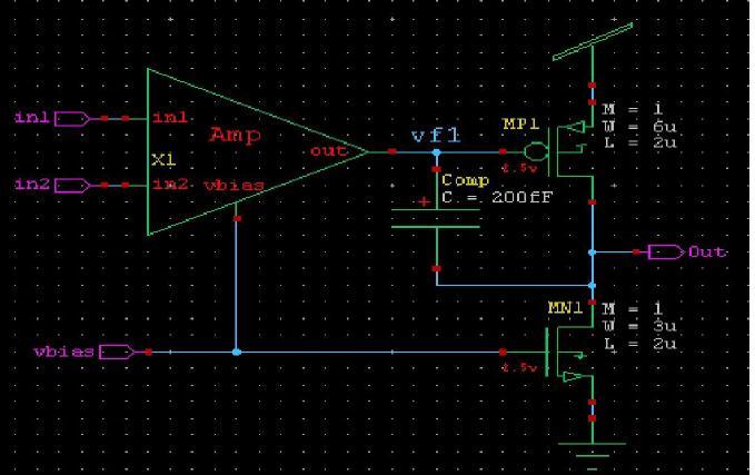
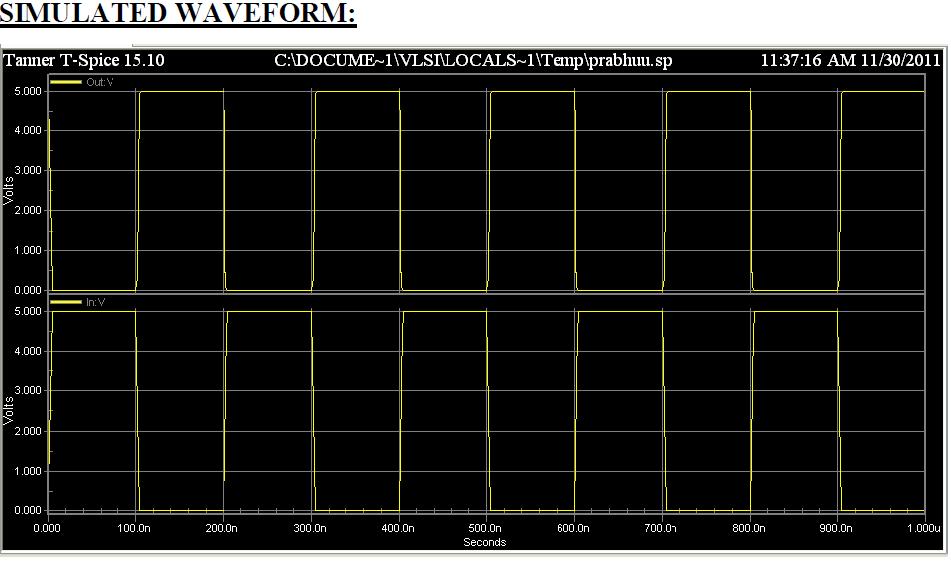
39 Experiment Number: 9 Title of the Experiment : DESIGN OF A 10 BIT NUMBER CONTROLLED OSCILLATOR Date of the experiment : OBJECTIVE OF THE EXPERIMENT To perform the functional verification of the design of a 10 bit number controlled oscillator through schematic entry. FACILITIES REQUIRED AND PROCEDURE a) Facilities required to do the experiment S.No. SOFTWARE REQUIREMENTS Quantity 1 S-Edit using CadanceTool 1 b) Procedure for doing the experiment S.No Details of the step 1 Draw the schematic of CMOS Inverter using S-edit. 2 Perform Transient Analysis of the CMOS Inverter 3 Obtain the output waveform from W-edit 4 Obtain the spice code using T-edit. SCHEMATIC DIAGRAM: 39

40 RESULT: Thus the the functional verification of the design of a 10 bit number controlled oscillator through schematic entry. 40
41 Experiment Number: 10 Title of The Experiment : AUTOMATIC LAYOUT GENERATION Date of the experiment : OBJECTIVE OF THE EXPERIMENT To generate the Layout from the schematic using the Tanner tool and verify the layout using simulation. FACILITIES REQUIRED AND PROCEDURE a) Facilities required to do the experiment S.No. SOFTWARE REQUIREMENTS Quantity 1 S-Edit, L-Edit using Tanner Tool 1 b) Procedure for doing the experiment S.No Details of the step 1 Draw the schematic using S Edit and verify the output in W Edit. 2 Extract the schematic and store it in another location 3 Open the L Edit, open the design in Ring VCO 4 Create the new cell 5 Open the schematic file (.sdl) using the SDL Navigator 6 Do the necessary connections as per the design. 7 Name the ports and check the design for the DRC Rules 8 Locate the Destination file in the setup Extract window and extract the layout. 9 Include the Library and the print voltage statements in the net list which is obtained. 10 Verify the layout design using W Edit. 41

42 SCHEMATIC DIAGRAM: 42
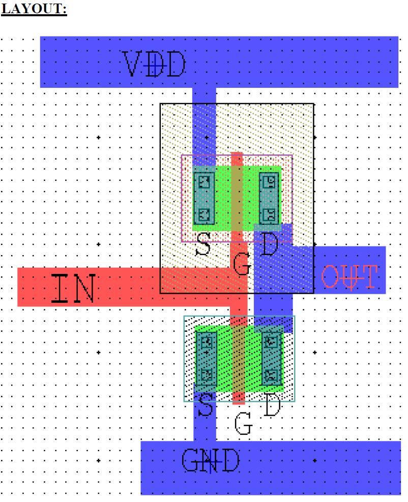
43 43

44 RESULT: Thus the the Layout from the schematic using the Cadance tool and verify the layout using simulation and the output also verified successfully. 44
45 BEYOND THE SYLLABUS 45
46 Experiment Number: 11 Title of the experiment : IMPLEMENTATION OF FLIP-FLOPS Date of the experiment : OBJECTIVE OF THE EXPERIMENT To implement Flip-flops using Verilog HDL. FACILITIES REQUIRED AND PROCEDURE a) Facilities required to do the experiment S.No. SOFTWARE REQUIREMENTS Quantity 1 Xilinx Project navigator ISE b) Procedure for doing the experiment S.No Details of the step 1 Double click the project navigator and select the option File-New project. 2 Give the project name. 3 Select Verilog module. 4 Type your verilog coding. 5 Check for syntax. 6 Select the new source of test bench waveform 7 Choose behavioral simulation and simulate it by xilinx ISE simulator. 8 Verify the output. 46
47 c) Verilog coding: PROGRAM: D Flip-Flop: // Module Name: DFF module DFF(Clock, Reset, d, q); input Clock; input Reset; input d; output q; reg q; always@(posedge Clock or negedge Reset) if (~Reset) q=1'b0; else q=d; endmodule T Flip-Flop: // Module Name: TFF module TFF(Clock, Reset, t, q); input Clock; input Reset; input t; output q; reg q; always@(posedge Clock, negedge Reset) if(~reset) q=0; else if (t) q=~q; 47
48 else q=q; endmodule JK Flip-Flop: Program: // Module Name: JKFF module JKFF(Clock, Reset, j, k, q); input Clock; input Reset; input j; input k; output q; reg q; Clock, negedge Reset) if(~reset)q=0; else begin case({j,k}) 2'b00: q=q; 2'b01: q=0; 2'b10: q=1; 2'b11: q=~q; endcase end endmodule RESULT: Thus the flip-flops program was implemented using tools and the output also verified successfully. 48
49 Experiment Number: 12 Title of the experiment : IMPLEMENTATION OF COUNTERS Date of the experiment : OBJECTIVE OF THE EXPERIMENT To implement Counters using Verilog HDL. FACILITIES REQUIRED AND PROCEDURE a) Facilities required to do the experiment S.No. SOFTWARE REQUIREMENTS Quantity 1 Xilinx Project navigator ISE b) Procedure for doing the experiment S.No Details of the step 1 Double click the project navigator and select the option File-New project. 2 Give the project name. 3 Select Verilog module. 4 Type your verilog coding. 5 Check for syntax. 6 Select the new source of test bench waveform 7 Choose behavioral simulation and simulate it by xilinx ISE simulator. 8 Verify the output. 49
50 c) Verilog coding: PROGRAM: 2- Bit Counter: // Module Name: Count2Bit module Count2Bit(Clock, Clear, out); input Clock; input Clear; output [1:0] out; reg [1:0]out; Clock, negedge Clear) if((~clear) (out>=4))out=2'b00; else out=out+1; endmodule RESULT: Thus the counters program was implemented using tools and the output also verified successfully. 50
51 Experiment Number: 13 Title of the experiment : IMPLEMENTATION OF REGISTERS Date of the experiment : OBJECTIVE OF THE EXPERIMENT To implement Registers using Verilog HDL. FACILITIES REQUIRED AND PROCEDURE a) Facilities required to do the experiment S.No. SOFTWARE REQUIREMENTS Quantity 1 Xilinx Project navigator ISE b) Procedure for doing the experiment S.No Details of the step 1 Double click the project navigator and select the option File-New project. 2 Give the project name. 3 Select Verilog module. 4 Type your verilog coding. 5 Check for syntax. 6 Select the new source of test bench waveform 7 Choose behavioral simulation and simulate it by xilinx ISE simulator. 8 Verify the output. 51
52 c) Verilog coding: PROGRAM: 2 Bit Register: // Module Name: Reg2Bit module Reg2Bit(Clock, Clear, in, out); input Clock; input Clear; input [0:1] in; output [0:1] out; reg [0:1] out; always@(posedge Clock, negedge Clear) if(~clear) out=2'b00; else out=in; endmodule RESULT: Thus the Registers program was implemented using tools and the output also verified successfully. 52
53 VIVA VOCE QUESTION &ANSWERS 1.What are four generations of Integration Circuits? 1)SSI (Small Scale Integration) 2)MSI (Medium Scale Integration) 3)LSI (Large Scale Integration) 4) VLSI (Very Large Scale Integration) 2. Give the advantages of IC? 1)Size is less 2)High Speed 3)Less Power Dissipation 3. Give the variety of Integrated Circuits? 1)More Specialized Circuits 2) Application Specific Integrated Circuits(ASICs) Systems-On-Chips 4. Give the basic process for IC fabrication? Silicon wafer Preparation, Epitaxial Growth, Oxidation, Photolithography, Diffusion Ion Implantation, Isolation technique, Metallization, Assembly processing & Packaging 5. What are the various Silicon wafer Preparation? Crystal growth & doping, Ingot trimming & grinding, Ingot slicing, Wafer polishing & etching, Wafer cleaning. 6. Different types of oxidation? Dry & Wet Oxidation 7. What is the transistors CMOS technology provides? n-type transistors & p-type transistors. 8. What are the different layers in MOS transistors? Drain, Source & Gate 9. What is Enhancement mode transistor? The device that is normally cut-off with zero gate bias. 10. What is Depletion mode Device? The Device that conduct with zero gate bias. 11. When the channel is said to be pinched off? If a large Vds is applied this voltage with deplete the Inversion layer.this Voltage 53
54 effectively pinches off the channel near the drain. 12. Give the different types of CMOS process? p-well process, n-well process, Silicon- On-Insulator Process, Twin- tub Process 13. What are the steps involved in twin-tub process? Tub Formation, Thin-oxide Construction, Source & Drain Implantation, Contact cut definition, Metallization. 14. What are the advantages of Silicon-on-Insulator process? No Latch-up, Due to absence of bulks transistor structures are denser than bulk silicon. 15. Define Short Channel devices? Transistors with Channel length less than 3-5 microns are termed as Short channel devices. With short channel devices the ratio between the lateral & vertical dimensions are reduced. Non- Saturated Region Saturated Region 16. Define Threshold voltage in CMOS? The Threshold voltage, VT for a MOS transistor can be defined as the voltage applied between the gate and the source of the MOS transistor below which the drain to source current, IDS effectively drops to zero. 17. What is Body effect? The threshold voltage VT is not a constant w. r. to the voltage difference between the substrate and the source of MOS transistor. This effect is called substrate-bias effect or body effect. 18. What is Verilog? Verilog is a general purpose hardware descriptor language. It is similar in syntax to the C programming language. It can be used to model a digital system at many levels of abstraction ranging from the algorithmic level to the switch level. 54
55 19. What are the various modeling used in Verilog 1. Gate-level modeling 2. Data-flow modeling 3. Switch-level modeling 4. Behavioral modeling 20. What is the structural gate-level modeling? Structural modeling describes a digital logic networks in terms of the components that make up the system. Gate-level modeling is based on using primitive logic gates and specifying how they are wired together. 21. What is Switch-level modeling? Verilog allows switch-level modeling that is based on the behavior of MOSFETs.Digital circuits at the MOS-transistor level are described using the MOSFET switches. 22. What are identifiers? Identifiers are names of modules, variables and other objects that we can reference in the design. Identifiers consists of upper and lower case letters, digits 0 through 9, the underscore character(_) and the dollar sign($). It must be a single group of characters. Examples: A014, a,b, in_o, s_out 55
 DEPT OF ECE EC6612 -VLSI DESIGN LABORATORY MANUAL (REGULATION-2013) LAB MANUAL DEPARTMENT OF ECE NAME: REGISTER NUMBER: YEAR/SEM.: ACADEMIC YEAR: 2015-2016 DEPT OF ECE EC6612 -VLSI DESIGN LABORATORY MANUAL
 PAGE NO: EXP NO: 1A SIMULATION OF HALF ADDER AND FULL ADDER. DATE: AIM: To design, simulate and synthesize the Half adder and Full adder. TOOLS REQUIRED: SOFTWARE: XILINX ISE 9.1i ALGORITHM: 1. Start the
Department of Computer Science & Engineering. Lab Manual DIGITAL LAB. Class: 2nd yr, 3rd sem SYLLABUS
 Department of Computer Science & Engineering Lab Manual 435 DIGITAL LAB Class: 2nd yr, 3rd sem SYLLABUS. Verification of Boolean theorems using digital logic gates. 2. Design and implementation of code
QUESTION BANK DEPARTMENT OF ECE
 QUESTION BANK DEPARTMENT OF ECE YEAR: III SEM: VI SUBJECTCODE:EC2354 SUBJECT NAME:VLSI DESIGN Prepared by V.GUNASUNDARI/AP 1.List the advantages of SOI CMOS process Denser transistor structures are possible.
UNIT V: SPECIFICATION USING VERILOG HDL
 UNIT V: SPECIFICATION USING VERILOG HDL PART -A (2 Marks) 1. What are identifiers? Identifiers are names of modules, variables and other objects that we can reference in the design. Identifiers consists
N-input EX-NOR gate. N-output inverter. N-input NOR gate
 Hardware Description Language HDL Introduction HDL is a hardware description language used to design and document electronic systems. HDL allows designers to design at various levels of abstraction. It
ESE 570 Cadence Lab Assignment 2: Introduction to Spectre, Manual Layout Drawing and Post Layout Simulation (PLS)
") ESE 570 Cadence Lab Assignment 2: Introduction to Spectre, Manual Layout Drawing and Post Layout Simulation (PLS) Objective Part A: To become acquainted with Spectre (or HSpice) by simulating an inverter,
ESE 570 Cadence Lab Assignment 2: Introduction to Spectre, Manual Layout Drawing and Post Layout Simulation (PLS) Objective Part A: To become acquainted with Spectre (or HSpice) by simulating an inverter,
Federal Urdu University of Arts, Science and Technology, Islamabad VLSI SYSTEM DESIGN. Prepared By: Engr. Yousaf Hameed.
 VLSI SYSTEM DESIGN Prepared By: Engr. Yousaf Hameed Lab Engineer BASIC ELECTRICAL & DIGITAL SYSTEMS LAB DEPARTMENT OF ELECTRICAL ENGINEERING VLSI System Design 1 LAB 01 Schematic Introduction to DSCH and
Digital Design with FPGAs. By Neeraj Kulkarni
 Digital Design with FPGAs By Neeraj Kulkarni Some Basic Electronics Basic Elements: Gates: And, Or, Nor, Nand, Xor.. Memory elements: Flip Flops, Registers.. Techniques to design a circuit using basic
Spiral 2-8. Cell Layout
 2-8.1 Spiral 2-8 Cell Layout 2-8.2 Learning Outcomes I understand how a digital circuit is composed of layers of materials forming transistors and wires I understand how each layer is expressed as geometric
ICAL ENG LAB MANUAL EC6612- VLSI DESIGN LABORATORY. Dharmapuri : B.E. ECE. Branch EC6612 VLSI DESIGN LAB
 1 Dharmapuri 636 703 LAB MANUAL Regulation : 2013 Branch : B.E. ECE Year & Semester : III Year / VI Semester EC6612- VLSI DESIGN LABORATORY ICAL ENG 2 ANNA UNIVERSITY CHENNAI Regulation 2013 FPGA BASED
FPGA Design Challenge :Techkriti 14 Digital Design using Verilog Part 1
 FPGA Design Challenge :Techkriti 14 Digital Design using Verilog Part 1 Anurag Dwivedi Digital Design : Bottom Up Approach Basic Block - Gates Digital Design : Bottom Up Approach Gates -> Flip Flops Digital
DIGITAL SYSTEM DESIGN
 DIGITAL SYSTEM DESIGN Prepared By: Engr. Yousaf Hameed Lab Engineer BASIC ELECTRICAL & DIGITAL SYSTEMS LAB DEPARTMENT OF ELECTRICAL ENGINEERING Digital System Design 1 Name: Registration No: Roll No: Semester:
Lab. Course Goals. Topics. What is VLSI design? What is an integrated circuit? VLSI Design Cycle. VLSI Design Automation
 Course Goals Lab Understand key components in VLSI designs Become familiar with design tools (Cadence) Understand design flows Understand behavioral, structural, and physical specifications Be able to
PINE TRAINING ACADEMY
 PINE TRAINING ACADEMY Course Module A d d r e s s D - 5 5 7, G o v i n d p u r a m, G h a z i a b a d, U. P., 2 0 1 0 1 3, I n d i a Digital Logic System Design using Gates/Verilog or VHDL and Implementation
Design rule illustrations for the AMI C5N process can be found at:
 Cadence Tutorial B: Layout, DRC, Extraction, and LVS Created for the MSU VLSI program by Professor A. Mason and the AMSaC lab group. Revised by C Young & Waqar A Qureshi -FS08 Document Contents Introduction
LABORATORY MANUAL VLSI DESIGN LAB EE-330-F
 LABORATORY MANUAL VLSI DESIGN LAB EE-330-F (VI th Semester) Prepared By: Vikrant Verma B. Tech. (ECE), M. Tech. (ECE) Department of Electrical & Electronics Engineering BRCM College of Engineering & Technology
Computer Architecture (TT 2012)
") Computer Architecture (TT 2012) The Register Transfer Level Daniel Kroening Oxford University, Computer Science Department Version 1.0, 2011 Outline Reminders Gates Implementations of Gates Latches, Flip-flops
Computer Architecture (TT 2012) The Register Transfer Level Daniel Kroening Oxford University, Computer Science Department Version 1.0, 2011 Outline Reminders Gates Implementations of Gates Latches, Flip-flops
FACULTY OF ENGINEERING MULTIMEDIA UNIVERSITY LAB SHEET DIGITAL INTEGRATED CIRCUIT
 FACULTY OF ENGINEERING MULTIMEDIA UNIVERSITY LAB SHEET DIGITAL INTEGRATED CIRCUIT DIC1: Schematic Design Entry, Simulation & Verification DIC2: Schematic Driven Layout Drawing (SDL) Design Rule Check (DRC)
CMOS Design Lab Manual
 CMOS Design Lab Manual Developed By University Program Team CoreEl Technologies (I) Pvt. Ltd. 1 Objective Objective of this lab is to learn the Mentor Graphics HEP2 tools as well learn the flow of the
Circuit Design and Simulation with VHDL 2nd edition Volnei A. Pedroni MIT Press, 2010 Book web:
 Circuit Design and Simulation with VHDL 2nd edition Volnei A. Pedroni MIT Press, 2010 Book web: www.vhdl.us Appendix C Xilinx ISE Tutorial (ISE 11.1) This tutorial is based on ISE 11.1 WebPack (free at
A STUDY OF DESIGN TOOL - XILINX
 A STUDY OF DESIGN TOOL - XILINX 1. Open Xilinx Project Navigator from Start Menu Xilinx ISE Opens-up 2. Opening a New ProjectSelect New Project from File Menu The below window opensup Enter the Project
ENGN 1630: CPLD Simulation Fall ENGN 1630 Fall Simulating XC9572XLs on the ENGN1630 CPLD-II Board Using Xilinx ISim
 ENGN 1630 Fall 2018 Simulating XC9572XLs on the ENGN1630 CPLD-II Board Using Xilinx ISim You will use the Xilinx ISim simulation software for the required timing simulation of the XC9572XL CPLD programmable
INSTITUTE OF AERONAUTICAL ENGINEERING Dundigal, Hyderabad ELECTRONICS AND COMMUNICATIONS ENGINEERING
 INSTITUTE OF AERONAUTICAL ENGINEERING Dundigal, Hyderabad - 00 0 ELECTRONICS AND COMMUNICATIONS ENGINEERING QUESTION BANK Course Name : DIGITAL DESIGN USING VERILOG HDL Course Code : A00 Class : II - B.
Chennai Institute of Technology Sarathy Nagar, Pudupedu, Kundrathur, Chennai Department of Electronics and Communication Engineering
 Ex. No. 6 Date: CARRY SELECT ADDER Aim: To simulate and synthesis Carry Select Adder using Verilog HDL Software tools Required: Theory: Synthesis tool: Xilinx ISE. Simulation tool: Project navigator Simulator
CSE 591: Advanced Hardware Design and Verification (2012 Spring) LAB #0
 LAB #0") Lab 0: Tutorial on Xilinx Project Navigator & ALDEC s Active-HDL Simulator CSE 591: Advanced Hardware Design and Verification Assigned: 01/05/2011 Due: 01/19/2011 Table of Contents 1 Overview... 2 1.1
Lab 0: Tutorial on Xilinx Project Navigator & ALDEC s Active-HDL Simulator CSE 591: Advanced Hardware Design and Verification Assigned: 01/05/2011 Due: 01/19/2011 Table of Contents 1 Overview... 2 1.1
Brief Introduction of Cell-based Design. Ching-Da Chan CIC/DSD
 Brief Introduction of Cell-based Design Ching-Da Chan CIC/DSD 1 Design Abstraction Levels SYSTEM MODULE + GATE CIRCUIT S n+ G DEVICE n+ D 2 Full Custom V.S Cell based Design Full custom design Better patent
St.MARTIN S ENGINEERING COLLEGE Dhulapally, Secunderabad
 St.MARTIN S ENGINEERING COLLEGE Dhulapally, Secunderabad-500 014 Subject: Digital Design Using Verilog Hdl Class : ECE-II Group A (Short Answer Questions) UNIT-I 1 Define verilog HDL? 2 List levels of
Verilog Fundamentals. Shubham Singh. Junior Undergrad. Electrical Engineering
 Verilog Fundamentals Shubham Singh Junior Undergrad. Electrical Engineering VERILOG FUNDAMENTALS HDLs HISTORY HOW FPGA & VERILOG ARE RELATED CODING IN VERILOG HDLs HISTORY HDL HARDWARE DESCRIPTION LANGUAGE
VLSI Lab Tutorial 3. Virtuoso Layout Editing Introduction
 VLSI Lab Tutorial 3 Virtuoso Layout Editing Introduction 1.0 Introduction The purpose of this lab tutorial is to guide you through the design process in creating a custom IC layout for your CMOS inverter
MLR Institute of Technology
 MLR Institute of Technology Laxma Reddy Avenue, Dundigal, Quthbullapur (M), Hyderabad 500 043 Course Name Course Code Class Branch ELECTRONICS AND COMMUNICATIONS ENGINEERING QUESTION BANK : DIGITAL DESIGN
Verilog Design Entry, Synthesis, and Behavioral Simulation
 ------------------------------------------------------------- PURPOSE - This lab will present a brief overview of a typical design flow and then will start to walk you through some typical tasks and familiarize
6. Latches and Memories
 6 Latches and Memories This chapter . RS Latch The RS Latch, also called Set-Reset Flip Flop (SR FF), transforms a pulse into a continuous state. The RS latch can be made up of two interconnected
Actel Libero TM Integrated Design Environment v2.3 Structural Schematic Flow Design Tutorial
 Actel Libero TM Integrated Design Environment v2.3 Structural Schematic Flow Design Tutorial 1 Table of Contents Design Flow in Libero TM IDE v2.3 Step 1 - Design Creation 3 Step 2 - Design Verification
: : (91-44) (Office) (91-44) (Residence)
 (Office) (91-44) (Residence)") Course: VLSI Circuits (Video Course) Faculty Coordinator(s) : Prof. S. Srinivasan Department of Electrical Engineering Indian Institute of Technology Madras Chennai 600036 Email Telephone : srinis@iitm.ac.in,
Course: VLSI Circuits (Video Course) Faculty Coordinator(s) : Prof. S. Srinivasan Department of Electrical Engineering Indian Institute of Technology Madras Chennai 600036 Email Telephone : srinis@iitm.ac.in,
Lab 6 : Introduction to Verilog
 Lab 6 : Introduction to Verilog Name: Sign the following statement: On my honor, as an Aggie, I have neither given nor received unauthorized aid on this academic work 1 Objective The main objective of
After opening the Programs> Xilinx ISE 8.2i > Project Navigator, you will come to this screen as start-up.
 After opening the Programs> Xilinx ISE 8.2i > Project Navigator, you will come to this screen as start-up. Start with a new project. Enter a project name and be sure to select Schematic as the Top-Level
and 32 bit for 32 bit. If you don t pay attention to this, there will be unexpected behavior in the ISE software and thing may not work properly!
 This tutorial will show you how to: Part I: Set up a new project in ISE 14.7 Part II: Implement a function using Schematics Part III: Simulate the schematic circuit using ISim Part IV: Constraint, Synthesize,
Verilog Tutorial (Structure, Test)
") Digital Circuit Design and Language Verilog Tutorial (Structure, Test) Chang, Ik Joon Kyunghee University Hierarchical Design Top-down Design Methodology Bottom-up Design Methodology Module START Example)
Digital Circuit Design and Language Verilog Tutorial (Structure, Test) Chang, Ik Joon Kyunghee University Hierarchical Design Top-down Design Methodology Bottom-up Design Methodology Module START Example)
ENEE245 Digital Circuits and Systems Lab Manual
 ENEE245 Digital Circuits and Systems Lab Manual Department of Engineering, Physical & Computer Sciences Montgomery College Version 1.1 Copyright Prof. Lan Xiang (Do not distribute without permission) 1
TUTORIAL II ECE 555 / 755 Updated on September 11 th 2006 CADENCE LAYOUT AND PARASITIC EXTRACTION
 TUTORIAL II ECE 555 / 755 Updated on September 11 th 2006 CADENCE LAYOUT AND PARASITIC EXTRACTION After finishing a schematic of your design (Tutorial-I), the next step is creating masks which are for
Cadence Virtuoso Schematic Design and Circuit Simulation Tutorial
 Cadence Virtuoso Schematic Design and Circuit Simulation Tutorial Introduction This tutorial is an introduction to schematic capture and circuit simulation for ENGN1600 using Cadence Virtuoso. These courses
ENEE245 Digital Circuits and Systems Lab Manual
 ENEE245 Digital Circuits and Systems Lab Manual Department of Engineering, Physical & Computer Sciences Montgomery College Modified Fall 2017 Copyright Prof. Lan Xiang (Do not distribute without permission)
DESIGN STRATEGIES & TOOLS UTILIZED
 CHAPTER 7 DESIGN STRATEGIES & TOOLS UTILIZED 7-1. Field Programmable Gate Array The internal architecture of an FPGA consist of several uncommitted logic blocks in which the design is to be encoded. The
Xilinx Tutorial Basic Walk-through
 Introduction to Digital Logic Design with FPGA s: Digital logic circuits form the basis of all digital electronic devices. FPGAs (Field Programmable Gate Array) are large programmable digital electronic
ECE 4514 Digital Design II. Spring Lecture 2: Hierarchical Design
 ECE 4514 Digital Design II Spring 2007 Abstraction in Hardware Design Remember from last lecture that HDLs offer a textual description of a netlist. Through abstraction in the HDL, we can capture more
FPGA Design Flow 1. All About FPGA
 FPGA Design Flow 1 In this part of tutorial we are going to have a short intro on FPGA design flow. A simplified version of FPGA design flow is given in the flowing diagram. FPGA Design Flow 2 FPGA_Design_FLOW
WINTER 14 EXAMINATION Subject Code: Model Answer Page No: / N
 Important Instructions to examiners: 1) The answers should be examined by key words and not as word-to-word as given in the model answer scheme. 2) The model answer and the answer written by candidate
Cadence Tutorial A: Schematic Entry and Functional Simulation Created for the MSU VLSI program by Andrew Mason and the AMSaC lab group.
 Cadence Tutorial A: Schematic Entry and Functional Simulation Created for the MSU VLSI program by Andrew Mason and the AMSaC lab group. Revision Notes: Aug. 2003 update and edit A. Mason add intro/revision/contents
Tutorial: Working with the Xilinx tools 14.4
 Tutorial: Working with the Xilinx tools 14.4 This tutorial will show you how to: Part I: Set up a new project in ISE Part II: Implement a function using Schematics Part III: Implement a function using
Course Batch Semester Subject Code Subject Name. B.E-Marine Engineering B.E- ME-16 III UBEE307 Integrated Circuits
 Course Batch Semester Subject Code Subject Name B.E-Marine Engineering B.E- ME-16 III UBEE307 Integrated Circuits Part-A 1 Define De-Morgan's theorem. 2 Convert the following hexadecimal number to decimal
Logic Circuits II ECE 2411 Thursday 4:45pm-7:20pm. Lecture 3
 Logic Circuits II ECE 2411 Thursday 4:45pm-7:20pm Lecture 3 Lecture 3 Topics Covered: Chapter 4 Discuss Sequential logic Verilog Coding Introduce Sequential coding Further review of Combinational Verilog
Revision: February 27, E Main Suite D Pullman, WA (509) Voice and Fax
 Voice and Fax") Xilinx ISE WebPACK Schematic Capture Tutorial Revision: February 27, 2010 215 E Main Suite D Pullman, WA 99163 (509) 334 6306 Voice and Fax Overview This tutorial provides instruction for using the Xilinx
Xilinx ISE WebPACK Schematic Capture Tutorial Revision: February 27, 2010 215 E Main Suite D Pullman, WA 99163 (509) 334 6306 Voice and Fax Overview This tutorial provides instruction for using the Xilinx
Digital Circuit Design and Language. Datapath Design. Chang, Ik Joon Kyunghee University
 Digital Circuit Design and Language Datapath Design Chang, Ik Joon Kyunghee University Typical Synchronous Design + Control Section : Finite State Machine + Data Section: Adder, Multiplier, Shift Register
2IN35 VLSI Programming Lab Work Assignment 1: Hardware design using Verilog
 2IN35 VLSI Programming Lab Work Assignment 1: Hardware design using Verilog Hrishikesh Salunkhe, h.l.salunkhe@tue.nl, Alok Lele, a.lele@tue.nl April 28, 2015 1 Contents 1 Introduction 3 2 Hardware design
Lay ay ut Design g R ules
 HPTER 5: Layout esign Rules Introduction ny circuit physical mask layout must conform to a set of geometric constraints or rules called as Layout esign rules before it can be manufactured using particular
Virtuoso Layout Editor
 This tutorial will cover the basic steps involved in using the Cadence layout editor called Virtuoso, extracting layout, and running simulation on the layout. The inverter layout is used as an example
Xilinx Schematic Entry Tutorial
 Overview Xilinx Schematic Entry Tutorial Xilinx ISE Schematic Entry & Modelsim Simulation What is circuit simulation and why is it important? Complex designs, short design cycle Simultaneous system design
Graphics: Alexandra Nolte, Gesine Marwedel, Universität Dortmund. RTL Synthesis
 Graphics: Alexandra Nolte, Gesine Marwedel, 2003 Universität Dortmund RTL Synthesis Purpose of HDLs Purpose of Hardware Description Languages: Capture design in Register Transfer Language form i.e. All
TOPIC : Verilog Synthesis examples. Module 4.3 : Verilog synthesis
 TOPIC : Verilog Synthesis examples Module 4.3 : Verilog synthesis Example : 4-bit magnitude comptarator Discuss synthesis of a 4-bit magnitude comparator to understand each step in the synthesis flow.
CPLD Experiment 4. XOR and XNOR Gates with Applications
 CPLD Experiment 4 XOR and XNOR Gates with Applications Based on Xilinx ISE Design Suit 10.1 Department of Electrical & Computer Engineering Florida International University Objectives Materials Examining
Process technology and introduction to physical
 Neuromorphic Engineering II Lab 3, Spring 2014 1 Lab 3 March 10, 2014 Process technology and introduction to physical layout Today you will start to learn to use the Virtuoso layout editor XL which is
ELEC 204 Digital System Design LABORATORY MANUAL
 ELEC 204 Digital System Design LABORATORY MANUAL : Introductory Tutorial For Xilinx ISE Foundation v10.1 & Implementing XOR Gate College of Engineering Koç University Important Note: In order to effectively
FPGA Design Tutorial
 ECE 554 Digital Engineering Laboratory FPGA Design Tutorial Version 5.0 Fall 2006 Updated Tutorial: Jake Adriaens Original Tutorial: Matt King, Surin Kittitornkun and Charles R. Kime Table of Contents
Composite Layout CS/EE N-type from the top. N-type Transistor. Diffusion Mask. Polysilicon Mask
 Composite Layout CS/EE 6710 Introduction to Layout Inverter Layout Example Layout Design Rules Drawing the mask layers that will be used by the fabrication folks to make the devices Very different from
Chapter 6. CMOS Functional Cells
 Chapter 6 CMOS Functional Cells In the previous chapter we discussed methods of designing layout of logic gates and building blocks like transmission gates, multiplexers and tri-state inverters. In this
Why Should I Learn This Language? VLSI HDL. Verilog-2
 Verilog Why Should I Learn This Language? VLSI HDL Verilog-2 Different Levels of Abstraction Algorithmic the function of the system RTL the data flow the control signals the storage element and clock Gate
ECE 4514 Digital Design II. Spring Lecture 20: Timing Analysis and Timed Simulation
 ECE 4514 Digital Design II Lecture 20: Timing Analysis and Timed Simulation A Tools/Methods Lecture Topics Static and Dynamic Timing Analysis Static Timing Analysis Delay Model Path Delay False Paths Timing
Lecture 1: Introduction Course arrangements Recap of basic digital design concepts EDA tool demonstration
 TKT-1426 Digital design for FPGA, 6cp Fall 2011 http://www.tkt.cs.tut.fi/kurssit/1426/ Tampere University of Technology Department of Computer Systems Waqar Hussain Lecture Contents Lecture 1: Introduction
(ii) Simplify and implement the following SOP function using NOR gates:
 Simplify and implement the following SOP function using NOR gates:") DHANALAKSHMI COLLEGE OF ENGINEERING DEPARTMENT OF ELECTRONICS AND COMMUNICATION ENGINEERING EE6301 DIGITAL LOGIC CIRCUITS UNIT I NUMBER SYSTEMS AND DIGITAL LOGIC FAMILIES PART A 1. How can an OR gate be
DHANALAKSHMI COLLEGE OF ENGINEERING DEPARTMENT OF ELECTRONICS AND COMMUNICATION ENGINEERING EE6301 DIGITAL LOGIC CIRCUITS UNIT I NUMBER SYSTEMS AND DIGITAL LOGIC FAMILIES PART A 1. How can an OR gate be
TLL5000 Electronic System Design Base Module. Getting Started Guide, Ver 3.4
 TLL5000 Electronic System Design Base Module Getting Started Guide, Ver 3.4 COPYRIGHT NOTICE The Learning Labs, Inc. ( TLL ) All rights reserved, 2008 Reproduction in any form without permission is prohibited.
EE 330 Spring Laboratory 2: Basic Boolean Circuits
 EE 330 Spring 2013 Laboratory 2: Basic Boolean Circuits Objective: The objective of this experiment is to investigate methods for evaluating the performance of Boolean circuits. Emphasis will be placed
Q.1. Attempt any TEN of the following: (a) Define the term Noise Margins. Ans: [Define: 2 M]
![Q.1. Attempt any TEN of the following: (a) Define the term Noise Margins. Ans: [Define: 2 M]](/thumbs/90/102030632.jpg "Q.1. Attempt any TEN of the following: (a) Define the term Noise Margins. Ans: [Define: 2 M]") Subject Code: 17659 Model Answer Page 1 of 24 Important Instructions to examiners: 1) The answers should be examined by key words and not as word-to-word as given in the model answer scheme. 2) The model
Subject Code: 17659 Model Answer Page 1 of 24 Important Instructions to examiners: 1) The answers should be examined by key words and not as word-to-word as given in the model answer scheme. 2) The model
ECE 2300 Digital Logic & Computer Organization. More Sequential Logic Verilog
 ECE 2300 Digital Logic & Computer Organization Spring 2018 More Sequential Logic Verilog Lecture 7: 1 Announcements HW3 will be posted tonight Prelim 1 Thursday March 1, in class Coverage: Lectures 1~7
Hardware Modeling using Verilog Prof. Indranil Sengupta Department of Computer Science and Engineering Indian Institute of Technology, Kharagpur
 Hardware Modeling using Verilog Prof. Indranil Sengupta Department of Computer Science and Engineering Indian Institute of Technology, Kharagpur Lecture 01 Introduction Welcome to the course on Hardware
CHAPTER 12 ARRAY SUBSYSTEMS [ ] MANJARI S. KULKARNI
![CHAPTER 12 ARRAY SUBSYSTEMS [ ] MANJARI S. KULKARNI](/thumbs/76/73997056.jpg "CHAPTER 12 ARRAY SUBSYSTEMS [ ] MANJARI S. KULKARNI") CHAPTER 2 ARRAY SUBSYSTEMS [2.4-2.9] MANJARI S. KULKARNI OVERVIEW Array classification Non volatile memory Design and Layout Read-Only Memory (ROM) Pseudo nmos and NAND ROMs Programmable ROMS PROMS, EPROMs,
CHAPTER 2 ARRAY SUBSYSTEMS [2.4-2.9] MANJARI S. KULKARNI OVERVIEW Array classification Non volatile memory Design and Layout Read-Only Memory (ROM) Pseudo nmos and NAND ROMs Programmable ROMS PROMS, EPROMs,
CMOS Process Flow. Layout CAD Tools
 CMOS Process Flow See supplementary power point file for animated CMOS process flow (see class ece410 website and/or* http://www.multimedia.vt.edu/ee5545/): This file should be viewed as a slide show It
Lab 7 (Sections 300, 301 and 302) Prelab: Introduction to Verilog
 Prelab: Introduction to Verilog") Lab 7 (Sections 300, 301 and 302) Prelab: Introduction to Verilog Name: Sign the following statement: On my honor, as an Aggie, I have neither given nor received unauthorized aid on this academic work
Lab 7 (Sections 300, 301 and 302) Prelab: Introduction to Verilog Name: Sign the following statement: On my honor, as an Aggie, I have neither given nor received unauthorized aid on this academic work
101-1 Under-Graduate Project Digital IC Design Flow
 101-1 Under-Graduate Project Digital IC Design Flow Speaker: Ming-Chun Hsiao Adviser: Prof. An-Yeu Wu Date: 2012/9/25 ACCESS IC LAB Outline Introduction to Integrated Circuit IC Design Flow Verilog HDL
EE 1315 DIGITAL LOGIC LAB EE Dept, UMD
 EE 1315 DIGITAL LOGIC LAB EE Dept, UMD EXPERIMENT # 1: Logic building blocks The main objective of this experiment is to let you familiarize with the lab equipment and learn about the operation of the
Synthesis of Combinational and Sequential Circuits with Verilog
 Synthesis of Combinational and Sequential Circuits with Verilog What is Verilog? Hardware description language: Are used to describe digital system in text form Used for modeling, simulation, design Two
FPGA Programming Technology
 FPGA Programming Technology Static RAM: This Xilinx SRAM configuration cell is constructed from two cross-coupled inverters and uses a standard CMOS process. The configuration cell drives the gates of
EE 330 Laboratory 3 Layout, DRC, and LVS Fall 2015
 EE 330 Laboratory 3 Layout, DRC, and LVS Fall 2015 Contents Objective:... 2 Part 1 Creating a layout... 2 1.1 Run DRC Early and Often... 2 1.2 Create N active and connect the transistors... 3 1.3 Vias...
Introduction to CMOS VLSI Design (E158) Lab 4: Controller Design
 Lab 4: Controller Design") Harris Introduction to CMOS VLSI Design (E158) Lab 4: Controller Design The controller for your MIPS processor is responsible for generating the signals to the datapath to fetch and execute each instruction.
Harris Introduction to CMOS VLSI Design (E158) Lab 4: Controller Design The controller for your MIPS processor is responsible for generating the signals to the datapath to fetch and execute each instruction.
Introduction to ICs and Transistor Fundamentals
 Introduction to ICs and Transistor Fundamentals A Brief History 1958: First integrated circuit Flip-flop using two transistors Built by Jack Kilby at Texas Instruments 2003 Intel Pentium 4 mprocessor (55
Step 1: Downloading the source files
 Introduction: In this lab and in the remainder of the ELEC 2607 labs, you will be using the Xilinx ISE to enter and simulate the designs for your circuits. In labs 3 and 4, you will use ISE to compile
CPE/EE 427, CPE 527, VLSI Design I: Tutorial #2, Schematic Capture, DC Analysis, Transient Analysis (Inverter, NAND2)
") CPE/EE 427, CPE 527, VLSI Design I: Tutorial #2, Schematic Capture, DC Analysis, Transient Analysis (Inverter, NAND2) Joel Wilder, Aleksandar Milenkovic, ECE Dept., The University of Alabama in Huntsville
CPE/EE 427, CPE 527, VLSI Design I: Tutorial #2, Schematic Capture, DC Analysis, Transient Analysis (Inverter, NAND2) Joel Wilder, Aleksandar Milenkovic, ECE Dept., The University of Alabama in Huntsville
ECE 574: Modeling and Synthesis of Digital Systems using Verilog and VHDL. Fall 2017 Final Exam (6.00 to 8.30pm) Verilog SOLUTIONS
 Verilog SOLUTIONS") ECE 574: Modeling and Synthesis of Digital Systems using Verilog and VHDL Fall 2017 Final Exam (6.00 to 8.30pm) Verilog SOLUTIONS Note: Closed book no notes or other material allowed apart from the one
ECE 574: Modeling and Synthesis of Digital Systems using Verilog and VHDL Fall 2017 Final Exam (6.00 to 8.30pm) Verilog SOLUTIONS Note: Closed book no notes or other material allowed apart from the one
EE115C Digital Electronic Circuits. Tutorial 2: Hierarchical Schematic and Simulation
 EE115C Digital Electronic Circuits Tutorial 2: Hierarchical Schematic and Simulation The objectives are to become familiar with Virtuoso schematic editor, learn how to create the symbol view of basic primitives,
Design a three-input, two-output sequential digital circuit which functions as a digital locking mechanism. LOCK ALARM
 Department of Computing Course 112 Hardware First Year Laboratory Assignment Dates for the session 2005-2006: Hand out Date: 10 th January 2006 Hand in deadline (electronic and written report): 17.00 Monday
Introduction to WebPACK 5.2 for FPGAs. Using Xilinx WebPACK Software to Create FPGA Designs for the XSB-300E Board
 Introduction to WebPACK 5.2 for FPGAs Using Xilinx WebPACK Software to Create FPGA Designs for the XSB-300E Board Release date: 10/27/2003 All XS-prefix product designations are trademarks of XESS Corp.
UNIT IV CMOS TESTING
 UNIT IV CMOS TESTING 1. Mention the levels at which testing of a chip can be done? At the wafer level At the packaged-chip level At the board level At the system level In the field 2. What is meant by
EE 367 Logic Design Lab #1 Introduction to Xilinx ISE and the ML40X Eval Board Date: 1/21/09 Due: 1/28/09
 EE 367 Logic Design Lab #1 Introduction to Xilinx ISE and the ML40X Eval Board Date: 1/21/09 Due: 1/28/09 Lab Description Today s lab will introduce you to the Xilinx Integrated Software Environment (ISE)
Laboratory of Digital Circuits Design: Design, Implementation and Simulation of Digital Circuits Using Programmable Devices
 Internet Engineering Dr. Jarosław Sugier Laboratory of Digital Circuits Design: Design, Implementation and Simulation of Digital Circuits Using Programmable Devices This document presents software packages
Introduction to Verilog design. Design flow (from the book) Hierarchical Design. Lecture 2
 Hierarchical Design. Lecture 2") Introduction to Verilog design Lecture 2 ECE 156A 1 Design flow (from the book) ECE 156A 2 Hierarchical Design Chip Modules Cells Primitives A chip contain many modules A module may contain other modules
Introduction to Verilog design Lecture 2 ECE 156A 1 Design flow (from the book) ECE 156A 2 Hierarchical Design Chip Modules Cells Primitives A chip contain many modules A module may contain other modules
Graduate Institute of Electronics Engineering, NTU. FPGA Lab. Speaker : 鍾明翰 (CMH) Advisor: Prof. An-Yeu Wu Date: 2010/12/14 ACCESS IC LAB
 Advisor: Prof. An-Yeu Wu Date: 2010/12/14 ACCESS IC LAB") FPGA Lab Speaker : 鍾明翰 (CMH) Advisor: Prof. An-Yeu Wu Date: 2010/12/14 ACCESS IC LAB Objective In this Lab, you will learn the basic set-up and design methods of implementing your design by ISE 10.1. Create
FPGA Lab Speaker : 鍾明翰 (CMH) Advisor: Prof. An-Yeu Wu Date: 2010/12/14 ACCESS IC LAB Objective In this Lab, you will learn the basic set-up and design methods of implementing your design by ISE 10.1. Create
Speaker: Shao-Wei Feng Adviser: Prof. An-Yeu Wu Date: 2010/09/28
 99-1 Under-Graduate Project Verilog Simulation & Debugging Tools Speaker: Shao-Wei Feng Adviser: Prof. An-Yeu Wu Date: 2010/09/28 ACCESS IC LAB Outline Basic Concept of Verilog HDL Gate Level Modeling
Using Synplify Pro, ISE and ModelSim
 Using Synplify Pro, ISE and ModelSim VLSI Systems on Chip ET4 351 Rene van Leuken Huib Lincklaen Arriëns Rev. 1.2 The EDA programs that will be used are: For RTL synthesis: Synplicity Synplify Pro For
University of Hawaii EE 361L. Getting Started with Spartan 3E Digilent Basys2 Board. Lab 4.1
 University of Hawaii EE 361L Getting Started with Spartan 3E Digilent Basys2 Board Lab 4.1 I. Test Basys2 Board Attach the Basys2 board to the PC or laptop with the USB connector. Make sure the blue jumper
Revision Notes: July2004 Generate tutorial for single transistor analysis. Based on existing schematic entry tutorial developed for ECE410
 Cadence Analog Tutorial 1: Schematic Entry and Transistor Characterization Created for the MSU VLSI program by Professor A. Mason and the AMSaC lab group. Revision Notes: July2004 Generate tutorial for