Advanced SI Analysis Layout Driven Assembly. Tom MacDonald RF/SI Applications Engineer II
|
|
|
- Megan Sutton
- 5 years ago
- Views:
Transcription

1 Advanced SI Analysis Layout Driven Assembly 1 Tom MacDonald RF/SI Applications Engineer II
2 Abstract As the voracious appetite for technology continually grows, so too does the need for fast turn around times and efficient techniques for characterization. To improve timeliness of turns, ANSYS SI product suite offers new functionality to enhance the user experience with layout driven assembly. By combining HFSS for connectors and HFSS 3D Layout for boards, this methodology allows us to apply current best solving techniques to our problems for optimal turnaround time and accuracy. 2
3 Agenda Design Pressures Layout Driven Assembly Multiphyics Board Analysis SIwave Workflow Enhancements Q & A 3


4 Customer Pressures Energy Availability Time to Market Product Lifecycle Skilled Labor Margin for Error Competition Cost Constraints Lawsuits/Warranty Product Innovation Customer Expectations 4

5 Getting Product Designs Right Top Business Pressures Driving Product Design Improvement Frequent Design Changes Compressed Schedules Improving Quality Need to Innovate Additional New Features Source: Aberdeen Group, April 2011 Biggest Hurdles for Product Design Late-Design Problems Making Design Tradeoffs Frequent Design Changes Understanding Variation Skilled Technical Experts 5

6 ANSYS Electronics Desktop ANSYS, Inc. April 25, 2016

7 HFSS 3D Layout HFSS interface optimized for layout designs Stackup editor Trace, pads, vias bond wires, solder bumps and balls Same 3D accuracy of HFSS in automated design flow 7
8 Layout Driven Assembly 8
9 From Schematic Capture to Layout Driven Assembly The old way of analyzing a package system plus a board 32 bit DDR3 Board Package 9
10 Last year Package on Board Example Extract board in SIwave Export touchstone or dynamic link Extract package in HFSS Export touchstone or dynamic link Setup circuit schematic Run linear network analysis Challenge: requires the use of 2-3 software packages Next step: make a design change Next step challenges: Keep track of touchstone revs Making changes to SIwave design (no variables) 10
11 Present Day Package on Board Example Extract board using SIwave Extract package using HFSS Assemble full 3D model Run linear network analysis Benefit: requires the use 1 software package (Electronics Desktop) Next step: make a design change Benefits: No need to keep track of touchstone revs Layout interface enables parametric SIwave designs 11


12 System Verification Layout-Driven Assembly in ANSYS Electronics Desktop Place and connect components in Layout Simulate components with 3D accuracy ECAD and MCAD HFSS, SIwave, Q3D Apply automated circuit simulation to capture full system behavior Ease-of-use drive 3D simulation for design engineers 12

13 Layout Driven Assembly Reducing hands on engineering time Eliminate error prone system wiring 13

14 Virtual System Analysis with HFSS & SIwave Assemble ECAD & MCAD Select appropriate solver HFSS, SIwave or PlanarEM Connect TX/RX up within Schematic circuit analysis LNA IBIS & IBIS-AMI QuickEye & VerifEye HSPICE* PSPICE** *HSPICE solver requires Synopsys license; Nexxim supports HSPICE syntax ** Uses Nexxim solver with PSPICE syntax 14


15 3D Layout: Key Features HFSS 3D Dynamic Link in Layout 3D Placement and Positioning Improved Capacity and Layout Rendering Linear Network Analysis for Co-simulation LNA Setup and automated Net listing Component Models SIwave technology for large PCBs and packages SYZ Solver Geometry Checks 15
16 HFSS 3D Workflow Enhancements 16


17 Pin2Pin Utility.Net utility written to highlight layout automation Can be run with or without GUI Starts from.mcm or.brd 17


18 Cadence Automation ANSYS Automation Layout Simulation Democratization Time is best spent in design exploration and results analysis Unfortunately, a lot of time is spent preparing the model for simulation Automation of pre-processing would free up more of the engineer s time for design innovation ANSYS HFSS Simulation 18
19 Multiphysics Board Analysis 19

20 ANSYS Icepak 20


21 DC Heating SIwave for DC ECAD Translators User Interface I 2 R DC Analysis IRDrop Simulate Cadence Allegro BRD file SIwave User Interface DC Setup Voltage/Current Sources 21
 Import Power Loss Heat Sources and Sinks Mesh Options Temperature Boundary")
22 Two-way coupled Thermal Heating SIwave DC Icepak Thermal Board Layout File Setup File (optional) Materials and Stackup Voltages and Currents Power Loss Thermal Convergence Board Layout File Setup File (optional) Import Power Loss Heat Sources and Sinks Mesh Options Temperature Boundary Conditions 22


23 ANSYS Solutions for Pkg/PCB Thermal Management Design Challenges Thermal impact to IC Electric / Thermal Co-Analysis for PKG/PCB Automation of pre-processing would free up more of the engineer s time for design innovation Thermal impact for mechanical stress Optimization of power, weight, and thermal design requirements Electrical / Thermal Co-Simulation Thermal / Mechanical Co-Simulation 23


24 Mechanical Reliability Coupled Thermal/Stress Electronics assembly reliability ANSYS Mechanical can be used to predict stresses and deformation in the package during Flip Chip Attachment Crack Initiation and Crack Growth Thermal Cycling Solder Joint Reliability Shock Analysis Flip chip Attachment Solder Joint Reliability Layout Tool* ANSYS Mechanical Shock Analysis Crack 24


25 Mechanical: Electronics Assembly ANSYS Workbench Solder Bump Package/PCB 25
26 SIwave Workflow Enhancements 26
27 PowerArtist RTL RedHawk SoC Totem Analog/IP RH-CTA Thermal HFSS SIwave PSI Solver Q3D (TPA) Solver Q3D Extractor CPA Solver Nexxim HSPICE 27
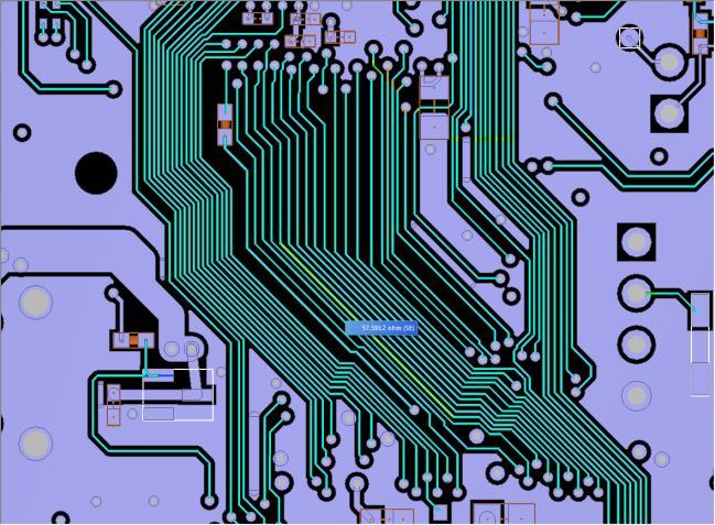
28 PowerArtist RedHawk Totem RH-CTA RTL SoC Analog/IP Thermal DC AC SYZ Plane Resonance Near/Far Field ALinks for EDA: ECAD Translation Loop Inductance Frequency Sweep Signal Net Analyzer Z o & X-talk Scans PI Advisor: Decoupling Optimization SI Circuit Analyses: IBIS, IBIS-AMI, Transient 28

29 SIwave SYZ Solver Integration into AEDT 3D Layout SIwave Solution Setups are now part of ANSYS Electronics Desktop 3D Layout Enables parametric solves Enables usage of Electromagnetics RSM Insert HFSS 3D Layout Design Add SIwave AC SYZ Solution 29


30 SIwave SYZ Solver Integration into AEDT 3D Layout SIwave Solution Setups are now part of ANSYS Electronics Desktop 3D Layout Enables parametric solves Enables usage of Electromagnetics RSM so that jobs can be submitted to a cluster 30

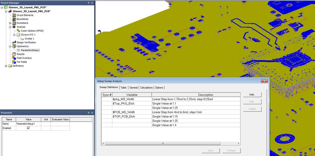
31 SIwave Parametric Design within AEDT 3D Layout 31
 solver is a 3D")

32 What is SIwave-CPA? The CPA (Chip-Package-Analysis) solver is a 3D full-wave, FEM based solver for fast and accurate extraction of RLC parasitics. It is optimized to analyze power and signal nets on packages 32
33 SIwave-CPA Automated.html reporting for partial and loop resistance/inductance The CPA solver is capable of producing per bump/ball resolution RLC extracted parasitics Visual Bar graph plotting is available for solderball/bump and Pin Groups Solver Net R (mω) Q3D (TPA) Flip-Chip PDN System L (nh) C (pf) Solve Time (minutes) Speed Up RAM (MB) RAM Reduction PDN A CPA PDN A x 210 4x Q3D PDN B (TPA) CPA PDN B x 210 4x 33
34 Solver Q3D (TPA) SIwave-CPA Wirebond Package PDN System Net R (mω) L (ph) C (pf) Solve Time (Hours) Speed Up RAM (GB) RAM Reduction PDN C CPA PDN C x 13 5x Q3D (TPA) PDN D CPA PDN D x 13 5x Solver Net Coupled Microstrip Lines R (mω) L (nh) C (pf) Solve Time (Minutes) Speed Up RAM (MB) RAM Reduction NPE Trace A CPA Trace A x 300 3x NPE Trace B CPA Trace B x 300 3x 34
 solver")
35 SIwave-Q3D (TPA) Improvements Added DC Adaptive Meshing Added the ability to use Pin Groups with Q3D (TPA) solver 35


36 SIwave Conformal Soldermasks Single Ended Zo Without Trace-Trace Coupling Without Conformal Soldermask Single Ended Zo With Trace-Trace Coupling Without Conformal Soldermask Single Ended Zo With Trace-Trace Coupling With Conformal Soldermask 36


37 Leadframe Editor Lead Frame Editor Creates SIwave & 3D Layout.anf Geometries Creates HFSS & Q3D.sat Geometries Lead Frame Editor SIwave QFP Package from Lead Frame Editor 37
38 Thank You 38
ANSYS, Inc. March 3, 2016 PCB 板极电热耦合分析及对电子设备热设计的影响
 1 2015 ANSYS, Inc. March 3, 2016 PCB 板极电热耦合分析及对电子设备热设计的影响 Printed Circuit Board Reliability Real world operating conditions = Multiphysics environment Electrical Reliability Power and Signal Integrity
ANSYS HFSS: Layout Driven Assembly in ANSYS Electronics Desktop
 Application Brief ANSYS HFSS: Layout Driven Assembly The ANSYS Electronics Desktop (AEDT) is an integrated environment with an easy-to-use interface that provides a streamlined workflow between ANSYS EM
Electromagnetics. R14 Update. Greg Pitner ANSYS, Inc. February 24, 2012
 Electromagnetics R14 Update Greg Pitner 1 HFSS Version 14 2 HFSS Overview Advanced Integrated Solver Technologies Finite Arrays with Domain Decomposition Hybrid solving: FEBI, IE Regions Physical Optics
HFSS 3D Components. Steve Rousselle, ANSYS. Build, Share, Conquer Release. Release ANSYS, Inc.
 HFSS 3D Components Build, Share, Conquer 2015.0 Release Steve Rousselle, ANSYS 1 2015 ANSYS, Inc. What is a 3D Component? Exploded View Assembly of 3D Components Device 2 2015 ANSYS, Inc. Introduction
Optimization of Modern Memory
 System Design, Verificationand and Optimization of Modern Memory Interfaces (DDR3) Santa Clara, Aug 23 rd 2011 Robert Myoung Sr. Application Engineer 1 Agenda Introduction ECAD Geometry Translation SI/PI
HFSS Solver-On-Demand for Package and PCB Characterization Using Cadence Greg Pitner
 HFSS Solver-On-Demand for Package and PCB Characterization Using Cadence Greg Pitner 1 ANSYS, Inc. September 14, Problem Statement Usually SI engineers extract only the package or the pcb due to the trade-offs
Realize Your Product Promise. DesignerRF
 Realize Your Product Promise DesignerRF Four-element antenna array showing current distribution and far-field gain, created in DesignerRF using layout editor and solved via HFSS with Solver on Demand technology
Package on Board Simulation with 3-D Electromagnetic Simulation
 White Paper Package on Board Simulation with 3-D Electromagnetic Simulation For many years, designers have taken into account the effect of package parasitics in simulation, from using simple first-order
HFSS Solver On Demand for Package and PCB Characterization Using Cadence. Greg Pitner
 HFSS Solver On Demand for Package and PCB Characterization Using Cadence Greg Pitner 1 Problem Statement Usually SI engineers extract only the package or the pcb due to the trade offs between capacity
Cadence Power Integrity Solutions For PCBs and IC Packages. May 2013
 Cadence Power Integrity Solutions For PCBs and IC Packages May 2013 Simultaneous Switching Noise (SSN) A Power Integrity Issue Design with decaps intentionally removed to demonstrate how poor PI performance
HFSS 14 Update for SI and RF Applications Markus Kopp Product Manager, Electronics ANSYS, Inc.
 HFSS 14 Update for SI and RF Applications Markus Kopp Product Manager, Electronics ANSYS, Inc. 1 ANSYS, Inc. September 21, Advanced Solvers: Finite Arrays with DDM 2 ANSYS, Inc. September 21, Finite Arrays
Realize Your Product Promise. Icepak
 Realize Your Product Promise Icepak ANSYS Icepak delivers powerful technology for electronics thermal management. Simulating high-performance electronics cooling readily solves challenges in this rapidly
Electrical optimization and simulation of your PCB design
 Electrical optimization and simulation of your PCB design Steve Gascoigne Senior Consultant at Mentor Graphics Zagreb, 10. lipnja 2015. Copyright CADCAM Group 2015 The Challenge of Validating a Design..
Ansys Designer RF Training Lecture 2: Introduction to the Designer GUI
 Ansys Designer RF Solutions for RF/Microwave Component and System Design 7. 0 Release Ansys Designer RF Training Lecture 2: Introduction to the Designer GUI Ansoft Designer Desktop Menu bar Toolbars Schematic
RTL2GDS Low Power Convergence for Chip-Package-System Designs. Aveek Sarkar VP, Technology Evangelism, ANSYS Inc.
 RTL2GDS Low Power Convergence for Chip-Package-System Designs Aveek Sarkar VP, Technology Evangelism, ANSYS Inc. Electronics Design Complexities Antenna Design and Placement Chip Low Power and Thermal
An Innovative Simulation Workflow for Debugging High-Speed Digital Designs using Jitter Separation
 An Innovative Simulation Workflow for Debugging High-Speed Digital Designs using Jitter Separation C. Chastang, A. Amédéo V. Poisson, P. Grison, F. Demuynck C. Gautier, F. Costa Thales Communications &
Using Sonnet in a Cadence Virtuoso Design Flow
 Using Sonnet in a Cadence Virtuoso Design Flow Purpose of this document: This document describes the Sonnet plug-in integration for the Cadence Virtuoso design flow, for silicon accurate EM modelling of
Allegro Sigrity SI Streamlining the creation of high-speed interconnect on digital PCBs and IC packages
 Streamlining the creation of high-speed interconnect on digital PCBs and IC packages The Cadence Allegro Sigrity signal integrity (SI) integrated high-speed design and analysis environment streamlines
Modern Memory Interfaces (DDR3) Design with ANSYS Virtual Prototype approach
 Design with ANSYS Virtual Prototype approach") Modern Memory Interfaces (DDR3) Design with ANSYS Virtual Prototype approach 1 ANSYS, Inc. Proprietary 2012 ANSYS, Inc. November 14, 2012 1-1 Agenda DDR Design Challenges How does simulation solve these
Modern Memory Interfaces (DDR3) Design with ANSYS Virtual Prototype approach 1 ANSYS, Inc. Proprietary 2012 ANSYS, Inc. November 14, 2012 1-1 Agenda DDR Design Challenges How does simulation solve these
Enabling SI Productivity Part 2. Venkatesh Seetharam Aaron Edwards
 Enabling SI Productivity Part 2 Venkatesh Seetharam Aaron Edwards 1 Problem Statement SI engineers use simulation software to squeeze the most performance out of their design. They will tend to focus on
Baseband IC Design Kits for Rapid System Realization
 Baseband IC Design Kits for Rapid System Realization Lanbing Chen Cadence Design Systems Engineering Director John Rowland Spreadtrum Communications SVP of Hardware Engineering Agenda How to Speed Up IC
Apache s Power Noise Simulation Technologies
 Enabling Power Efficient i Designs Apache s Power Noise Simulation Technologies 1 Aveek Sarkar VP of Support Apache Design Inc, A wholly owned subsidiary of ANSYS Trends in Today s Electronic Designs Low-power
A Modular Platform for Accurate Multi- Gigabit Serial Channel Validation
 A Modular Platform for Accurate Multi- Gigabit Serial Channel Validation Presenter: Andrew Byers Ansoft Corporation High Performance Electronics: Technical Challenges Faster data rates in increasingly
New Technologies in CST STUDIO SUITE CST COMPUTER SIMULATION TECHNOLOGY
 New Technologies in CST STUDIO SUITE 2016 Outline Design Tools & Modeling Antenna Magus Filter Designer 2D/3D Modeling 3D EM Solver Technology Cable / Circuit / PCB Systems Multiphysics CST Design Tools
Advances in 3D Simulations of Chip/Package/PCB Co-Design
 Advances in 3D Simulations of Chip/Package/PCB Co-Design Richard Sjiariel, CST AG Co-design environment Signal Integrity and timing Thermal analysis and stress Power Integrity and noise analysis EMC/EMI
Solving the challenges posed by Chip/Package/Board Co-Design
 Solving the challenges posed by Chip/Package/Board Co-Design Identify and locate sources of unwanted coupling Simulation link to EM: Critical Interconnect, Vias, Discontinuities, Embedded Passives, etc
Integrating ADS into a High Speed Package Design Process
 Integrating ADS into a High Speed Package Design Process Page 1 Group/Presentation Title Agilent Restricted Month ##, 200X Agenda High Speed SERDES Package Design Requirements Performance Factor and Design
Welcome. Joe Civello ADS Product Manager Agilent Technologies
 Welcome Joe Civello ADS Product Manager Agilent Technologies Agilent Technologies 2011 Agenda RF & microwave market trends & how Agilent EEsof is investing its R&D Multi-technology design with ADS 2011
HFSS 14 Update for SI and RF Applications. Presenter: Senior Application Engineer Jeff Tharp, Ph.D.
 HFSS 14 Update for SI and RF Applications Presenter: Senior Application Engineer Jeff Tharp, Ph.D. 1 Overview Advanced Integrated Solver Technologies Finite Arrays with Domain Decomposition Hybrid solving
Chip/Package/Board Design Flow
 Chip/Package/Board Design Flow EM Simulation Advances in ADS 2011.10 1 EM Simulation Advances in ADS2011.10 Agilent EEsof Chip/Package/Board Design Flow 2 RF Chip/Package/Board Design Industry Trends Increasing
Chip/Package/Board Interface Pathway Design and Optimization. Tom Whipple Product Engineering Architect November 2015
 Chip/Package/Board Interface Pathway Design and Optimization Tom Whipple Product Engineering Architect November 2015 Chip/package/board interface pathway design and optimization PCB design with Allegro
Contents. 1 CoreTech System Co., Ltd.
 Contents Advanced Support for Intelligent Workflow Improved User Interface 2 Expanded Gate Types.. 2 Enhanced Runner Wizard. 2 Customized Cooling Channel Templates. 3 Parameterized Mesh Generator... 3
Layer Stackup Wizard: Intuitive Pre-Layout Design
 Application Brief Layer Stackup Wizard: Intuitive Pre-Layout Design INTRODUCTION This Application Brief describes the Layer Stackup Wizard, a powerful utility within ANSYS SIwave for pre-layout stackup
Crossing the Chasm Between ECAD and CAE Virginia Manor Road, Suite 290, Beltsville MD
 Crossing the Chasm Between ECAD and CAE 1 Who is DfR Solutions? The Industry Leader in Quality-Reliability-Durability of Electronics 50 Fastest Growing Companies in the Electronics Industry - Inc Magazine
MRI Induced Heating of a Pacemaker. Peter Krenz, Application Engineer
 MRI Induced Heating of a Pacemaker Peter Krenz, Application Engineer 1 Problem Statement Electric fields generated during MRI exposure are dissipated in tissue of the human body resulting in a temperature
HFSS for ECAD: Package Modeling, MMIC and on-die extraction
 HFSS for ECAD: Package Modeling, MMIC and on-die extraction Alain Michel Technical Director, Europe 2010 ANSYS, Inc. All rights reserved. 1 ANSYS, Inc. Proprietary Agenda Introduction HFSS integrated Solver
ANSYS AIM 16.0 Overview. AIM Program Management
 1 2015 ANSYS, Inc. September 27, 2015 ANSYS AIM 16.0 Overview AIM Program Management 2 2015 ANSYS, Inc. September 27, 2015 Today s Simulation Challenges Leveraging simulation across engineering organizations
designs with signals operating in the multi-gigahertz (MGH) frequency range. It
 frequency range. It") DATASHEET ALLEGRO PCB SI GXL Cadence Allegro PCB SI GXL provides a virtual prototyping environment for designs with signals operating in the multi-gigahertz (MGH) frequency range. It offers a completely
DATASHEET ALLEGRO PCB SI GXL Cadence Allegro PCB SI GXL provides a virtual prototyping environment for designs with signals operating in the multi-gigahertz (MGH) frequency range. It offers a completely
Getting started. Starting Capture. To start Capture. This chapter describes how to start OrCAD Capture.
 Getting started 1 This chapter describes how to start OrCAD Capture. Starting Capture The OrCAD Release 9 installation process puts Capture in the \PROGRAM FILES\ORCAD\CAPTURE folder, and adds Pspice Student
Stacked IC Analysis Modeling for Power Noise Impact
 Si2 Open3D Kick-off Meeting June 7, 2011 Stacked IC Analysis Modeling for Power Noise Impact Aveek Sarkar Vice President Product Engineering & Support Stacked IC Design Needs Implementation Electrical-,
Appendix P. Multi-Physics Simulation Technology in NX. Christian Ruel (Maya Htt, Canada)
") 251 Appendix P Multi-Physics Simulation Technology in NX Christian Ruel (Maya Htt, Canada) 252 Multi-Physics Simulation Technology in NX Abstract As engineers increasingly rely on simulation models within
251 Appendix P Multi-Physics Simulation Technology in NX Christian Ruel (Maya Htt, Canada) 252 Multi-Physics Simulation Technology in NX Abstract As engineers increasingly rely on simulation models within
Thermo Mechanical Modeling of TSVs
 Thermo Mechanical Modeling of TSVs Jared Harvest Vamsi Krishna ih Yaddanapudi di 1 Overview Introduction to Through Silicon Vias (TSVs) Advantages of TSVs over wire bonding in packages Role of TSVs in
High Speed and High Power Connector Design
 High Speed and High Power Connector Design Taiwan User Conference 2014 Introduction High speed connector: Electrically small Using differential signaling Data rate >100Mbps High power connector: Static
Complete PCB Design Using OrCad Capture and Layout
 Complete PCB Design Using OrCad Capture and Layout By Kraig Mitzner Amsterdam Boston Heidelberg London New York Oxford Paris San Diego San Francisco Singapore Sydney Tokyo Newnes is an imprint of Elsevier
Simulation and Optimization in the wind energy industry
 Simulation and Optimization in the wind energy industry Numerical Simulation & Optimization www.ozeninc.com/optimization optimization@ozeninc.com Summary Why to use numerical simulations and optimization?
Chip Package System (CPS) Thermal Integrity Co-Analysis
 Thermal Integrity Co-Analysis") Chip Package System (CPS) Thermal Integrity Co-Analysis 尹国丽 / Principal Product Specialist Ansys 1 2017 ANSYS, Inc. Chip-Package-System Thermal Integrity Solution Chip-aware package and system thermal
Chip Package System (CPS) Thermal Integrity Co-Analysis 尹国丽 / Principal Product Specialist Ansys 1 2017 ANSYS, Inc. Chip-Package-System Thermal Integrity Solution Chip-aware package and system thermal
Wie entsteht ein EMV-Modell für eine integrierte Schaltung?
 Wie entsteht ein EMV-Modell für eine integrierte Schaltung? P. Schneider Overview Motivation Introduction Signal- and Power Integrity Simulation Tools Input Data Preparation gds2def & Power Annotation
Implementing Multi-Gigabit Serial Links in a System of PCBs
 Implementing Multi-Gigabit Serial Links in a System of PCBs Donald Telian April 2002 rev. 1.2 About the Author Donald Telian Technologist, Cadence Design Systems Donald has been involved in high-speed
Composites for JEC Conference. Zach Abraham ANSYS, Inc.
 Composites for JEC Conference Zach Abraham ANSYS, Inc. 1 Our Strategy Simulation-Driven Product Development Fluid Dynamics Structural Mechanics Explicit Dynamics Low-Frequency Electromagnetics High-Frequency
ANSYS Workbench for Process Compression and Scalability. Jiaping Zhang, Technical Service Engineer, Ansys Inc. Houston Office
 ANSYS Workbench for Process Compression and Scalability Jiaping Zhang, Technical Service Engineer, Ansys Inc. Houston Office Jiaping.Zhang@Ansys.com 1 Agenda 1. Ansys Workbench & Mechanical: An Introduction
Realize Your Product Promise HFSS
 Realize Your Product Promise HFSS Smart phone front view with electronic field displayed (left); back view with housing cut away to show internal geometry with electric field (right) Achieve high-frequency,
Toshiba Case Study RF Module Shrink (TransferJet TM )
") Toshiba Case Study RF Module Shrink (TransferJet TM ) These slides are an abridgement of two presentations given by Toshiba at the Zuken Innovation World (ZIW) conference held in Japan in 2012 and 2013.
Toshiba Case Study RF Module Shrink (TransferJet TM ) These slides are an abridgement of two presentations given by Toshiba at the Zuken Innovation World (ZIW) conference held in Japan in 2012 and 2013.
Optimum Placement of Decoupling Capacitors on Packages and Printed Circuit Boards Under the Guidance of Electromagnetic Field Simulation
 Optimum Placement of Decoupling Capacitors on Packages and Printed Circuit Boards Under the Guidance of Electromagnetic Field Simulation Yuzhe Chen, Zhaoqing Chen and Jiayuan Fang Department of Electrical
Finite Element Analysis using ANSYS Mechanical APDL & ANSYS Workbench
 Finite Element Analysis using ANSYS Mechanical APDL & ANSYS Workbench Course Curriculum (Duration: 120 Hrs.) Section I: ANSYS Mechanical APDL Chapter 1: Before you start using ANSYS a. Introduction to
2:1 MULTIPLEXER CHIP FOR PCI-EXPRESS ICS Description. Features. Block Diagram DATASHEET
 DATASHEET 2:1 MULTIPLEXER CHIP FOR PCI-EXPRESS ICS557-08 Description The ICS557-08 is a 2:1 multiplexer chip that allows the user to select one of the two HCSL (Host Clock Signal Level) or LVDS input pairs
What s New in HyperLynx 8.0
 What s New in HyperLynx 8.0 Copyright Mentor Graphics Corporation 2009 All Rights Reserved. Mentor Graphics, Board Station XE Flow, ViewDraw, Falcon Framework, IdeaStation, ICX and Tau are registered trademarks
APPENDIX-A INTRODUCTION TO OrCAD PSPICE
 220 APPENDIX-A INTRODUCTION TO OrCAD PSPICE 221 APPENDIX-A INTRODUCTION TO OrCAD PSPICE 1.0 INTRODUCTION Computer aided circuit analysis provides additional information about the circuit performance that
Automated Transient Thermal Analysis
 Automated Transient Thermal Analysis with ANSYS Icepak and Simplorer Using EKM Eric Lin Lalit Chaudhari Shantanu Bhide Vamsi Krishna Yaddanapudi 1 Overview Power Map Introduction Need for Chip-co Design
Cadence simulation technology for PCB design
 DATASHEET CADENCE SIMULATION FOR PCB DESIGN On larger designs especially, PCB design teams need fast and reliable simulation to achieve convergence. Cadence simulation technology for PCB design offers
A Practical Approach to Preventing Simultaneous Switching Noise and Ground Bounce Problems in IO Rings
 A Practical Approach to Preventing Simultaneous Switching Noise and Ground Bounce Problems in IO Rings Dr. Osman Ersed Akcasu, Jerry Tallinger, Kerem Akcasu OEA International, Inc. 155 East Main Avenue,
ASIC world. Start Specification Design Verification Layout Validation Finish
 AMS Verification Agenda ASIC world ASIC Industrial Facts Why Verification? Verification Overview Functional Verification Formal Verification Analog Verification Mixed-Signal Verification DFT Verification
MAX2009/MAX2010 Evaluation Kits
 19-2972; Rev 0; 9/03 MAX2009/MAX2010 Evaluation Kits General Description The MAX2009/MAX2010 evaluation kits (EV kits) simplify the evaluation of the MAX2009 and MAX2010. These kits are fully assembled
LiTE Design PORTFOLIO
 LiTE Design We Focus on scaling to new & latest technology in Electronic Design System, to develop & produce innovative products, services & solutions with our Potential that Exceeds the expectations of
Allegro PCB PDN Analysis User Guide
 Product Version 16.6 October 2012 Document Last Updated On: November 20, 2012 1991 2013 Cadence Design Systems, Inc. All rights reserved. Portions Apache Software Foundation, Sun Microsystems, Free Software
Simulation Advances. Antenna Applications
 Simulation Advances for RF, Microwave and Antenna Applications Presented by Martin Vogel, PhD Application Engineer 1 Overview Advanced Integrated Solver Technologies Finite Arrays with Domain Decomposition
Lecture 2: Introduction
 Lecture 2: Introduction v2015.0 Release ANSYS HFSS for Antenna Design 1 2015 ANSYS, Inc. Multiple Advanced Techniques Allow HFSS to Excel at a Wide Variety of Applications Platform Integration and RCS
Virtuoso System Design Platform Unified system-aware platform for IC and package design
 Unified system-aware platform for IC and package design The Cadence Virtuoso System Design Platform is a holistic, system-based solution that provides the functionality to drive simulation and LVS-clean
AXIEM EM Simulation/Verification of a Cadence Allegro PCB
 Application Example AXIEM EM Simulation/Verification of a Cadence Allegro PCB Overview This application example outlines the electromagnetic (EM) simulation and verification flow that exists between Cadence
ESE 570 Cadence Lab Assignment 2: Introduction to Spectre, Manual Layout Drawing and Post Layout Simulation (PLS)
") ESE 570 Cadence Lab Assignment 2: Introduction to Spectre, Manual Layout Drawing and Post Layout Simulation (PLS) Objective Part A: To become acquainted with Spectre (or HSpice) by simulating an inverter,
ESE 570 Cadence Lab Assignment 2: Introduction to Spectre, Manual Layout Drawing and Post Layout Simulation (PLS) Objective Part A: To become acquainted with Spectre (or HSpice) by simulating an inverter,
ECE 5745 Complex Digital ASIC Design Topic 7: Packaging, Power Distribution, Clocking, and I/O
 ECE 5745 Complex Digital ASIC Design Topic 7: Packaging, Power Distribution, Clocking, and I/O Christopher Batten School of Electrical and Computer Engineering Cornell University http://www.csl.cornell.edu/courses/ece5745
Construction of an electrical model of a TQFP100 package with IC-EMC
 Construction of an electrical model of a TQFP100 package with IC-EMC A. Boyer INSA-GEI, 135 Av de Rangueil 31077 Toulouse France Contact : alexandre.boyer@insa-toulouse.fr web site : www.ic-emc.org Abstract:
SFC ChipClamp ΤΜ Flip Chip TVS Diode with T-Filter PRELIMINARY Features
 Description The SFC2282-50 is a low pass T-filter with integrated TVS diodes. It is designed to provide bidirectional filtering of EMI/RFI signals and electrostatic discharge (ESD) protection in portable
Board Design Guidelines for PCI Express Architecture
 Board Design Guidelines for PCI Express Architecture Cliff Lee Staff Engineer Intel Corporation Member, PCI Express Electrical and Card WGs The facts, techniques and applications presented by the following
Photonics Integration in Si P Platform May 27 th Fiber to the Chip
 Photonics Integration in Si P Platform May 27 th 2014 Fiber to the Chip Overview Introduction & Goal of Silicon Photonics Silicon Photonics Technology Wafer Level Optical Test Integration with Electronics
Structural Mechanics. ANSYS 14.5 Release Highlights. Complex 3-D Composites Shapes
 ANSYS 14.5 provides a great number of new and advanced features that bolster product performance and integrity through deeper design insight. The many new features in ANSYS 14.5, combined with ANSYS Workbench,
A Proposed Set of Specific Standard EMC Problems To Help Engineers Evaluate EMC Modeling Tools
 A Proposed Set of Specific Standard EMC Problems To Help Engineers Evaluate EMC Modeling Tools Bruce Archambeault, Ph. D Satish Pratapneni, Ph.D. David C. Wittwer, Ph. D Lauren Zhang, Ph.D. Juan Chen,
Board design and IBIS simulation in consideration of the delay control
 Board design and IBIS simulation in consideration of the delay control Asian IBIS Summit Tokyo, JAPAN November 16, 2015 Makoto Matsumuro IB-ELECTRONICS IB-ELECTRONICS Page 1 Agenda Results of the simulation
Contents. 1 CoreTech System Co., Ltd.
 Contents Advanced Support for Intelligent Workflow Improved User Interface 2 Expanded Gate Types.. 2 Enhanced Runner Wizard. 2 Customized Cooling Channel Templates. 3 Parameterized Mesh Generator... 3
Release Notes Version 5
 Release Notes Version 5 Version 5.1 (2017-01-31) Solder Joint Fatigue Calculix Support for Column Grid Array (CGA) modeling for Solder Joint Fatigue FEA analysis and the Solder Fatigue tool has been added
Lecture 7: Introduction to HFSS-IE
 Lecture 7: Introduction to HFSS-IE 2015.0 Release ANSYS HFSS for Antenna Design 1 2015 ANSYS, Inc. HFSS-IE: Integral Equation Solver Introduction HFSS-IE: Technology An Integral Equation solver technology
Virtuoso Custom Design Platform GXL. Open Database. PDKs. Constraint Management. Customer IP
 Virtuoso Custom Design Platform GL The Cadence Virtuoso custom design platform is the industry s leading design system for complete front-to-back analog, RF, mixed-signal, and custom digital design. The
Novel Methodology for Mid-Frequency Delta-I Noise Analysis of Complex Computer System Boards and Verification by Measurements
 Novel Methodology for Mid-Frequency Delta-I Noise Analysis of Complex Computer System Boards and Verification by Measurements Bernd Garben IBM Laboratory, 7032 Boeblingen, Germany, e-mail: garbenb@de.ibm.com
RMAP software for resistance verification of power nets and ESD protection structures
 RMAP software for resistance verification of power nets and ESD protection structures Maxim Ershov*, Meruzhan Cadjan*, Yuri Feinberg*, and Thomas Jochum** (*) Silicon Frontline Technology, (**) Intersil
ALLEGRO PCB SI 630 DATASHEET VIRTUAL PROTOTYPING ENVIRONMENT FOR DESIGNS WITH MULTI-GIGAHERTZ SIGNALS THE ALLEGRO SYSTEM INTERCONNECT DESIGN PLATFORM
 DATASHEET ALLEGRO PCB SI 630 VIRTUAL PROTOTYPING ENVIRONMENT FOR DESIGNS WITH MULTI-GIGAHERTZ SIGNALS Cadence Allegro PCB SI 630 a key PCB Signal Integrity tool within the Allegro system interconnect design
HFSS PO Hybrid Region
 HFSS PO Hybrid Region Introduction The design of electrically large systems poses many challenges. Electromagnetic simulations can relatively quickly assess options and trade-offs before any physical testing.
Simulation Advances for RF, Microwave and Antenna Applications
 Simulation Advances for RF, Microwave and Antenna Applications Bill McGinn Application Engineer 1 Overview Advanced Integrated Solver Technologies Finite Arrays with Domain Decomposition Hybrid solving:
TABLE OF CONTENTS 1.0 PURPOSE INTRODUCTION ESD CHECKS THROUGHOUT IC DESIGN FLOW... 2
 TABLE OF CONTENTS 1.0 PURPOSE... 1 2.0 INTRODUCTION... 1 3.0 ESD CHECKS THROUGHOUT IC DESIGN FLOW... 2 3.1 PRODUCT DEFINITION PHASE... 3 3.2 CHIP ARCHITECTURE PHASE... 4 3.3 MODULE AND FULL IC DESIGN PHASE...
Maximize automotive simulation productivity with ANSYS HPC and NVIDIA GPUs
 Presented at the 2014 ANSYS Regional Conference- Detroit, June 5, 2014 Maximize automotive simulation productivity with ANSYS HPC and NVIDIA GPUs Bhushan Desam, Ph.D. NVIDIA Corporation 1 NVIDIA Enterprise
Polliwog Product Lineup
 Polliwog Product Lineup Basic Suites PollEx PCB For reviewing ECAD Designs PollEx Logic For reviewing schematic designs PollEx BOM For importing MS/Excel format BOMs and intelligently reading in ASCII
Recent Via Modeling Methods for Multi-Vias in a Shared Anti-pad
 Recent Via Modeling Methods for Multi-Vias in a Shared Anti-pad Yao-Jiang Zhang, Jun Fan and James L. Drewniak Electromagnetic Compatibility (EMC) Laboratory, Missouri University of Science &Technology
Module 7 Electronics Systems Packaging
 Module 7 Electronics Systems Packaging Component Assembly, materials for assembly and joining methods in electronics -Surface Mount technology- design, fabrication and assembly; -failures library; -materials
Electromechanical Integration using Simplorer
 Electromechanical Integration using Simplorer Marius Rosu, PhD EM Product Manager ANSYS Inc. 2010 ANSYS, Inc. All rights reserved. 1 ANSYS, Inc. Proprietary Process V Requirements & Specifications System
Automotive Fluid-Structure Interaction (FSI) Concepts, Solutions and Applications. Laz Foley, ANSYS Inc.
 Concepts, Solutions and Applications. Laz Foley, ANSYS Inc.") Automotive Fluid-Structure Interaction (FSI) Concepts, Solutions and Applications Laz Foley, ANSYS Inc. Outline FSI Classifications FSI Solutions FSI Modeling Approaches ANSYS Workbench for FSI System
Automotive Fluid-Structure Interaction (FSI) Concepts, Solutions and Applications Laz Foley, ANSYS Inc. Outline FSI Classifications FSI Solutions FSI Modeling Approaches ANSYS Workbench for FSI System
2:1 MULTIPLEXER CHIP FOR PCI-EXPRESS ICS Features
 DATASHEET 2:1 MULTIPLEXER CHIP FOR PCI-EXPRESS ICS557-08 Description The ICS557-08 is a 2:1 multiplexer chip that allows the user to select one of the two HCSL (Host Clock Signal Level) input pairs and
Lecture 1 Introduction and Basic Usage Simplorer v2014
 Lecture 1 Introduction and Basic Usage Simplorer v2014 15 Release 2014 ANSYS, Inc. 1 Simplorer v2014 Agenda (Basics Class) 8:30 9:15 Lecture 1 Introduction and Basic Usage 9:15 9:45 Lecture 2 Specific
Workshop 5-1: Dynamic Link
 Workshop 5-1: Dynamic Link 2015.0 Release ANSYS HFSS for Antenna Design 1 2015 ANSYS, Inc. Overview Linear Circuit Overview Dynamic Link Push Excitations Dynamic Link Example: Impedance Matching of Log-Periodic
EM Analysis of High Frequency Printed Circuit Boards. Dr.-Ing. Volker Mühlhaus
 EM Analysis of High Frequency Printed Circuit Boards Dr.-Ing. Volker Mühlhaus volker@muehlhaus.com Agenda EM tools overview When to use EM analysis Application examples: Filters The importance of meshing
Workshop 3-1: Coax-Microstrip Transition
 Workshop 3-1: Coax-Microstrip Transition 2015.0 Release Introduction to ANSYS HFSS 1 2015 ANSYS, Inc. Example Coax to Microstrip Transition Analysis of a Microstrip Transmission Line with SMA Edge Connector
A Proposal for Developing S2IBISv3
 A Proposal for Developing S2IBISv3 Paul Franzon Michael Steer Automated Design Tools for Integrated Mixed Signal Microsystems (NeoCAD) Outline Background DARPA Program NeoCad Program Objectives Program
AN INTRODUCTION TO HYPERLYNX SI/PI TECHNOLOGY
 AN INTRODUCTION TO HYPERLYNX SI/PI TECHNOLOGY BY STEVE KAUFER, MENTOR H I G H S P E E D D E S I G N W H I T E P A P E R OVERVIEW Digital designers are now required to make the leap from time domain to