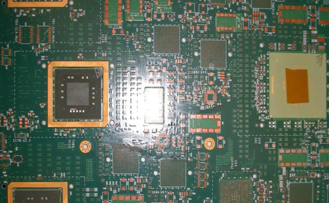
Advances in 3D Simulations of Chip/Package/PCB Co-Design
|
|
|
- Lindsay Flowers
- 5 years ago
- Views:
Transcription

1 Advances in 3D Simulations of Chip/Package/PCB Co-Design Richard Sjiariel, CST AG


2 Co-design environment Signal Integrity and timing Thermal analysis and stress Power Integrity and noise analysis EMC/EMI and radiation


3 Analysis across Chip/Package/PCB Nanometer scale Multi Gb PCB systems Need for co-design

4 Co-design Chip/interposer Board/Package Simplistic approach to CPB co-simulation may miss critical physics of the chip-package and package-board interactions. High-order electromagnetic interactions in the CPB system have a critical impact on the system integrity.
5 Co-design methodologies 1) Cascading approaches field based (continuity of E/H field and reference plane where propagating more is TEM) - PCB and Package Co/Design and Co/Optimization S-parameters based considering all pins (signal/pwr/gnd vias) 2) Simulation of the full system (Full 3D EM solvers or hybrid solvers)


6 S-Parameter Based Electric wall and ports at the interface Source: Zhaoqing Chen, General Co-Design Approach to Multi-Level Package Modeling based on Individual Single-Level Package Full-Wave S-Parameter Modeling Including Signal and Power/Ground Ports, ECTC 2012

7 Test Case (1/2) PCB + Package Package Signal vias PCB Signal vias PWR/GND vias PWR/GND vias Signal vias


8 Test Case (2/2) Package PCB The effect of the discrete port is de-embedded from the S-parameters of both PCB and package using c=-0.11pf
9 Results: Full Model vs. Cascaded Ins./return loss NEXT/FEXT (+) Very small difference between full model vs. cascaded model (-) Methodology difficult to use (prone to errors) when dealing with realistic models with many signal/power/gnd vias


10 PCB/Package Co-Design Pkg1: 2.5x2.5cm 21 layers Pkg2: 2.8x2.5cm, 21 layers


11 Geometry Details 1, 2 input-output 3, NEXT 4, FEXT 3 1 Multiple 3D geometries and RPDs: PTH BGA and bumps Micro vias..etc 4 2
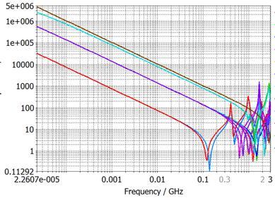
12 PCB vs Channel (PCB + Package) S11 full channel S11 PCB only S21 PCB only S21 full channel pkg1 PCB pkg2 Insertion loss S21-5 to 8dB difference in attenuation Return loss S11 large discrepancy in range 2-8GHz showing underestimation of impedance match for PCB model

13 Statistics Hardware(Nehalem) GPU Simulation Time/h Speed-up factor 1 node node cluster node cluster


14 Chip Modeling IBIS SPICE CPM/SPICE CAD EM modeling

15 Chip/Package/Board (CPB) Co-Design The anti-resonance peak occurs at the cross point of package inductance and chip capacitance. This is called chip-package anti-resonance. Source: R. Kobayashi et al, Effects of Critically Damped Total PDN Impedance in Chip-Package-Board Co-Design, IEEE EMC Conference, Pittsburgh 2012.

16 IBIS/SPICE Workflow Example DIE PKG Socket PCB Fixtures IBIS SPICE Signal Net Power Plane Pogo Pin Signal Trace Power Plane SMA Cable Scope


17 3D Model Victim Line Aggressor Lines 372x205mm large, 17 layers PCB Epsr=3.9, tgδ layers package with bond wires

18 Full System simulation PCB + package+ pogo pin Chip/ASIC
19 Comparison: Insertion Loss (Single Ended) Package + board + all nets = 3.16db Package + board + single net +-2.9db Package + board + all nets = 3.16db Package + board + all nets Package + board + single net Package only
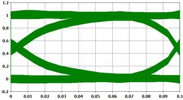
20 Transient Response Co-Simulation Port 17 represents an output result at PCB More realistic result helps to find the correct parameter for equalizer


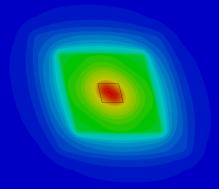
21 Surface Currents Surface current at 1GHz
 coupling Time Domain Field")
22 Strong coupling with neighbor nets Package/pogo pin to PCB (vertical) coupling Time Domain Field Monitor

23 SPICE/CPM A CPM (Chip Power Model) is a compact SPICE model of the full-chip power delivery network (PDN). It contains spatial and temporal current switching profiles, as well as parasitic of the non-linear on-chip devices +


24 CPM model validation Automatic assignment of current profiles/ports CST DS results SPICE results


25 SPICE/CPM Workflow Example PCB package 86x86mm 6 layer PCB epsr=3.57, tgδ=0.025 die
 PCB + package SPICE + Current")
26 CPB System Co-Simulation Drivers (IBIS) PCB + package SPICE + Current profiles
27 Current Profiles Currents feeding into package Switching current at chip

28 Current seems to be confined in island, but it progressively couples to the rest of the structure Field Monitor


29 Surface Current Distribution f=1ghz f=1ghz f=10ghz f=10ghz


30 EMC/EMI Analysis Farfield monitor probes at 3m
31 Summary Importance of chip/package/board (CPB) co-design is highlighted and its integration into various simulation workflows is discusses True transient co-simulation is a key feature for CPB co-design 3D packages with embedded chips 3D system integration 3D full wave simulation is only choice for accurate results
High Speed and High Power Connector Design
 High Speed and High Power Connector Design Taiwan User Conference 2014 Introduction High speed connector: Electrically small Using differential signaling Data rate >100Mbps High power connector: Static
Cadence Power Integrity Solutions For PCBs and IC Packages. May 2013
 Cadence Power Integrity Solutions For PCBs and IC Packages May 2013 Simultaneous Switching Noise (SSN) A Power Integrity Issue Design with decaps intentionally removed to demonstrate how poor PI performance
Advanced SI Analysis Layout Driven Assembly. Tom MacDonald RF/SI Applications Engineer II
 Advanced SI Analysis Layout Driven Assembly 1 Tom MacDonald RF/SI Applications Engineer II Abstract As the voracious appetite for technology continually grows, so too does the need for fast turn around
Integrating ADS into a High Speed Package Design Process
 Integrating ADS into a High Speed Package Design Process Page 1 Group/Presentation Title Agilent Restricted Month ##, 200X Agenda High Speed SERDES Package Design Requirements Performance Factor and Design
SSO Noise And Conducted EMI: Modeling, Analysis, And Design Solutions
 SSO Noise And Conducted EMI: Modeling, Analysis, And Design Solutions Patrice Joubert Doriol 1, Aurora Sanna 1, Akhilesh Chandra 2, Cristiano Forzan 1, and Davide Pandini 1 1 STMicroelectronics, Central
Stacked IC Analysis Modeling for Power Noise Impact
 Si2 Open3D Kick-off Meeting June 7, 2011 Stacked IC Analysis Modeling for Power Noise Impact Aveek Sarkar Vice President Product Engineering & Support Stacked IC Design Needs Implementation Electrical-,
New Technologies in CST STUDIO SUITE CST COMPUTER SIMULATION TECHNOLOGY
 New Technologies in CST STUDIO SUITE 2016 Outline Design Tools & Modeling Antenna Magus Filter Designer 2D/3D Modeling 3D EM Solver Technology Cable / Circuit / PCB Systems Multiphysics CST Design Tools
EM Analysis of High Frequency Printed Circuit Boards. Dr.-Ing. Volker Mühlhaus
 EM Analysis of High Frequency Printed Circuit Boards Dr.-Ing. Volker Mühlhaus volker@muehlhaus.com Agenda EM tools overview When to use EM analysis Application examples: Filters The importance of meshing
SSO Noise And Conducted EMI: Modeling, Analysis, And Design Solutions
 SSO Noise And Conducted EMI: Modeling, Analysis, And Design Solutions Patrice Joubert Doriol 1, Aurora Sanna 1, Akhilesh Chandra 2, Cristiano Forzan 1, and Davide Pandini 1 1 STMicroelectronics, Central
Impact of Embedded Capacitance on Test Socket and Test Board Performance Michael Giesler, 3M, Alexander Barr, 3M Yoshihisa Kawate,
 Impact of Embedded Capacitance on Test Socket and Test Board Performance Michael Giesler, 3M, msgiesler@mmm.com Alexander Barr, 3M Yoshihisa Kawate, Sumitomo-3M Yuichi Tsubaki, Sumitomo-3M Silicon Valley
Recent Via Modeling Methods for Multi-Vias in a Shared Anti-pad
 Recent Via Modeling Methods for Multi-Vias in a Shared Anti-pad Yao-Jiang Zhang, Jun Fan and James L. Drewniak Electromagnetic Compatibility (EMC) Laboratory, Missouri University of Science &Technology
Best practices for EMI filtering and IC bypass/decoupling applications
 X2Y Component Connection and PCB Layout Guidelines Best practices for EMI filtering and IC bypass/decoupling applications X2Y Attenuators, LLC 1 Common X2Y Circuit Uses EMI FILTERING Conducted and Radiated
Optimum Placement of Decoupling Capacitors on Packages and Printed Circuit Boards Under the Guidance of Electromagnetic Field Simulation
 Optimum Placement of Decoupling Capacitors on Packages and Printed Circuit Boards Under the Guidance of Electromagnetic Field Simulation Yuzhe Chen, Zhaoqing Chen and Jiayuan Fang Department of Electrical
An Innovative Simulation Workflow for Debugging High-Speed Digital Designs using Jitter Separation
 An Innovative Simulation Workflow for Debugging High-Speed Digital Designs using Jitter Separation C. Chastang, A. Amédéo V. Poisson, P. Grison, F. Demuynck C. Gautier, F. Costa Thales Communications &
EDA365. DesignCon Impact of Backplane Connector Pin Field on Trace Impedance and Vertical Field Crosstalk
 DesignCon 2007 Impact of Backplane Connector Pin Field on Trace Impedance and Vertical Field Crosstalk Ravi Kollipara, Rambus, Inc. ravik@rambus.com, (650) 947-5298 Ben Chia, Rambus, Inc. Dan Oh, Rambus,
Model Connection Protocol extensions for Mixed Signal SiP
 Model Connection Protocol extensions for Mixed Signal SiP Taranjit Kukal (kukal@cadence.com) Dr. Wenliang Dai (wldai@cadence.com) Brad Brim (bradb@sigrity.com) Presented by: Yukio Masuko Cadence Note:
A Proposal for Developing S2IBISv3
 A Proposal for Developing S2IBISv3 Paul Franzon Michael Steer Automated Design Tools for Integrated Mixed Signal Microsystems (NeoCAD) Outline Background DARPA Program NeoCad Program Objectives Program
Optimization of Modern Memory
 System Design, Verificationand and Optimization of Modern Memory Interfaces (DDR3) Santa Clara, Aug 23 rd 2011 Robert Myoung Sr. Application Engineer 1 Agenda Introduction ECAD Geometry Translation SI/PI
Agenda TDR Measurements Using Real World Products
 Agenda TDR Measurements Using Real World Products The Case for using both TDR and S-parameters Device Package Analysis - Measure Impedance -C-self Characterizing Device Evaluation Test board Measure Differential
Calibrating Achievable Design GSRC Annual Review June 9, 2002
 Calibrating Achievable Design GSRC Annual Review June 9, 2002 Wayne Dai, Andrew Kahng, Tsu-Jae King, Wojciech Maly,, Igor Markov, Herman Schmit, Dennis Sylvester DUSD(Labs) Calibrating Achievable Design
TABLE OF CONTENTS 1.0 PURPOSE INTRODUCTION ESD CHECKS THROUGHOUT IC DESIGN FLOW... 2
 TABLE OF CONTENTS 1.0 PURPOSE... 1 2.0 INTRODUCTION... 1 3.0 ESD CHECKS THROUGHOUT IC DESIGN FLOW... 2 3.1 PRODUCT DEFINITION PHASE... 3 3.2 CHIP ARCHITECTURE PHASE... 4 3.3 MODULE AND FULL IC DESIGN PHASE...
Future Directions in Computational Electromagnetics for Digital Applications
 Prof. Dr.-Ing. Future Directions in Computational Electromagnetics for Digital Applications Technische Universität Darmstadt Fachbereich Elektrotechnik und Informationstechnik Schloßgartenstr. 8, D64289
Allegro Sigrity SI Streamlining the creation of high-speed interconnect on digital PCBs and IC packages
 Streamlining the creation of high-speed interconnect on digital PCBs and IC packages The Cadence Allegro Sigrity signal integrity (SI) integrated high-speed design and analysis environment streamlines
Package on Board Simulation with 3-D Electromagnetic Simulation
 White Paper Package on Board Simulation with 3-D Electromagnetic Simulation For many years, designers have taken into account the effect of package parasitics in simulation, from using simple first-order
EMI/ESD Filters for Cellular Phones
 EMI/ESD Filters for Cellular Phones Cellular phones, as with all handheld and wireless devices are susceptible to the damaging effects of Electrostatic Discharge (ESD) transients. As much as 40 kilovolts
For functionality and CAD/EDA import filter, see technical specifications of the CST STUDIO SUITE
 CST MICROWAVE STUDIO Technical Specification 1 May 2015 Frontend Module For functionality and CAD/EDA import filter, see technical specifications of the CST STUDIO SUITE Transient Solver Module Fast and
Using Sonnet in a Cadence Virtuoso Design Flow
 Using Sonnet in a Cadence Virtuoso Design Flow Purpose of this document: This document describes the Sonnet plug-in integration for the Cadence Virtuoso design flow, for silicon accurate EM modelling of
Board Design Guidelines for PCI Express Architecture
 Board Design Guidelines for PCI Express Architecture Cliff Lee Staff Engineer Intel Corporation Member, PCI Express Electrical and Card WGs The facts, techniques and applications presented by the following
Apache s Power Noise Simulation Technologies
 Enabling Power Efficient i Designs Apache s Power Noise Simulation Technologies 1 Aveek Sarkar VP of Support Apache Design Inc, A wholly owned subsidiary of ANSYS Trends in Today s Electronic Designs Low-power
Use of Simulation Software in Pre-Qualification Tests
 Use of Simulation Software in Pre-Qualification Tests RF & Hyper Europe 2009 Villepinte Yannis Braux: Senior EM Engineer CST FRANCE 1 www.cst.com Use of Simulation Software in Pre-Qualification Tests 1.
Crosstalk Measurements for Signal Integrity Applications. Chris Scholz, Ph.D. VNA Product Manager R&S North America
 Crosstalk Measurements for Signal Integrity Applications Chris Scholz, Ph.D. VNA Product Manager R&S North America Outline ı A brief history of crosstalk ı Introduction to crosstalk Definition of crosstalk
Electrical optimization and simulation of your PCB design
 Electrical optimization and simulation of your PCB design Steve Gascoigne Senior Consultant at Mentor Graphics Zagreb, 10. lipnja 2015. Copyright CADCAM Group 2015 The Challenge of Validating a Design..
Chip/Package/Board Design Flow
 Chip/Package/Board Design Flow EM Simulation Advances in ADS 2011.10 1 EM Simulation Advances in ADS2011.10 Agilent EEsof Chip/Package/Board Design Flow 2 RF Chip/Package/Board Design Industry Trends Increasing
Practical Shielding, EMC/EMI, Noise Reduction, Earthing and Circuit Board Layout
 Practical Shielding, EMC/EMI, Noise Reduction, Earthing and Circuit Board Layout Contents 1 Introduction 1 1.1 Introduction 1 1.2 EMI vs EMC 3 1.3 Interference sources 3 1.4 Need for standards 5 1.5 EMC
Electromagnetic Compatibility ( EMC )
") Electromagnetic Compatibility ( EMC ) ESD Strategies in IC and System Design 8-1 Agenda ESD Design in IC Level ( ) Design Guide Lines CMOS Design Process Level Method Circuit Level Method Whole Chip Design
Electromagnetic Compatibility ( EMC ) ESD Strategies in IC and System Design 8-1 Agenda ESD Design in IC Level ( ) Design Guide Lines CMOS Design Process Level Method Circuit Level Method Whole Chip Design
ECE 5745 Complex Digital ASIC Design Topic 7: Packaging, Power Distribution, Clocking, and I/O
 ECE 5745 Complex Digital ASIC Design Topic 7: Packaging, Power Distribution, Clocking, and I/O Christopher Batten School of Electrical and Computer Engineering Cornell University http://www.csl.cornell.edu/courses/ece5745
ANSYS HFSS: Layout Driven Assembly in ANSYS Electronics Desktop
 Application Brief ANSYS HFSS: Layout Driven Assembly The ANSYS Electronics Desktop (AEDT) is an integrated environment with an easy-to-use interface that provides a streamlined workflow between ANSYS EM
*Note: Operation beyond this range is possible, but has not been characterized. PART. Maxim Integrated Products 1
 19-8; Rev ; 2/ EVALUATION KIT AVAILABLE 8MHz to MHz Variable-Gain General Description The MAX6 general-purpose, high-performance variable-gain amplifier (VGA) is designed to operate in the 8MHz to MHz
CHAPTER 2 NEAR-END CROSSTALK AND FAR-END CROSSTALK
 24 CHAPTER 2 NEAR-END CROSSTALK AND FAR-END CROSSTALK 2.1 INTRODUCTION The high speed digital signal propagates along the transmission lines in the form of transverse electromagnetic (TEM) waves at very
A Modular Platform for Accurate Multi- Gigabit Serial Channel Validation
 A Modular Platform for Accurate Multi- Gigabit Serial Channel Validation Presenter: Andrew Byers Ansoft Corporation High Performance Electronics: Technical Challenges Faster data rates in increasingly
Virtuoso System Design Platform Unified system-aware platform for IC and package design
 Unified system-aware platform for IC and package design The Cadence Virtuoso System Design Platform is a holistic, system-based solution that provides the functionality to drive simulation and LVS-clean
SFC ChipClamp ΤΜ Flip Chip TVS Diode with T-Filter PRELIMINARY Features
 Description The SFC2282-50 is a low pass T-filter with integrated TVS diodes. It is designed to provide bidirectional filtering of EMI/RFI signals and electrostatic discharge (ESD) protection in portable
A Proposed Set of Specific Standard EMC Problems To Help Engineers Evaluate EMC Modeling Tools
 A Proposed Set of Specific Standard EMC Problems To Help Engineers Evaluate EMC Modeling Tools Bruce Archambeault, Ph. D Satish Pratapneni, Ph.D. David C. Wittwer, Ph. D Lauren Zhang, Ph.D. Juan Chen,
Construction of an electrical model of a TQFP100 package with IC-EMC
 Construction of an electrical model of a TQFP100 package with IC-EMC A. Boyer INSA-GEI, 135 Av de Rangueil 31077 Toulouse France Contact : alexandre.boyer@insa-toulouse.fr web site : www.ic-emc.org Abstract:
Solving the challenges posed by Chip/Package/Board Co-Design
 Solving the challenges posed by Chip/Package/Board Co-Design Identify and locate sources of unwanted coupling Simulation link to EM: Critical Interconnect, Vias, Discontinuities, Embedded Passives, etc
Chip-Package-Board Co-Design / Co-Verification Technology for DDR3 1.6G in Consumer Products
 Chip-Package-Board Co-Design / Co-Verification Technology for DDR3 1.6G in Consumer Products Ji Zheng Director, Chip Package System Apache Design Solutions 2011 ASP-DAC Designer s Forum January 27, 2011
AN-1055 APPLICATION NOTE
 AN-155 APPLICATION NOTE One Technology Way P.O. Box 916 Norwood, MA 262-916, U.S.A. Tel: 781.329.47 Fax: 781.461.3113 www.analog.com EMC Protection of the AD7746 by Holger Grothe and Mary McCarthy INTRODUCTION
IBIS PDN Feature Studies
 IBIS PDN Feature Studies Randy Wolff Micron Technology Lance Wang IO Methodology DAC IBIS Summit San Diego, CA, USA based on 2011 European IBIS Summit presentation and updates 2010 Micron Technology, Inc.
Application Note AN105 A1. PCB Design and Layout Considerations for Adesto Memory Devices. March 8, 2018
 Application Note AN105 A1 PCB Design and Layout Considerations for Adesto Memory Devices March 8, 2018 Adesto Technologies 2018 3600 Peterson Way Santa Clara CA. 95054 Phone 408 400 0578 www.adestotech.com
Design Guideline for TC1782 Microcontroller Board Layout
 TC1782 AP32145 Application Note V1.4 2012-02 Microcontrollers Edition 2012-02 Published by Infineon Technologies AG 81726 Munich, Germany 2012 Infineon Technologies AG All Rights Reserved. LEGAL DISCLAIMER
EXAMINING THE IMPACT OF SPLIT PLANES ON SIGNAL AND POWER INTEGRITY
 EXAMINING THE IMPACT OF SPLIT PLANES ON SIGNAL AND POWER INTEGRITY Jason R. Miller, Gustavo J. Blando, Roger Dame, K. Barry A. Williams and Istvan Novak Sun Microsystems, Burlington, MA 1 AGENDA Introduction
Physical Aspects of Packages for 100GEL & PKG ad-hoc Physical Aspects Summary
 Physical Aspects of Packages for 100GEL & PKG ad-hoc Physical Aspects Summary Liav Ben Artsi, Marvell Israel Ltd. September 2018 Suggested PKG Model Cases Length Ball Side Discontinuity Xtalk (Suggest
PI2EQX6874ZFE 4-lane SAS/SATA ReDriver Application Information
 Contents General Introduction How to use pin strap and I2C control External Components Requirement Layout Design Guide Power Supply Bypassing Power Supply Sequencing Equalization Setting Output Swing Setting
Area Array Probe Card Interposer. Raphael Robertazzi IBM Research 6/4/01. 6/4/01 IBM RESEARCH Page [1]
![Area Array Probe Card Interposer. Raphael Robertazzi IBM Research 6/4/01. 6/4/01 IBM RESEARCH Page [1]](/thumbs/78/78371092.jpg "Area Array Probe Card Interposer. Raphael Robertazzi IBM Research 6/4/01. 6/4/01 IBM RESEARCH Page [1]") Area Array Probe Card Interposer Raphael Robertazzi IBM Research 6/4/01 6/4/01 IBM RESEARCH Page [1] Motivation: Outline Probe Cards for Testing Complex ICs in the Developmental Stage. Hand Wired Space
Area Array Probe Card Interposer Raphael Robertazzi IBM Research 6/4/01 6/4/01 IBM RESEARCH Page [1] Motivation: Outline Probe Cards for Testing Complex ICs in the Developmental Stage. Hand Wired Space
HFSS 14 Update for SI and RF Applications Markus Kopp Product Manager, Electronics ANSYS, Inc.
 HFSS 14 Update for SI and RF Applications Markus Kopp Product Manager, Electronics ANSYS, Inc. 1 ANSYS, Inc. September 21, Advanced Solvers: Finite Arrays with DDM 2 ANSYS, Inc. September 21, Finite Arrays
Lecture 2: Introduction
 Lecture 2: Introduction v2015.0 Release ANSYS HFSS for Antenna Design 1 2015 ANSYS, Inc. Multiple Advanced Techniques Allow HFSS to Excel at a Wide Variety of Applications Platform Integration and RCS
Over 5,000 products High Performance Adapters and Sockets Many Custom Designs Engineering Electrical and Mechanical ISO9001:2008 Registration
 Overview Company Overview Over 5,000 products High Performance Adapters and Sockets Many Custom Designs Engineering Electrical and Mechanical ISO9001:2008 Registration Adapter Technology Overview Pluggable
Additional Slides for Lecture 17. EE 271 Lecture 17
 Additional Slides for Lecture 17 Advantages/Disadvantages of Wire Bonding Pros Cost: cheapest packages use wire bonding Allows ready access to front side of die for probing Cons Relatively high inductance
DesignCon 2005 Track 5: Chip and Board Interconnect Design (5-TA2)
") DesignCon 2005 Track 5: Chip and Board Interconnect Design (5-TA2) Connector-Less Probing: Electrical and Mechanical Advantages Authors/Presenters: Brock LaMeres, Agilent Technologies Brent Holcombe, Agilent
DesignCon 2005 Track 5: Chip and Board Interconnect Design (5-TA2) Connector-Less Probing: Electrical and Mechanical Advantages Authors/Presenters: Brock LaMeres, Agilent Technologies Brent Holcombe, Agilent
Advances in Measurement Based Transient Simulation
 Time Domain Simulation in ADS, Slide - 1 Advances in Measurement Based Transient Simulation Presented by GigaTest Labs Gary Otonari and Orlando Bell March, 2008 1 Time Domain Simulation in ADS, Slide -
PI2EQX6804-ANJE Four-lane SAS/SATA ReDriver Application Information May 13, 2011
 Contents General Introduction How to use pin strap and I2C control External Components Requirement Layout Design Guide Power Supply Bypassing Power Supply Sequencing Equalization Setting Output Swing Setting
SOI REQUIRES BETTER THAN IR-DROP. F. Clément, CTO
 SOI REQUIRES BETTER THAN IR-DROP F. Clément, CTO Content IR Drop Vs. System-level Interferences CWS Expertise Accuracy and Performance Silicon Validation Conclusion Copyright CWS 2004-2016 2 Sensitive
Electromagnetics. R14 Update. Greg Pitner ANSYS, Inc. February 24, 2012
 Electromagnetics R14 Update Greg Pitner 1 HFSS Version 14 2 HFSS Overview Advanced Integrated Solver Technologies Finite Arrays with Domain Decomposition Hybrid solving: FEBI, IE Regions Physical Optics
Aspects of RF Simulation and Analysis Software Methods. David Carpenter. Remcom. B = t. D t. Remcom (Europe)
") Remcom (Europe) Central Boulevard Blythe Valley Park Solihull West Midlands England, B90 8AG www.remcom.com +44 870 351 7640 +44 870 351 7641 (fax) Aspects of RF Simulation and Analysis Software Methods
Remcom (Europe) Central Boulevard Blythe Valley Park Solihull West Midlands England, B90 8AG www.remcom.com +44 870 351 7640 +44 870 351 7641 (fax) Aspects of RF Simulation and Analysis Software Methods
Case study of IBIS V4.1 by JEITA EDA-WG
 Case study of IBIS V4.1 by JEITA EDA-WG June 8, 2004 IBIS SUMMIT in San Diego, California JEITA EDA-WG A. Itoh,, T. Watanabe, N. Matsui JEITA ; Japan Electronics and Information Technology Industries Association
Adapter Technologies
 Adapter Technologies Toll Free: (800) 404-0204 U.S. Only Tel: (952) 229-8200 Fax: (952) 229-8201 email: info@ironwoodelectronics.com Introduction Company Overview Over 5,000 products High Performance Adapters
CBC performance with switched capacitor DC-DC converter. Mark Raymond, Tracker Upgrade Power Working Group, February 2012.
 CBC performance with switched capacitor DC-DC converter Mark Raymond, Tracker Upgrade Power Working Group, February 212. 1 CBC power features 2 powering features included on CBC prototype pads for test
Wie entsteht ein EMV-Modell für eine integrierte Schaltung?
 Wie entsteht ein EMV-Modell für eine integrierte Schaltung? P. Schneider Overview Motivation Introduction Signal- and Power Integrity Simulation Tools Input Data Preparation gds2def & Power Annotation
TECHNOLOGY SYSTEM-LEVEL SIMULATION. S.P. Levitan and D.M. Chiarulli University of Pittsburgh, Pittsburgh, PA USA
 MULTI-LEVEL LEVEL MIXED- TECHNOLOGY SYSTEM-LEVEL SIMULATION S.P. Levitan and D.M. Chiarulli University of Pittsburgh, Pittsburgh, PA 15260 USA Collaborators and Support Jose A. Martinez, Mark Kahrs, Jason
GT Micro D High Speed Characterization Report For Differential Data Applications. Micro-D High Speed Characterization Report
 GT-14-19 Micro D For Differential Data Applications GMR7580-9S1BXX PCB Mount MWDM2L-9P-XXX-XX Cable Mount Revision History Rev Date Approved Description A 4/10/2014 C. Parsons/D. Armani Initial Release
RiseUp RU8-DP-DV Series 19mm Stack Height Final Inch Designs in PCI Express Applications. Revision Date: March 18, 2005
 RiseUp RU8-DP-DV Series 19mm Stack Height Final Inch Designs in PCI Express Applications Revision Date: March 18, 2005 Copyrights and Trademarks Copyright 2005 Samtec, Inc. Developed in conjunction with
A Practical Approach to Preventing Simultaneous Switching Noise and Ground Bounce Problems in IO Rings
 A Practical Approach to Preventing Simultaneous Switching Noise and Ground Bounce Problems in IO Rings Dr. Osman Ersed Akcasu, Jerry Tallinger, Kerem Akcasu OEA International, Inc. 155 East Main Avenue,
Receiver Modeling for Static Functional Crosstalk Analysis
 Receiver Modeling for Static Functional Crosstalk Analysis Mini Nanua 1 and David Blaauw 2 1 SunMicroSystem Inc., Austin, Tx, USA Mini.Nanua@sun.com 2 University of Michigan, Ann Arbor, Mi, USA Blaauw@eecs.umich.edu
BGA Crosstalk. Thank you for inviting me to speak at this tech online forum.
 BGA Crosstalk by Dr. Howard Johnson Xilinx Virtex-4 FPGA and Altera Stratix II FPGA Details, measured lab results, and theory of crosstalk involving hundreds of outputs switching simultaneously in a high-speed
Toshiba Case Study RF Module Shrink (TransferJet TM )
") Toshiba Case Study RF Module Shrink (TransferJet TM ) These slides are an abridgement of two presentations given by Toshiba at the Zuken Innovation World (ZIW) conference held in Japan in 2012 and 2013.
Toshiba Case Study RF Module Shrink (TransferJet TM ) These slides are an abridgement of two presentations given by Toshiba at the Zuken Innovation World (ZIW) conference held in Japan in 2012 and 2013.
An Adaptable Test Socket Concept that Meets Both the Test and Burn-In Needs of 21st Century Array Packages
 An Adaptable Test Socket Concept that Meets Both the Test and Burn-In Needs of 21st Century Array Packages Alexander Barr, 3M, awbarr@mmm.com Akihiko Furuta, Sumitomo 3M, Masahiko Kobayashi, Sumitomo 3M,
Advanced Surface Based MoM Techniques for Packaging and Interconnect Analysis
 Electrical Interconnect and Packaging Advanced Surface Based MoM Techniques for Packaging and Interconnect Analysis Jason Morsey Barry Rubin, Lijun Jiang, Lon Eisenberg, Alina Deutsch Introduction Fast
Interconnect Impedance Measurements, Signal Integrity Modeling, Model Validation, and Failure Analysis. IConnect TDR Software.
 Rev. 8/27/21 Interconnect Impedance Measurements, Signal Integrity Modeling, Model Validation, and Failure Analysis IConnect TDR Software TDA Systems, Inc. www.tdasystems.com Outline TDR Impedance Measurements
Modern Memory Interfaces (DDR3) Design with ANSYS Virtual Prototype approach
 Design with ANSYS Virtual Prototype approach") Modern Memory Interfaces (DDR3) Design with ANSYS Virtual Prototype approach 1 ANSYS, Inc. Proprietary 2012 ANSYS, Inc. November 14, 2012 1-1 Agenda DDR Design Challenges How does simulation solve these
Modern Memory Interfaces (DDR3) Design with ANSYS Virtual Prototype approach 1 ANSYS, Inc. Proprietary 2012 ANSYS, Inc. November 14, 2012 1-1 Agenda DDR Design Challenges How does simulation solve these
Signal Integrity Analysis and Simulation on 3D-ICs
 Signal Integrity Analysis and Simulation on 3D-ICs Nikolaos Gkolemis Department of Electrical Engineering University of California, Los Angeles ngkolemis@ucla.edu Yubo Wang Department of Electrical Engineering
ANSYS, Inc. March 3, 2016 PCB 板极电热耦合分析及对电子设备热设计的影响
 1 2015 ANSYS, Inc. March 3, 2016 PCB 板极电热耦合分析及对电子设备热设计的影响 Printed Circuit Board Reliability Real world operating conditions = Multiphysics environment Electrical Reliability Power and Signal Integrity
Q Pairs QTE/QSE-DP Final Inch Designs In PCI Express Applications 16 mm Stack Height
 Application Note Q Pairs QTE/QSE-DP Final Inch Designs In PCI Express Applications 16 mm Stack Height Copyrights and Trademarks Copyright 2004 Samtec, Inc. Developed in conjunction with Teraspeed Consulting
Low-Capacitance, 2/3/4/6-Channel, ±15kV ESD Protection Arrays for High-Speed Data Interfaces
 9-739; Rev 5; 6/ General Description The are low-capacitance ±5kV ESD-protection diode arrays designed to protect sensitive electronics attached to communication lines. Each channel consists of a pair
Interconnect Challenges in a Many Core Compute Environment. Jerry Bautista, PhD Gen Mgr, New Business Initiatives Intel, Tech and Manuf Grp
 Interconnect Challenges in a Many Core Compute Environment Jerry Bautista, PhD Gen Mgr, New Business Initiatives Intel, Tech and Manuf Grp Agenda Microprocessor general trends Implications Tradeoffs Summary
Simulation Strategies for Massively Parallel Supercomputer Design
 Simulation Strategies for Massively Parallel Supercomputer Design Authored by: Ansoft Corporation Special Thanks to: Cray Presentation #2 Ansoft 2003 / Global Seminars: Delivering Performance Introduction
Signal Integrity Comparisons Between Stratix II and Virtex-4 FPGAs
 White Paper Introduction Signal Integrity Comparisons Between Stratix II and Virtex-4 FPGAs Signal integrity has become a critical issue in the design of high-speed systems. Poor signal integrity can mean
Application Suggestions for X2Y Technology
 Application Suggestions for X2Y Technology The following slides show applications that would benefit from balanced, low inductance X2Y devices. X2Y devices can offer a significant performance improvement
SIMULATION OF AN IMPLANTED PIFA FOR A CARDIAC PACEMAKER WITH EFIELD FDTD AND HYBRID FDTD-FEM
 1 SIMULATION OF AN IMPLANTED PIFA FOR A CARDIAC PACEMAKER WITH EFIELD FDTD AND HYBRID FDTD- Introduction Medical Implanted Communication Service (MICS) has received a lot of attention recently. The MICS
Simulation Advances for RF, Microwave and Antenna Applications
 Simulation Advances for RF, Microwave and Antenna Applications Bill McGinn Application Engineer 1 Overview Advanced Integrated Solver Technologies Finite Arrays with Domain Decomposition Hybrid solving:
Wafer Level Packaging The Promise Evolves Dr. Thomas Di Stefano Centipede Systems, Inc. IWLPC 2008
 Wafer Level Packaging The Promise Evolves Dr. Thomas Di Stefano Centipede Systems, Inc. IWLPC 2008 / DEVICE 1.E+03 1.E+02 1.E+01 1.E+00 1.E-01 1.E-02 1.E-03 1.E-04 1.E-05 1.E-06 1.E-07 Productivity Gains
CitrusCom CS0806U. Features. Applications. Mechanical Characteristics. Description. Circuit Diagram. Pin Configuration
 Features Transient protection for high-speed data lines IEC 1000--2 (ESD) ±1kV (Air) ±8kV (Contact) IEC 1000-- (EFT) 0A (/0 ns) Cable Discharge Event (CDE) Small package (2.9mm 2.8mm 1.mm) Protects four
HFSS 14 Update for SI and RF Applications. Presenter: Senior Application Engineer Jeff Tharp, Ph.D.
 HFSS 14 Update for SI and RF Applications Presenter: Senior Application Engineer Jeff Tharp, Ph.D. 1 Overview Advanced Integrated Solver Technologies Finite Arrays with Domain Decomposition Hybrid solving
RClamp TM 0504M RailClamp Low Capacitance TVS Diode Array PRELIMINARY Features
 Description RailClamps are surge rated diode arrays designed to protect high speed data interfaces. The RClamp series has been specifically designed to protect sensitive components which are connected
Session S0069: GPU Computing Advances in 3D Electromagnetic Simulation
 Session S0069: GPU Computing Advances in 3D Electromagnetic Simulation Andreas Buhr, Alexander Langwost, Fabrizio Zanella CST (Computer Simulation Technology) Abstract Computer Simulation Technology (CST)
Characterize and Debug Crosstalk Issues with Keysight Crosstalk Analysis App
 Chong Min-Jie Characterize and Debug Crosstalk Issues with Crosstalk Analysis App Page Characterize and Debug Crosstalk Issues with Crosstalk Analysis App Min-Jie Chong HPS Product Manager & Planner Oscilloscope
AOZ8882. Ultra-Low Capacitance TVS Diode Array. General Description. Features. Applications. Typical Application
 Ultra-Low Capacitance TS Diode Array General Description The AOZ8882 is a transient voltage suppressor array designed to protect high speed data lines such as HDMI, MDDI, USB, SATA, and Gigabit Ethernet
Package level Interconnect Options
 Package level Interconnect Options J.Balachandran,S.Brebels,G.Carchon, W.De Raedt, B.Nauwelaers,E.Beyne imec 2005 SLIP 2005 April 2 3 Sanfrancisco,USA Challenges in Nanometer Era Integration capacity F
TETRIS 1000 / High Impedance Active Probe Order-No: Features:
 Features: High Impedance Active Probe Order-No: 881-000-000 881-500-000 High Input Impedance Interchangeable Spring Tips Contacts adjacent Pins in 2.54 mm Pitch Useable with any 50 Ω Measuring Instrument
SAS-2 Internal Channel Modeling (05-276r0) Barry Olawsky Hewlett Packard r0 SAS-2 Channel Modeling 1
 Barry Olawsky Hewlett Packard r0 SAS-2 Channel Modeling 1") SAS-2 Internal Channel Modeling (05-276r0) Barry Olawsky Hewlett Packard 05-276r0 SAS-2 Channel Modeling 1 Project Goals Provide industry with data to better understand customer (hp and other OEMs) applications.
SAS-2 Internal Channel Modeling (05-276r0) Barry Olawsky Hewlett Packard 05-276r0 SAS-2 Channel Modeling 1 Project Goals Provide industry with data to better understand customer (hp and other OEMs) applications.
BGA SSD with EMI Shielding
 BGA SSD with EMI Shielding Jong-ok Chun Senior Managing Director Sun System Co.,Ltd www.sunsystem.kr rfjob@sunsysm.com, OCT-2017 Trend of SSD Form-Factor Form Factor - 2.5 Inch - Slim SATA 100x70mm 54x39mm