HFSS Solver-On-Demand for Package and PCB Characterization Using Cadence Greg Pitner
|
|
|
- Lisa McCarthy
- 6 years ago
- Views:
Transcription

1 HFSS Solver-On-Demand for Package and PCB Characterization Using Cadence Greg Pitner 1 ANSYS, Inc. September 14,
2 Problem Statement Usually SI engineers extract only the package or the pcb due to the trade-offs between capacity and simulation time For high speed channels, it is important to combine the package and pcb to capture the transitions in 3D Merging multi-layer package and pcb in 3D can be cumbersome 2 ANSYS, Inc. September 14,
3 Agenda Introduce HFSS in Cadence a HFSS Solver on Demand Technology Demonstrate ease of use of HFSS in Cadence for high speed I/O analysis using Xilinx Virtex6 package and pcb Exhibit the macro modeling ability within Designer through Network Data Explorer Demonstrate the new IBIS AMI importer which streamlines usage of IBIS AMI driver/receiver models Evaluate high speed channel performance with IBIS AMI driver/receiver models through eye diagrams 3 ANSYS, Inc. September 14,


4 HFSS in Cadence Enables More Robust 3D Investigation Today, we will show the advances that we have made in our Solver on Demand capabilities which enable The solving of larger 3D models to determine optimal performance The ability to add and solve manufacturing variations to the 3D model + = 4 ANSYS, Inc. September 14,
5 HFSS in Cadence Automation and Ease of Use Select nets of interest Signal, Power and Ground Draw extents to export selected portions of package or pcb Create ports on signal nets Specify HFSS solution setup Specify HFSS airbox extents 5 ANSYS, Inc. September 14,


6 HFSS in Cadence Package - Select Nets and Determine Extents 6 ANSYS, Inc. September 14,


7 HFSS in Cadence Package - Automatic Port Creation 7 ANSYS, Inc. September 14,
8 HFSS in Cadence Package - Airbox Extents and HFSS Solution Setup 8 ANSYS, Inc. September 14,

9 Package Model in Designer 2D Layout View Stackup Editor 9 ANSYS, Inc. September 14,


10 HFSS in Cadence Board - Select Signals and Draw Extents 10 ANSYS, Inc. September 14,

11 HFSS in Cadence Board - HFSS Solve Settings 11 ANSYS, Inc. September 14,

12 Board Model in Designer 2D Layout View Stackup Editor 12 ANSYS, Inc. September 14,


13 Create PCB Ports in Designer Select Trace Edges in Layout Automatically creates coupled waveport 13 ANSYS, Inc. September 14,


14 Merge Package on to PCB Package placement layer and position can be specified in the Footprint Package stackup is independent of the PCB Package layout is now a sub-circuit of the board cutout 14 ANSYS, Inc. September 14,

15 Merged Package and PCB Cutouts 2D Layout View 3D Layout View 15 ANSYS, Inc. September 14,
 17 ANSYS, Inc.")
16 Analyze Model from Designer (HFSS Solver-on-Demand) 17 ANSYS, Inc. September 14,

17 Export to 3D HFSS Model from Designer 18 ANSYS, Inc. September 14,

18 Differential Insertion and Return Loss Insertion Loss Return Loss 19 ANSYS, Inc. September 14,
19 Agenda Introduce HFSS in Cadence a HFSS Solver on Demand Technology Demonstrate ease of use of HFSS in Cadence for high speed I/O analysis using Xilinx Virtex6 package and pcb Exhibit the macro modeling ability within Designer through Network Data Explorer Demonstrate the new IBIS AMI importer which streamlines usage of IBIS AMI driver/receiver models Evaluate high speed channel performance with IBIS AMI driver/receiver models through eye diagrams 20 ANSYS, Inc. September 14,


20 Macro-modeling Functionality New functionality for the SI market HFSS Q3D Network Data Explorer State-space fitting Passivity enforcement Passivity checker S-parameter visualization S-matrix reduction Macro-model generation Circuit Simulation Designer Simplorer Other SIwave Designer Measured Data State-space Simplorer Spectre HSPICE PSPICE 21 ANSYS, Inc. September 14,


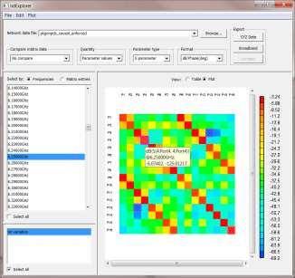
21 Network Data Explorer 22 ANSYS, Inc. September 14,

 23 ANSYS,")
22 Network Data Explorer The S-Parameter data can be converted to a macro model for use with circuit simulation in multiple formats: New! Advanced features Default (fast but memory intensive) Use perturbation when s-parameter model has many ports (>10) 23 ANSYS, Inc. September 14,
23 IBIS AMI AMI stands for Algorithmic Modeling Interface It allows users to specify their own transmitter and receiver models as C- interface compiled libraries Designer supports Matlab as well as compiled DLLs faster signal processing algorithms intellectual property protection Mainly used in convolution (fast) transient engines for channel simulation Designed to be used with fixed time step data Introduced in IBIS 5.0 specs IBIS stand for I/O Buffer Information Specification ; high-level buffer specification for circuit modeling In these specs the library is specified inside the IBIS wrapper and the interface is called IBIS- AMI In fact, AMI concept is independent of IBIS 24 ANSYS, Inc. September 14,


24 New AMI Import Process Import from.ibs file or specific.ami file directly 25 ANSYS, Inc. September 14,

25 New AMI Import Process 26 ANSYS, Inc. September 14, Automatically fill out fields for.dll and.so models Test button runs IBIS committee parser and reports pass/fail Advanced option used to set up models with non-standard behavior


26 I obe I urce AMI Source ID=26 R149 Port3 Port11 R150 Port4 Port12 R Port5 Port13 R R Port6 Port14 R Imported R Component 50 Port7 Port15 R159 Tx R Port8 Port16 R155 R156 R Rx ID=32 R ID= ANSYS, Inc. September 14, AMI model parameters can be sweep able component parameters upon import

27 AMI Probe AMI Source Schematic and Setup for AMI Analysis ID=26 R149 R150 R15150 R15250 R15350 R Port1 Port2 Port3 Port4 Port5 Port6 Port7 Port8 Port9 Port10 Port11 Port12 Port13 Port14 Port15 Port16 R155 R156 R R R R R6 ID=32 R Pkg on PCB model from HFSS Solver on Demand 15 inches long stripline differential pair from Designer library Makes use of GPU card 29 ANSYS, Inc. September 14,

28 Eye Opening Before Receiver 30 ANSYS, Inc. September 14,

29 Eye Opening After Receiver DFE 31 ANSYS, Inc. September 14,
30 Conclusions HFSS in Cadence enables SI engineers to setup and solve package and pcb models in 3D using HFSS Designer provides a complete framework to Import ready to solve models from third party layout Enables HFSS Solver on Demand to solve HFSS models Check for passivity and causality to determine quality of S parameters and W elements Enforce passivity and causality on S parameters and W elements Greatly simplify the reading and execution of AMI models for transmitter and receivers through the new AMI importer Validate channel performance with statistical eye diagrams and various eye measurements HFSS in Cadence (a Solver on Demand feature) greatly enhances productivity of an SI engineer 32 ANSYS, Inc. September 14,
HFSS Solver On Demand for Package and PCB Characterization Using Cadence. Greg Pitner
 HFSS Solver On Demand for Package and PCB Characterization Using Cadence Greg Pitner 1 Problem Statement Usually SI engineers extract only the package or the pcb due to the trade offs between capacity
Electromagnetics. R14 Update. Greg Pitner ANSYS, Inc. February 24, 2012
 Electromagnetics R14 Update Greg Pitner 1 HFSS Version 14 2 HFSS Overview Advanced Integrated Solver Technologies Finite Arrays with Domain Decomposition Hybrid solving: FEBI, IE Regions Physical Optics
Advanced SI Analysis Layout Driven Assembly. Tom MacDonald RF/SI Applications Engineer II
 Advanced SI Analysis Layout Driven Assembly 1 Tom MacDonald RF/SI Applications Engineer II Abstract As the voracious appetite for technology continually grows, so too does the need for fast turn around
HFSS 14 Update for SI and RF Applications Markus Kopp Product Manager, Electronics ANSYS, Inc.
 HFSS 14 Update for SI and RF Applications Markus Kopp Product Manager, Electronics ANSYS, Inc. 1 ANSYS, Inc. September 21, Advanced Solvers: Finite Arrays with DDM 2 ANSYS, Inc. September 21, Finite Arrays
Package on Board Simulation with 3-D Electromagnetic Simulation
 White Paper Package on Board Simulation with 3-D Electromagnetic Simulation For many years, designers have taken into account the effect of package parasitics in simulation, from using simple first-order
Optimization of Modern Memory
 System Design, Verificationand and Optimization of Modern Memory Interfaces (DDR3) Santa Clara, Aug 23 rd 2011 Robert Myoung Sr. Application Engineer 1 Agenda Introduction ECAD Geometry Translation SI/PI
Solving the challenges posed by Chip/Package/Board Co-Design
 Solving the challenges posed by Chip/Package/Board Co-Design Identify and locate sources of unwanted coupling Simulation link to EM: Critical Interconnect, Vias, Discontinuities, Embedded Passives, etc
Enabling SI Productivity Part 2. Venkatesh Seetharam Aaron Edwards
 Enabling SI Productivity Part 2 Venkatesh Seetharam Aaron Edwards 1 Problem Statement SI engineers use simulation software to squeeze the most performance out of their design. They will tend to focus on
Layer Stackup Wizard: Intuitive Pre-Layout Design
 Application Brief Layer Stackup Wizard: Intuitive Pre-Layout Design INTRODUCTION This Application Brief describes the Layer Stackup Wizard, a powerful utility within ANSYS SIwave for pre-layout stackup
ANSYS HFSS: Layout Driven Assembly in ANSYS Electronics Desktop
 Application Brief ANSYS HFSS: Layout Driven Assembly The ANSYS Electronics Desktop (AEDT) is an integrated environment with an easy-to-use interface that provides a streamlined workflow between ANSYS EM
ANSYS, Inc. March 3, 2016 PCB 板极电热耦合分析及对电子设备热设计的影响
 1 2015 ANSYS, Inc. March 3, 2016 PCB 板极电热耦合分析及对电子设备热设计的影响 Printed Circuit Board Reliability Real world operating conditions = Multiphysics environment Electrical Reliability Power and Signal Integrity
Allegro Sigrity SI Streamlining the creation of high-speed interconnect on digital PCBs and IC packages
 Streamlining the creation of high-speed interconnect on digital PCBs and IC packages The Cadence Allegro Sigrity signal integrity (SI) integrated high-speed design and analysis environment streamlines
Modern Memory Interfaces (DDR3) Design with ANSYS Virtual Prototype approach
 Design with ANSYS Virtual Prototype approach") Modern Memory Interfaces (DDR3) Design with ANSYS Virtual Prototype approach 1 ANSYS, Inc. Proprietary 2012 ANSYS, Inc. November 14, 2012 1-1 Agenda DDR Design Challenges How does simulation solve these
Modern Memory Interfaces (DDR3) Design with ANSYS Virtual Prototype approach 1 ANSYS, Inc. Proprietary 2012 ANSYS, Inc. November 14, 2012 1-1 Agenda DDR Design Challenges How does simulation solve these
A Modular Platform for Accurate Multi- Gigabit Serial Channel Validation
 A Modular Platform for Accurate Multi- Gigabit Serial Channel Validation Presenter: Andrew Byers Ansoft Corporation High Performance Electronics: Technical Challenges Faster data rates in increasingly
Board Design Guidelines for PCI Express Architecture
 Board Design Guidelines for PCI Express Architecture Cliff Lee Staff Engineer Intel Corporation Member, PCI Express Electrical and Card WGs The facts, techniques and applications presented by the following
Realize Your Product Promise. DesignerRF
 Realize Your Product Promise DesignerRF Four-element antenna array showing current distribution and far-field gain, created in DesignerRF using layout editor and solved via HFSS with Solver on Demand technology
designs with signals operating in the multi-gigahertz (MGH) frequency range. It
 frequency range. It") DATASHEET ALLEGRO PCB SI GXL Cadence Allegro PCB SI GXL provides a virtual prototyping environment for designs with signals operating in the multi-gigahertz (MGH) frequency range. It offers a completely
DATASHEET ALLEGRO PCB SI GXL Cadence Allegro PCB SI GXL provides a virtual prototyping environment for designs with signals operating in the multi-gigahertz (MGH) frequency range. It offers a completely
Simulation and Modeling for Signal Integrity and EMC
 Simulation and Modeling for Signal Integrity and EMC Lynne Green Sr. Member of Consulting Staff Cadence Design Systems, Inc. 320 120th Ave NE Bellevue, WA 98005 USA (425) 990-1288 http://www.cadence.com
ALLEGRO PCB SI 630 DATASHEET VIRTUAL PROTOTYPING ENVIRONMENT FOR DESIGNS WITH MULTI-GIGAHERTZ SIGNALS THE ALLEGRO SYSTEM INTERCONNECT DESIGN PLATFORM
 DATASHEET ALLEGRO PCB SI 630 VIRTUAL PROTOTYPING ENVIRONMENT FOR DESIGNS WITH MULTI-GIGAHERTZ SIGNALS Cadence Allegro PCB SI 630 a key PCB Signal Integrity tool within the Allegro system interconnect design
SPISim1. SPISim Modeling Suite. IBIS, IBIS-AMI model generation and general modeling
 SPISim1 SPISim Modeling Suite IBIS, IBIS-AMI model generation and general modeling SPISim EDA expertise in Signal, Power Integrity and Simulation EDA focusing on SI and PI: SPISim is an EDA company specialized
Using IBIS-AMI in the Modeling of Advanced SerDes Equalization for Serial Link Simulation
 Using IBIS-AMI in the Modeling of Advanced SerDes Equalization for Serial Link Simulation CDNLive Boston August 2013 Mark Marlett and Mahesh Tirupattur, Analog Bits Ken Willis and Kumar Keshavan, Cadence
AXIEM EM Simulation/Verification of a Cadence Allegro PCB
 Application Example AXIEM EM Simulation/Verification of a Cadence Allegro PCB Overview This application example outlines the electromagnetic (EM) simulation and verification flow that exists between Cadence
OrCAD for Education Program
 OrCAD for Education Program In partnership with Cadence Design Systems (the world s largest EDA software vendor), ECADtools administers the OrCAD for Education Program, which provides universities, electronics
Workshop 3-1: Coax-Microstrip Transition
 Workshop 3-1: Coax-Microstrip Transition 2015.0 Release Introduction to ANSYS HFSS 1 2015 ANSYS, Inc. Example Coax to Microstrip Transition Analysis of a Microstrip Transmission Line with SMA Edge Connector
Creating Xnets for Resistor Packs in Allegro PCB Editor. Product Version SPB16.6 April 2, 2014
 Creating Xnets for Resistor Packs in Allegro PCB Editor Product Version SPB16.6 April 2, 2014 Copyright Statement 2014 Cadence Design Systems, Inc. All rights reserved worldwide. Cadence and the Cadence
Integrating ADS into a High Speed Package Design Process
 Integrating ADS into a High Speed Package Design Process Page 1 Group/Presentation Title Agilent Restricted Month ##, 200X Agenda High Speed SERDES Package Design Requirements Performance Factor and Design
Chip/Package/Board Interface Pathway Design and Optimization. Tom Whipple Product Engineering Architect November 2015
 Chip/Package/Board Interface Pathway Design and Optimization Tom Whipple Product Engineering Architect November 2015 Chip/package/board interface pathway design and optimization PCB design with Allegro
Implementing Multi-Gigabit Serial Links in a System of PCBs
 Implementing Multi-Gigabit Serial Links in a System of PCBs Donald Telian April 2002 rev. 1.2 About the Author Donald Telian Technologist, Cadence Design Systems Donald has been involved in high-speed
How to Simplify PCB Design
 How to Simplify PCB Design 1. 2. 3. 4. HOW TO SIMPLIFY AND AUTOMATE YOUR PCB ECO WORKFLOW HOW TO SIMPLIFY ROUTING WITH PIN SWAPPING HOW TO SIMPLIFY OUTPUT GENERATION WORKFLOW HOW TO SIMPLIFY CIRCUIT REPLICATION
AMI Applications in High-speed Serial Channel Analysis and Measurement Correlation
 AMI Applications in High-speed Serial Channel Analysis and Measurement Correlation Jia Wei, Sunanbing, Zhu ShunLin Jia.wei@zte.com.cn, sun.anbing@zte.com.cn, Zhu.shunlin@zte.com.cn High-Speed System Lab,ZTE
HFSS 3D Components. Steve Rousselle, ANSYS. Build, Share, Conquer Release. Release ANSYS, Inc.
 HFSS 3D Components Build, Share, Conquer 2015.0 Release Steve Rousselle, ANSYS 1 2015 ANSYS, Inc. What is a 3D Component? Exploded View Assembly of 3D Components Device 2 2015 ANSYS, Inc. Introduction
Proposal for modeling advanced SERDES
 Proposal for modeling advanced SERDES IBM, Cadence June 2006 1 CADENCE DESIGN SYSTEMS, INC. Presenters, Contributors Presenters / Contributors 1. Joe Abler IBM Systems & Technology Group High Speed Serial
SPISim StatEye/AMI User s Guide
 SPISim StatEye/AMI User s Guide Latest Version: V20180315 SPISim LLC Vancouver, WA 98683, USA Tel. +1-408-905-6692 http://www.spisim.com This user s guide describes the SPISim s StatEye channel analysis
Schematic/Design Creation
 Schematic/Design Creation D A T A S H E E T MAJOR BENEFITS: Xpedition xdx Designer is a complete solution for design creation, definition, and reuse. Overview Creating competitive products is about more
SmartSpice Analog Circuit Simulator Product Update. Yokohama, June 2004 Workshop
 SmartSpice Analog Circuit Simulator Product Update Yokohama, June 2004 Workshop Agenda SmartSpice Products SmartSpice General Features SmartSpice New GUI SmartSpice New features Supported Models and Modeling
SerDes Channel Simulation in FPGAs Using IBIS-AMI
 White Paper: Virtex-6 FPGA Family WP382 (v10) December 9, 2010 SerDes Channel Simulation in FPGAs Using IBIS-AMI By: Romi Mayder The IBIS Algorithmic Modeling Interface (IBIS-AMI) was developed to enable
A Beginner s Guide to SerDes and AMI Modeling. Todd Westerhoff, SiSoft Corey Mathis, MathWorks
 A Beginner s Guide to SerDes and AMI Modeling Todd Westerhoff, SiSoft Corey Mathis, MathWorks SPEAKERS Corey Mathis Industry Marketing Manager, MathWorks Corey.Mathis@mathworks.com, www.mathworks.com Corey
OrCad & Spice Tutorial By, Ronak Gandhi Syracuse University
 OrCad & Spice Tutorial By, Ronak Gandhi Syracuse University Brief overview: OrCad is a suite of tools from Cadence for the design and layout of circuit design and PCB design. We are currently using version
APDS Wizard v4 for Nexxim/Designer 4.0 Specially optimized for DDR2/3 SI. Ansoft Korea Team
 APDS Wizard v4 for Nexxim/Designer 4.0 Specially optimized for DDR2/3 SI Ansoft Korea Team APDS Wizard v4 All-Renewed, Enhanced Wizard. Version 4 means this new wizard would work with Designer/Nexxim v4
What s New in HyperLynx 8.0
 What s New in HyperLynx 8.0 Copyright Mentor Graphics Corporation 2009 All Rights Reserved. Mentor Graphics, Board Station XE Flow, ViewDraw, Falcon Framework, IdeaStation, ICX and Tau are registered trademarks
Virtuoso System Design Platform Unified system-aware platform for IC and package design
 Unified system-aware platform for IC and package design The Cadence Virtuoso System Design Platform is a holistic, system-based solution that provides the functionality to drive simulation and LVS-clean
A New Method For Developing IBIS-AMI Models
 A New Method For Developing IBIS-AMI Models Hongtao Zhang, hongtao@xilinx.com John Baprawski, john.baprawski@gmail.com Pegah Alavi, pegah_alavi@keysight.com Geoff Zhang, geoffz@xilinx.com Executive Summary
HFSS 14 Update for SI and RF Applications. Presenter: Senior Application Engineer Jeff Tharp, Ph.D.
 HFSS 14 Update for SI and RF Applications Presenter: Senior Application Engineer Jeff Tharp, Ph.D. 1 Overview Advanced Integrated Solver Technologies Finite Arrays with Domain Decomposition Hybrid solving
Pessimism removal in a system analysis of a 28Gbps SERDES link
 Pessimism removal in a system analysis of a 28Gbps SERDES link SERDES system modeling analysis from silicon macro to connector Olivier BAYET & Massimo Cereda, STMicroelectronics May 11 th 2016 from 9:50
Q2 QMS/QFS 16mm Stack Height Final Inch Designs In PCI Express Applications Generation Gbps. Revision Date: February 13, 2009
 Q2 QMS/QFS 16mm Stack Height Final Inch Designs In PCI Express Applications Generation 2 5.0 Gbps Revision Date: February 13, 2009 Copyrights and Trademarks Copyright 2009 Samtec, Inc. Developed in conjunction
Altium Designer Functional Areas
 Altium Designer Functional Areas Why Data Management The Idea behind Altium Designer Copyright 2013 Altium Limited Functional units of AD JK, v 2.3 2 ONE Tool for each Electronic Design Engineer What exactly
OrCAD & Allegro V Comparaison des produits PCB Designer
 & V16.6-2015 Comparaison des produits SCHEMATIC ENTRY + DATA MANAGEMENT Graphical, flat and hierarchical page editor and Picture block hierarchy Capture Market place for Apps, Models, Symbols and more
Parag Choudhary Engineering Architect
 Parag Choudhary Engineering Architect Agenda Overview of Design Trends & Designer Challenges PCB Virtual Prototyping in PSpice Simulator extensions for Models and Abstraction levels Examples of a coding
OrCAD Oriented Pre-Simulation. Addi Lin
 OrCAD Oriented Pre-Simulation Addi Lin 4/Jul/2014 Simplify The Complexity of Product Design Function Verification - OrCAD PSpice Topic Design Challenges Production Challenges How to help developing new
TUTORIAL II ECE 555 / 755 Updated on September 11 th 2006 CADENCE LAYOUT AND PARASITIC EXTRACTION
 TUTORIAL II ECE 555 / 755 Updated on September 11 th 2006 CADENCE LAYOUT AND PARASITIC EXTRACTION After finishing a schematic of your design (Tutorial-I), the next step is creating masks which are for
Ansys Designer RF Training Lecture 2: Introduction to the Designer GUI
 Ansys Designer RF Solutions for RF/Microwave Component and System Design 7. 0 Release Ansys Designer RF Training Lecture 2: Introduction to the Designer GUI Ansoft Designer Desktop Menu bar Toolbars Schematic
Getting started. Starting Capture. To start Capture. This chapter describes how to start OrCAD Capture.
 Getting started 1 This chapter describes how to start OrCAD Capture. Starting Capture The OrCAD Release 9 installation process puts Capture in the \PROGRAM FILES\ORCAD\CAPTURE folder, and adds Pspice Student
Electrical optimization and simulation of your PCB design
 Electrical optimization and simulation of your PCB design Steve Gascoigne Senior Consultant at Mentor Graphics Zagreb, 10. lipnja 2015. Copyright CADCAM Group 2015 The Challenge of Validating a Design..
Introduction Creating a Project Footprint Design
 EEC 134 Application Note Introduction to PCB Design Cameron Vossoughi Introduction Being fluent in PCB design is essential for electrical engineers regardless of their discipline focus. This application
Building IBIS-AMI Models for DDR5 Applications. Todd Westerhoff, SiSoft
 Building IBIS-AMI Models for DDR5 Applications Todd Westerhoff, SiSoft SPEAKERS Image Todd Westerhoff VP, Semiconductor Relations, SiSoft twesterh@sisoft.com www.sisoft.com Todd has over 37 years of experience
Concerns when applying Channel Simulation to DDR4 Interface
 Concerns when applying Channel Simulation to DDR4 Interface Masaki Kirinaka mkirinaka@jp.fujitsu.com Akiko Tsukada tsukada.akiko@jp.fujitsu.com FUJITSU INTERCONNECT TECHNOLOGIES LIMITED Asian IBIS Summit
Simulation Advances for RF, Microwave and Antenna Applications
 Simulation Advances for RF, Microwave and Antenna Applications Bill McGinn Application Engineer 1 Overview Advanced Integrated Solver Technologies Finite Arrays with Domain Decomposition Hybrid solving:
HFSS for ECAD: Package Modeling, MMIC and on-die extraction
 HFSS for ECAD: Package Modeling, MMIC and on-die extraction Alain Michel Technical Director, Europe 2010 ANSYS, Inc. All rights reserved. 1 ANSYS, Inc. Proprietary Agenda Introduction HFSS integrated Solver
Realize Your Product Promise. Icepak
 Realize Your Product Promise Icepak ANSYS Icepak delivers powerful technology for electronics thermal management. Simulating high-performance electronics cooling readily solves challenges in this rapidly
PCB Design Tools User Guide
 PCB Design Tools User Guide Intel Quartus Prime Pro Edition Updated for Intel Quartus Prime Design Suite: 18.0 Subscribe Send Feedback Latest document on the web: PDF HTML Contents Contents 1. Signal Integrity
Leveraging IBIS Capabilities for Multi-Gigabit Interfaces. Ken Willis - Cadence Design Systems Asian IBIS Summit, Shanghai, PRC November 13, 2017
 Leveraging IBIS Capabilities for Multi-Gigabit Interfaces Ken Willis - Cadence Design Systems Asian IBIS Summit, Shanghai, PRC November 13, 2017 Overview In writing EDI CON paper Signal Integrity Methodology
IBIS and Power Delivery Systems
 IBIS and Power Delivery Systems Jiang, Xiangzhong Li, Jinjun Zhang, Shengli Huawei Technologies, China Content 1. IBIS history in Huawei 2. Model Platform in Huawei 3. IBIS Validation 4. HUAWEI spice circuit
APPENDIX-A INTRODUCTION TO OrCAD PSPICE
 220 APPENDIX-A INTRODUCTION TO OrCAD PSPICE 221 APPENDIX-A INTRODUCTION TO OrCAD PSPICE 1.0 INTRODUCTION Computer aided circuit analysis provides additional information about the circuit performance that
Allegro Design Authoring
 Create design intent with ease for simple to complex designs Systems companies looking to create new products at the lowest possible cost need a way to author their designs with ease in a shorter, more
Lecture 1 Introduction and Basic Usage Simplorer v2014
 Lecture 1 Introduction and Basic Usage Simplorer v2014 15 Release 2014 ANSYS, Inc. 1 Simplorer v2014 Agenda (Basics Class) 8:30 9:15 Lecture 1 Introduction and Basic Usage 9:15 9:45 Lecture 2 Specific
Introduction to AWR Design Flow and New Features for V10
 Introduction to AWR Design Flow and New Features for V10 What s New In Version 10 imatch Matching Network Synthesis Matching Network Synthesis Tight integration with AWR tools Excellent starting point
PCIEC PCI Express Jumper High Speed Designs in PCI Express Applications Generation GT/s
 PCIEC PCI Express Jumper High Speed Designs in PCI Express Applications Generation 3-8.0 GT/s Mated with PCIE-RA Series PCB Connectors Copyrights and Trademarks Copyright 2015, Inc. COPYRIGHTS, TRADEMARKS,
Doing SI, PI, EMC right first time
 1of 7 Doing SI, PI, EMC right first time Simulators for SI, PI, EMC can minimise / eliminate design iterations, and justifying their high cost is easy Photo Goes Here Keith Armstrong Independent EMC design
Advances in Measurement Based Transient Simulation
 Time Domain Simulation in ADS, Slide - 1 Advances in Measurement Based Transient Simulation Presented by GigaTest Labs Gary Otonari and Orlando Bell March, 2008 1 Time Domain Simulation in ADS, Slide -
Addressing the Power-Aware Challenges of Memory Interface Designs
 Addressing the Power-Aware Challenges of Memory Interface Designs One of the toughest challenges in designing memory interfaces is accurately measuring timing while also considering fluctuations in power
QPairs QTE/QSE-DP Multi-connector Stack Designs In PCI Express Applications 16 mm Connector Stack Height REVISION DATE: OCTOBER 13, 2004
 Application Note QPairs QTE/QSE-DP Multi-connector Stack Designs In PCI Express Applications 16 mm Connector Stack Height REVISION DATE: OCTOBER 13, 2004 Copyrights and Trademarks Copyright 2004 Samtec,
Modeling and Simulation for Multi- Gigabit Interconnect System
 Asian IBIS Summit Modeling and Simulation for Multi- Gigabit Interconnect System Zhu Shunlin ( 朱顺临 ) Hu Weidong Chen Songrui High-Speed System Lab,ZTE Corporation Zhu.shunlin@zte.com.cn Beijing,China September
RiseUp RU8-DP-DV Series 19mm Stack Height Final Inch Designs in PCI Express Applications. Revision Date: March 18, 2005
 RiseUp RU8-DP-DV Series 19mm Stack Height Final Inch Designs in PCI Express Applications Revision Date: March 18, 2005 Copyrights and Trademarks Copyright 2005 Samtec, Inc. Developed in conjunction with
FlowCAD Schweiz AG. Tel. +41 (0) Fax +41 (0) OrCAD Professional. Allegro Designer. OrCAD Standard
 Fax +41 (0) OrCAD Professional. Allegro Designer. OrCAD Standard") Licensing Floating Networked License 12 Months Maintenance Support Included In Purchase Price SCHEMATIC ENTRY + DATA MANAGEMENT Graphical, flat and hierarchical page editor and Picture block hierarchy
Licensing Floating Networked License 12 Months Maintenance Support Included In Purchase Price SCHEMATIC ENTRY + DATA MANAGEMENT Graphical, flat and hierarchical page editor and Picture block hierarchy
Optimal Management of System Clock Networks
 Optimal Management of System Networks 2002 Introduction System Management Is More Challenging No Longer One Synchronous per System or Card Must Design Source-Synchronous or CDR Interfaces with Multiple
Signal Integrity Analysis
 Mixed Signal Expands Channel SI Horizon Modeling for Signal Integrity Analysis Saliou DIEYE Agilent EESOF EDA Saliou_dieye@agilent.com Riccardo GIACOMETTI Agilent EESOF EDA Riccardo_giacometti@agilent.com
Q Pairs QTE/QSE-DP Final Inch Designs In PCI Express Applications 16 mm Stack Height
 Application Note Q Pairs QTE/QSE-DP Final Inch Designs In PCI Express Applications 16 mm Stack Height Copyrights and Trademarks Copyright 2004 Samtec, Inc. Developed in conjunction with Teraspeed Consulting
Status Report IBIS 4.1 Macro Working Group
 Status Report IBIS 4.1 Macro Working Group IBIS Open Forum Summit July 25, 2006 presented by Arpad Muranyi, Intel IBIS-Macro Working Group Intel - Arpad Muranyi Cadence Lance Wang, Ken Willis Cisco - Mike
PSpice Simulation Using isppac SPICE Models and PAC-Designer
 PSpice Simulation Using isppac SPICE Models Introduction PAC-Designer software, a Windows-based design tool from Lattice Semiconductor gives users the capability to graphically design analog filters and
Orcad Layout Plus Tutorial
 Orcad Layout Plus Tutorial Layout Plus is a circuit board layout tool that accepts a layout-compatible circuit netlist (ex. from Capture CIS) and generates an output layout files that suitable for PCB
Vertical Conductive Structures
 Vertical Conductive Structures A new Interconnect Technique Agenda The need for an alternative PCB technology Introduction of VeCS Technology comparison Cost comparison State of VeCS technology Application
ADS USB 3.1 Compliance Test Bench
 ADS 2016.01 USB 3.1 Compliance Test Bench Notices Keysight Technologies, Inc. 1983-2016 1400 Fountaingrove Pkwy., Santa Rosa, CA 95403-1738, United States All rights reserved. No part of this documentation
Validating and Using IBIS Files
 National Semiconductor Corp. Interface Products Group Overview The IBIS (Input/Output Buffer Information Specification) behavioral model is widely used for high- and faster, speed designs to evaluate Signal
OrCAD Lite Products Reference
 Version 17.2 Updated on: September 17, 2018 1991 2018 Cadence Design Systems, Inc. All rights reserved. Portions Apache Software Foundation, Sun Microsystems, Free Software Foundation, Inc., Regents of
IBIS = Input / Output Buffer Information Specification
 IBIS Connector Modeling Specification Augusto Panella Molex Lisle; Advanced Development June 2000 What is IBIS? IBIS = Input / Output Buffer Information Specification What is this IBIS stuff anyhow? IBIS
Application Note. PCIE-RA Series Final Inch Designs in PCI Express Applications Generation GT/s
 PCIE-RA Series Final Inch Designs in PCI Express Applications Generation 3-8.0 GT/s Copyrights and Trademarks Copyright 2012, Inc. COPYRIGHTS, TRADEMARKS, and PATENTS Final Inch is a trademark of, Inc.
Cadence FPGA System Planner technologies are available in the following product offerings: Allegro FPGA System Planner L, XL, and GXL
 DATASHEET The Cadence FPGA addresses the challenges that engineers encounter when designing one or more large-pin-count FPGAs on the PCB board which includes creating the initial pin assignment, integrating
EE 210 Lab Assignment #2: Intro to PSPICE
 EE 210 Lab Assignment #2: Intro to PSPICE ITEMS REQUIRED None Non-formal Report due at the ASSIGNMENT beginning of the next lab no conclusion required Answers and results from all of the numbered, bolded
Building Gigabit Interfaces in Altera Transceiver Devices
 Building Gigabit Interfaces in Altera Transceiver Devices Course Description In this course, you will learn how you can build high-speed, gigabit interfaces using the 28- nm embedded transceivers found
Serial Link Analysis and PLL Model
 25. July 2007 Serial Link Analysis and PLL Model September 11, 2007 Asian IBIS Summit, Beijing China Huang Chunxing huangchunxing@huawei.com www.huawei.com HUAWEI TECHNOLOGIES Co., Ltd. Agenda High-speed
Explore your design space including IBIS AMI models with Advanced Channel Simulation
 Explore your design space including IBIS AMI models with Advanced Channel Simulation Heidi Barnes Vincent Poisson Presenter: May, 2013 Agenda How good is my PHY? Channel Simulation Options Spice (Circuit
Application Note. PCIE-EM Series Final Inch Designs in PCI Express Applications Generation GT/s
 PCIE-EM Series Final Inch Designs in PCI Express Applications Generation 3-8.0 GT/s Copyrights and Trademarks Copyright 2015, Inc. COPYRIGHTS, TRADEMARKS, and PATENTS Final Inch is a trademark of, Inc.
Interconnect Solutions for Semiconductor Designs
 Interconnect Solutions for Semiconductor Designs FEBRUAR 2006 High Speed Interconnect Solutions Overview Samtec s Signal Integrity expertise and interconnect solutions are ideal for many of the physical
Intel Quartus Prime Standard Edition User Guide
 Intel Quartus Prime Standard Edition User Guide PCB Design Tools Updated for Intel Quartus Prime Design Suite: 18.1 Subscribe Latest document on the web: PDF HTML Contents Contents 1. Simultaneous Switching
Model Connection Protocol extensions for Mixed Signal SiP
 Model Connection Protocol extensions for Mixed Signal SiP Taranjit Kukal (kukal@cadence.com) Dr. Wenliang Dai (wldai@cadence.com) Brad Brim (bradb@sigrity.com) Presented by: Yukio Masuko Cadence Note:
Modeling of Connector to PCB Interfaces. CST User Group Meeting, September 14, 2007 Thomas Gneiting, AdMOS GmbH
 Modeling of Connector to PCB Interfaces CST User Group Meeting, September 14, 2007 Thomas Gneiting, AdMOS GmbH thomas.gneiting@admos.de Table of Content Introduction Parametric CST model of connector to
W5100 Layout Guide version 1.0
 version 1.0 2009 WIZnet Co., Inc. All Rights Reserved. For more information, visit our website at http://www.wiznet.co.kr Copyright 2009 WIZnet Co., Inc. All rights reserved. Table of Contents 1 Goal...
Virtuoso Custom Design Platform GXL. Open Database. PDKs. Constraint Management. Customer IP
 Virtuoso Custom Design Platform GL The Cadence Virtuoso custom design platform is the industry s leading design system for complete front-to-back analog, RF, mixed-signal, and custom digital design. The
IBIS-ATM Update: SerDes Modeling and IBIS
 IBIS-ATM Update: SerDes Modeling and IBIS (Originally presented at the Sept 11 th Summit in Beijing) Presented by: Todd Westerhoff, SiSoft twesterh@sisoft.com IBIS Summit Tokyo, Japan September 14, 2007
FlowCAD Schweiz AG. Tel Fax STANDARD PROFESSIONAL ALLEGRO. Licensing httpfloating Networked License
 Licensing Floating Networked License : 12 Months Maintenance Support Included In Purchase Price SCHEMATIC ENTRY + DATA MANAGEMENT Graphical, flat and hierarchical page editor and Picture block hierarchy