MicraGEM-Si A flexible process platform for complex MEMS devices
|
|
|
- Prosper Jenkins
- 6 years ago
- Views:
Transcription


1 MicraGEM-Si A flexible process platform for complex MEMS devices By Dean Spicer, Jared Crawford, Collin Twanow, and Nick Wakefield
 based MEMS process for academic and industrial users to develop devices such as micro mirrors, optical switches, resonators, inertial and bio sensors.")
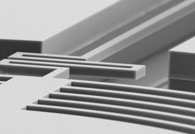
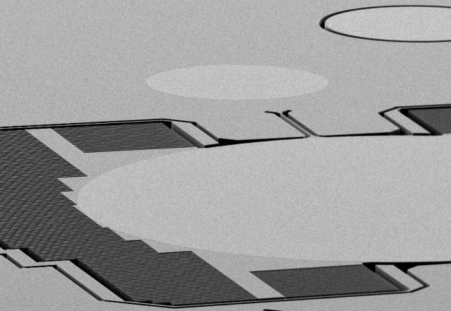
2 Introduction MicraGEM-Si is a process platform for MEMS prototyping and research offered by Micralyne Inc. This technology is a silicon-on-insulator (SOI) based MEMS process for academic and industrial users to develop devices such as micro mirrors, optical switches, resonators, inertial and bio sensors. The technology offers: Two thick SOI structure layers with up to three functional levels of silicon thickness on the Base device layer. The Top device layer has a silicon etch in the back side as well as a release etch from the top side. Deep etch features in the Base and the release etch in the Top device layer are aligned to better than 0.4 µm. This capability enables structures like vertical comb drive actuators. Base and Top device layers are electrically connected through the bond interface, allowing 3D routing of electrical signals. Patterned low-stress gold metallization on the top surface is suited for highly reflective mirrors and contact pads for gold wire bonding. Micralyne has partnered with CMC Microsystems to make this process available to companies and researchers as part of a Multi-Product Wafer program. This allows customers to purchase a portion of a MEMS fabrication run based on a 4 mm x 4 mm die size. Upon completion of the fabrication run, each client will receive a quantity of individual or packaged die. Larger die sizes are available by request (4 x 8 mm, 8 x 8 mm). CMC Microsystems provides the front end sales, delivery of the design kit, including a design rule checker, and the consolidation of designs for Micralyne to build. For design kit details and ordering visit: MicraGEM-Si Platform Description The process platform includes a powerful combination of established MEMS technologies. The Engineering team at Micralyne has leveraged its extensive experience in developing bulk machined MEMS devices to create a standard platform designed to enable a wide variety of MEMS structures. Key processes within the platform include high aspect ratio Deep Reactive Ion Etch (DRIE), aligned wafer to wafer bonding, non-contact stepper photolithography, and low stress mirror metallization. Stepper lithography provides non-contact exposures with excellent repeatability, consistency, alignment accuracy, throughput, and quality. Micralyne has demonstrated that silicon fingers in a precisely aligned staggered pattern can be maintained when using 3D wafer stacking. With thoughtful process design, out-of-plane features can be aligned to within 0.4 µm overlay tolerance. Figure 1: Vertical comb drive actuator


3 This process flow can used to create a vertical comb drive actuator, which is an important structure in the fabrication of advanced optical MEMS (Figure 1). The comb drive actuator provides nearly linear tilt response to the applied voltage at high angles. A well designed comb drive actuator can also significantly reduce the voltage requirement to achieve maximum tilt. MIcraGEM-Si Fabrication Flow Step 1: Define Trench 1, Trench 2 and Trench 3 on Base Wafer The device layer thickness of the Base wafer is 50 µm. The regions defined as Trench 1 are etched to a final depth of 50 µm (all the way through the device layer). Trench 2 regions are etched to a final depth of 35 µm, leaving a 15 µm high section of silicon sitting on the buried oxide of the Base SOI. Trench 3 regions are etched to a final depth of 10 µm, leaving a silicon region with a height of 40 µm sitting on the Base SOI. With these three regions, many complex 3D silicon structures can be created including cavities, electrodes and wires for electrical routing, as well as lower combs for vertical comb drive actuators. Step 2: Define and Etch Top SOI Wafer Backside The Top SOI wafer is patterned and etched to a depth of 20 µm. Once the Top SOI wafer is bonded and the handle wafer is removed, this will leave a suspended region of silicon with a 10 µm thickness. Step 3: Bond Base Wafer to Top Wafer Once the Base Wafer and Top wafer have completed the DRIE etch processes, the wafers are aligned and fusion bonded in a controlled environment. The accuracy of the wafer alignment after the completed fusion bond is +/-10 µm. Step 4: Remove Top SOI Handle and Buried Oxide After fusion bond, the handle of the Top wafer is removed with a grind and polish process. The buried oxide of the Top wafer is also removed leaving a pristine optically flat silicon surface.

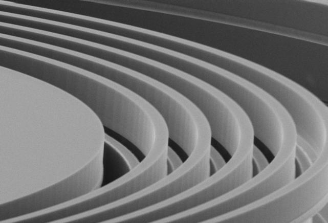
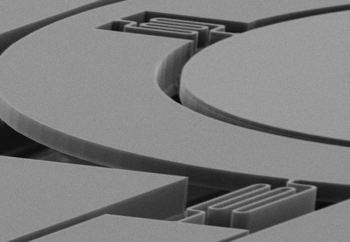
4 Step 5: Deposit and Define Metal The Top device layer is blanket coated with a low stress TiW/Au metallization. This is then patterned to form device elements such as electrodes, bond pads, and highly reflective surfaces. Step 6: Release Pattern and Etching The final DRIE process etches completely through the Top device layer and releases the MEMS structures. Step 7: Singulation The dicing process is done with a laser which enables singulation without Figure 2: damaging the released MEMS devices. MicraGEM-Si Process Example Variable Optical Attenuator (VOA) MEMS Chip The MicraGEM-Si platform is ideal for fabricating simple uni-directional (1D) tilting optical devices (Figure 3). These can be configured for use in variable optical attenuators (VOA) and low port count wavelength selective switch (WSS) modules. With the MicraGEM-Si platform you can create arrays of mirrors driven by vertical comb drives. The result is an array of mirrors requiring low actuation voltage and linear voltage-theta curve within its designed operating range (Figure 4). Figure 3: SEM Micrograph of the VOA Chip demo device
5 Mirror Tilt (Degrees) 0.7 Variable Optical Attenuator - Demo Design Circular mirror with one axis of tilt using vertical comb drive actuator Applied Voltage (Volts) Figure 4: MEMS for VOA - Mirror tilt response to an applied voltage The demonstration MEMS chip was designed to meet specific parameters for low voltage. Theoretically, a 1 mm diameter mirror can have a tilt of up to 4 degrees if voltage is not constrained. This platform is suitable for deflection of a mirror flat towards the Base wafer. Horizontal comb drives can also be created for use in inertial sensors. The creativity of the designers will also provide unlimited possibilities for structures, devices, and applications. Summary Micralyne has presented a process platform that provides the benefits of a vertical comb drive and other key MEMS structures, in an elegant and highly manufacturable format. Devices designed with MicraGEM-Si will be able to quickly ramp in to volume production.

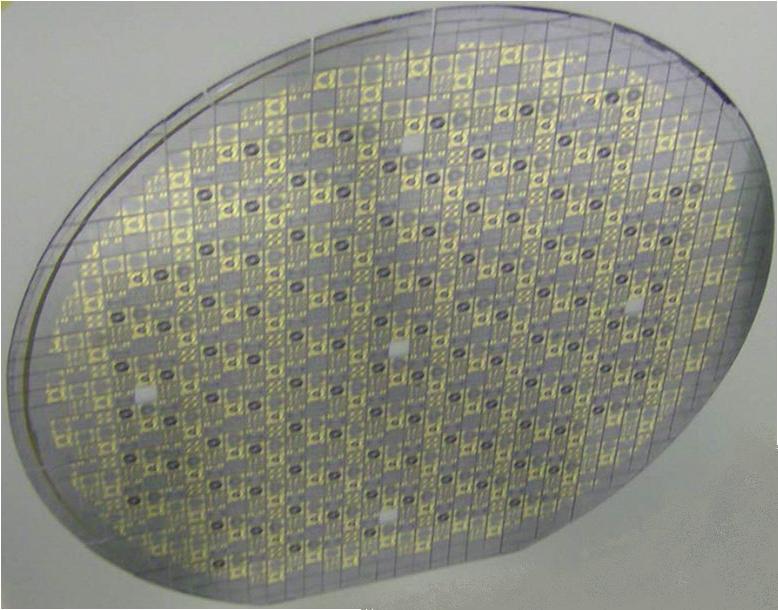
6 MicraGEM-Si TM Wafer
ksa MOS Ultra-Scan Performance Test Data
 ksa MOS Ultra-Scan Performance Test Data Introduction: ksa MOS Ultra Scan 200mm Patterned Silicon Wafers The ksa MOS Ultra Scan is a flexible, highresolution scanning curvature and tilt-measurement system.
9 rue Alfred Kastler - BP Nantes Cedex 3 - France Phone : +33 (0) website :
 website :") 9 rue Alfred Kastler - BP 10748-44307 Nantes Cedex 3 - France Phone : +33 (0) 240 180 916 - email : info@systemplus.fr - website : www.systemplus.fr August 2011 - Version 1 Written by: Sylvain HALLEREAU
9 rue Alfred Kastler - BP 10748-44307 Nantes Cedex 3 - France Phone : +33 (0) 240 180 916 - email : info@systemplus.fr - website : www.systemplus.fr August 2011 - Version 1 Written by: Sylvain HALLEREAU
LITHOGRAPHY CHALLENGES FOR LEADING EDGE 3D PACKAGING APPLICATIONS
 LITHOGRAPHY CHALLENGES FOR LEADING EDGE 3D PACKAGING APPLICATIONS Warren W. Flack, Manish Ranjan, Gareth Kenyon, Robert Hsieh Ultratech, Inc. 3050 Zanker Road, San Jose, CA 95134 USA mranjan@ultratech.com
Quilt Packaging Microchip Interconnect Technology
 Quilt Packaging Microchip Interconnect Technology 18 November 2012 Jason M. Kulick President, Co-Founder Indiana Integrated Circuits, LLC Overview Introduction to IIC Quilt Packaging (QP) Concept Electrical
SILICON-ON-INSULATOR (SOI) technology-based
 technology-based") 498 IEEE JOURNAL OF SELECTED TOPICS IN QUANTUM ELECTRONICS, VOL. 10, NO. 3, MAY/JUNE 2004 Vertical Combdrive Based 2-D Gimbaled Micromirrors With Large Static Rotation by Backside Island Isolation Sunghoon
498 IEEE JOURNAL OF SELECTED TOPICS IN QUANTUM ELECTRONICS, VOL. 10, NO. 3, MAY/JUNE 2004 Vertical Combdrive Based 2-D Gimbaled Micromirrors With Large Static Rotation by Backside Island Isolation Sunghoon
3D Process Modeling - A Novel and Efficient Tool for MEMS Foundry Design Support
 3D Process Modeling - A Novel and Efficient Tool for MEMS Foundry Design Support Gisbert Hölzer, Roy Knechtel X-FAB Semiconductor Foundries, AG Stephen Breit, Gerold Schropfer Coventor, Inc. Overview A
Applications, Processing and Integration Options for High Dielectric Constant Multi-Layer Thin-Film Barium Strontium Titanate (BST) Capacitors
 Capacitors") Applications, Processing and Integration Options for High Dielectric Constant Multi-Layer Thin-Film Barium Strontium Titanate (BST) Capacitors Agenda Introduction What is BST? Unique Characteristics of
Applications, Processing and Integration Options for High Dielectric Constant Multi-Layer Thin-Film Barium Strontium Titanate (BST) Capacitors Agenda Introduction What is BST? Unique Characteristics of
21 rue La Nouë Bras de Fer Nantes - France Phone : +33 (0) website :
 website :") 21 rue La Nouë Bras de Fer - 44200 Nantes - France Phone : +33 (0) 240 180 916 - email : info@systemplus.fr - website : www.systemplus.fr August 2012- Version 1 Written by: Maher SAHMIMI DISCLAIMER : System
21 rue La Nouë Bras de Fer - 44200 Nantes - France Phone : +33 (0) 240 180 916 - email : info@systemplus.fr - website : www.systemplus.fr August 2012- Version 1 Written by: Maher SAHMIMI DISCLAIMER : System
TES Detectors (and SQUID Muxes) at NIST
 at NIST") TES Detectors (and SQUID Muxes) at NIST Gene Hilton Kent Irwin William Duncan National Institute of Standards and Technology Boulder, Colorado December 13, 2006 Quantum Sensors Project Jim Beall Randy
TES Detectors (and SQUID Muxes) at NIST Gene Hilton Kent Irwin William Duncan National Institute of Standards and Technology Boulder, Colorado December 13, 2006 Quantum Sensors Project Jim Beall Randy
Case Studies of All-Surface Inspection in a 3DI-TSV R&D Environment. Rolf Shervey Sr. Applications Engineer Rudolph Technologies, Inc.
 Case Studies of All-Surface Inspection in a 3DI-TSV R&D Environment Rolf Shervey Sr. Applications Engineer Rudolph Technologies, Inc. Equipment in Albany Explorer Inspection Cluster AXi 935 for top surface
Comparison of Singulation Techniques
 Comparison of Singulation Techniques Electronic Packaging Society, Silicon Valley Chapter Sept. 28, 2017 ANNETTE TENG Sept 28, 2017 1 Definition of Singulation 9/28/2017 Annetteteng@promex-ind.com 2 www.cpmt.org/scv
AUTOFOCUS SENSORS & MICROSCOPY AUTOMATION IR LASER SCANNING CONFOCAL MICROSCOPE IRLC DEEP SEE. Now See Deeper than ever before
 AUTOFOCUS SENSORS & MICROSCOPY AUTOMATION IR LASER SCANNING CONFOCAL MICROSCOPE IRLC DEEP SEE Now See Deeper than ever before Review and inspection of non visible subsurface defects Non visible and subsurface
CLEAN ROOM TECHNOLOGY
 CLEAN ROOM TECHNOLOGY Justin Mathew Applied Electronics and Instrumentation College Of Engineering, Trivandrum April 28, 2015 Justin Mathew (CET) Clean Room Technology April 28, 2015 1 / 18 Overview 1
3D SYSTEM INTEGRATION TECHNOLOGY CHOICES AND CHALLENGE ERIC BEYNE, ANTONIO LA MANNA
 3D SYSTEM INTEGRATION TECHNOLOGY CHOICES AND CHALLENGE ERIC BEYNE, ANTONIO LA MANNA OUTLINE 3D Application Drivers and Roadmap 3D Stacked-IC Technology 3D System-on-Chip: Fine grain partitioning Conclusion
Bringing 3D Integration to Packaging Mainstream
 Bringing 3D Integration to Packaging Mainstream Enabling a Microelectronic World MEPTEC Nov 2012 Choon Lee Technology HQ, Amkor Highlighted TSV in Packaging TSMC reveals plan for 3DIC design based on silicon
TLS-Dicing for concentrator dies - a fast and clean technology. Hans-Ulrich Zühlke
 TLS-Dicing for concentrator dies - a fast and clean technology Hans-Ulrich Zühlke TLS-Dicing with JENOPTIK-VOTAN Semi Contents Overview Jenoptik Principle of TLS-Technology TLS-Dicing the benefits at a
MEMS PACKAGES AND MOUNTS GUIDE
 MEMS PACKAGES AND MOUNTS GUIDE Last Updated: 11/27/2017 Mirrorcle Technologies, Inc. Overview Mirrorcle Technologies Inc. ( MTI ) MEMS mirrors are available in the following standard ceramic packages:
9 rue Alfred Kastler - BP Nantes Cedex 3 - France Phone : +33 (0) website :
 website :") 9 rue Alfred Kastler - BP 10748-44307 Nantes Cedex 3 - France Phone : +33 (0) 240 180 916 - email : info@systemplus.fr - website : www.systemplus.fr May 2011 - Version 2 Written by: Sylvain HALLEREAU DISCLAIMER
9 rue Alfred Kastler - BP 10748-44307 Nantes Cedex 3 - France Phone : +33 (0) 240 180 916 - email : info@systemplus.fr - website : www.systemplus.fr May 2011 - Version 2 Written by: Sylvain HALLEREAU DISCLAIMER
Physical Design Implementation for 3D IC Methodology and Tools. Dave Noice Vassilios Gerousis
 I NVENTIVE Physical Design Implementation for 3D IC Methodology and Tools Dave Noice Vassilios Gerousis Outline 3D IC Physical components Modeling 3D IC Stack Configuration Physical Design With TSV Summary
Solidus Technologies, Inc. STI White Paper: AN092309R1
 STI White Paper: AN092309R1 Reduce your MEMS Package Level Final Test Times and Save MEMS Manufacturing Costs using STI3000 Wafer Level Test Technology Introduction A survey of MEMS manufacturing literature
OPTICAL TECHNOLOGIES FOR TSV INSPECTION Arun A. Aiyer, Frontier Semiconductor 2127 Ringwood Ave, San Jose, California 95131
 OPTICAL TECHNOLOGIES FOR TSV INSPECTION Arun A. Aiyer, Frontier Semiconductor 2127 Ringwood Ave, San Jose, California 95131 ABSTRACT: In this paper, Frontier Semiconductor will introduce a new technology
Quilt Packaging For Power Electronics
 Quilt Packaging For Power Electronics 21 March 2013 Jason M. Kulick President, Co-Founder Indiana Integrated Circuits, LLC Overview Introduction Quilt Packaging (QP) technology Concept Examples Advantages
SMAFTI Package Technology Features Wide-Band and Large-Capacity Memory
 SMAFTI Package Technology Features Wide-Band and Large-Capacity Memory KURITA Yoichiro, SOEJIMA Koji, KAWANO Masaya Abstract and NEC Corporation have jointly developed an ultra-compact system-in-package
Victory Process. Full Physical 3D Semiconductor Simulator Etching and Deposition Simulation
 Victory Process Full Physical 3D Semiconductor Simulator Etching and Deposition Simulation Victory Process 3D Process Simulator Victory Process provides the capability to simulate comprehensive full process
Micron Level Placement Accuracy for Wafer Scale Packaging of P-Side Down Lasers in Optoelectronic Products
 Micron Level Placement Accuracy for Wafer Scale Packaging of P-Side Down Lasers in Optoelectronic Products Daniel D. Evans, Jr. and Zeger Bok Palomar Technologies, Inc. 2728 Loker Avenue West Carlsbad,
EMPIR Grant Agreement 14IND07 3D Stack
 EMPIR Grant Agreement 14IND07 3D Stack Good Practice Guide: Recommendations on the strategy for measuring the dimensional properties of TSVs based on Confocal microscopy, IR interferometry and optical
SILICON PHOTONICS WAVEGUIDE AND ITS FIBER INTERCONNECT TECHNOLOGY. Jeong Hwan Song
 SILICON PHOTONICS WAVEGUIDE AND ITS FIBER INTERCONNECT TECHNOLOGY Jeong Hwan Song CONTENTS Introduction of light waveguides Principals Types / materials Si photonics Interface design between optical fiber
Speed, Accuracy and Automation in MEMS Simulation and Development C. J. Welham, Coventor, Paris
 Speed, Accuracy and Automation in MEMS Simulation and Development C. J. Welham, Coventor, Paris MEMS Design & Simulation Challenges Overview Simulation Challenges and Approaches Validation Case Studies
USABILITY OF CERAMIC STRUCTURES FOR POSITIONING OF OPTICAL MICRO ELEMENTS
 USABILITY OF CERAMIC STRUCTURES FOR POSITIONING OF OPTICAL MICRO ELEMENTS Holger Neubert, holger.neubert@ikts.fraunhofer.de, phone: +49 351 2553-7615 Fraunhofer Institute for Ceramic Technologies and Systems
3D systems-on-chip. A clever partitioning of circuits to improve area, cost, power and performance. The 3D technology landscape
 Edition April 2017 Semiconductor technology & processing 3D systems-on-chip A clever partitioning of circuits to improve area, cost, power and performance. In recent years, the technology of 3D integration
Discover 3D measurements for flexible electronics: a metrology masterclass
 Discover 3D measurements for flexible electronics: a metrology masterclass Samuel Lesko Bruker Nano Surfaces 21 November 2013 Smithers Pira the worldwide authority on the packaging, paper and print industry
Embedded UTCP interposers for miniature smart sensors
 Embedded UTCP interposers for miniature smart sensors T. Sterken 1,2, M. Op de Beeck 2, Tom Torfs 2, F. Vermeiren 1,2, C. Van Hoof 2, J. Vanfleteren 1,2 1 CMST (affiliated with Ugent and IMEC), Technologiepark
Polymer Micro-Optics for Today s Compact Photonic Devices
 Polymer Micro-Optics for Today s Compact Photonic Devices Lynn Dobosz - North America Sales & Business Development for the Opto-Electronic Systems business unit of the Optical Systems division of Jenoptik
MEMS SENSOR FOR MEMS METROLOGY
 MEMS SENSOR FOR MEMS METROLOGY IAB Presentation Byungki Kim, H Ali Razavi, F. Levent Degertekin, Thomas R. Kurfess 9/24/24 OUTLINE INTRODUCTION Motivation Contact/Noncontact measurement Optical interferometer
Magnetically actuated microshutter arrays
 Magnetically actuated microshutter arrays D. B. Mott *1, S.Aslam 1,2, K. A. Blumenstock 1, R. K. Fettig 1,2, D. Franz 1,2, A. S. Kutyrev 1,2, M. J. Li 1, C. J. Monroy 1,2, S. H. Moseley 1, D. S. Schwinger
반도체공정 - 김원정. Lattice constant (Å)
") 반도체물리 - 반도체공정 - 김원정 Semiconductors Lattice constant (Å) 1 PN junction Transistor 2 Integrated circuit Integrated circuit originally referred to a miniaturized electronic circuit consisting of semiconductor
반도체물리 - 반도체공정 - 김원정 Semiconductors Lattice constant (Å) 1 PN junction Transistor 2 Integrated circuit Integrated circuit originally referred to a miniaturized electronic circuit consisting of semiconductor
ULTRA-THIN DOUBLE LAYER METROLOGY WITH HIGH LATERAL RESOLUTION. Semicon West 2018, Bernd Srocka
 ULTRA-THIN DOUBLE LAYER METROLOGY WITH HIGH LATERAL RESOLUTION Semicon West 2018, Bernd Srocka Mission Unity-SC provides a wide range of Solutions in Metrology& inspection to the Semiconductor Industry,
AT&S Company. Presentation. 3D Component Packaging. in Organic Substrate. Embedded Component. Mark Beesley IPC Apex 2012, San Diego.
 3D Component Packaging AT&S Company in Organic Substrate Presentation Embedded Component Mark Beesley IPC Apex 2012, San Diego www.ats.net Austria Technologie & Systemtechnik Aktiengesellschaft Fabriksgasse13
Packaging and Integration Technologies for Silicon Photonics. Dr. Peter O Brien, Tyndall National Institute, Ireland.
 Packaging and Integration Technologies for Silicon Photonics Dr. Peter O Brien, Tyndall National Institute, Ireland. Opportunities for Silicon Photonics Stress Sensors Active Optical Cable 300 mm Silicon
2-DOF Actuated Micromirror Designed for Large DC Deflection
 2-DOF Actuated Micromirror Designed for Large DC Deflection Matthew Last, KSJ Pister Berkeley Sensor and Actuator Center 497 Cory Hall, UC Berkeley, Berkeley CA 94720-1770 ABSTRACT A 2 degree-of-freedom
Bulk MEMS Layout 2017 Dr. Lynn Fuller, Casey Gonta, Patsy Cadareanu Webpage:
 ROCHESTER INSTITUTE OF TECHNOLOGY MICROELECTRONIC ENGINEERING Bulk MEMS Layout 2017 Dr. Lynn Fuller, Casey Gonta, Patsy Cadareanu Webpage: http://people.rit.edu/lffeee 82 Lomb Memorial Drive Rochester,
Scanning Acoustic Microscopy For Metrology of 3D Interconnect Bonded Wafers
 Scanning Acoustic Microscopy For Metrology of 3D Interconnect Bonded Wafers Jim McKeon, Ph.D. - Sonix, Director of Technology Sriram Gopalan, Ph.D. - Sonix, Technology Engineer 8700 Morrissette Drive 8700
Electromagnetic Tip-tilt Mirror
 F L E X I B L E Flexible Optical B.V. Adaptive Optics Optical Microsystems Wavefront Sensors O P T I C A L Oleg Soloviev Chief Scientist Röntgenweg 1 2624 BD, Delft The Netherlands Tel: +31 15 285 15-47
37 (19) - channel micromachined deformable mirror system: typical technical passport
 - channel micromachined deformable mirror system: typical technical passport") F L E X I B L E Flexible Optical B.V. Adaptive Optics Optical Microsystems Wavefront Sensors O P T I C A L Oleg Soloviev Chief Scientist Röntgenweg 1 64 BD, Delft The Netherlands Tel: +31 1 1-4 Fax: +31
F L E X I B L E Flexible Optical B.V. Adaptive Optics Optical Microsystems Wavefront Sensors O P T I C A L Oleg Soloviev Chief Scientist Röntgenweg 1 64 BD, Delft The Netherlands Tel: +31 1 1-4 Fax: +31
Sony ICX098BL ¼ Inch Optical Format 5.6 µm Pixel Size CCD Image Sensor
 Sony ICX098BL ¼ Inch Optical Format 5.6 µm Pixel Size CCD Image Sensor Custom Imager Process Review For comments, questions, or more information about this report, or for any additional technical needs
Piezoelectric Tip-tilt Mirror
 F L E X I B L E Flexible Optical B.V. Adaptive Optics Optical Microsystems Wavefront Sensors O P T I C A L Oleg Soloviev Chief Scientist Röntgenweg 1 2624 BD, Delft The Netherlands Piezoelectric Tip-tilt
Metrology for Characterization of Wafer Thickness Uniformity During 3D-IC Processing. SEMATECH Workshop on 3D Interconnect Metrology
 Metrology for Characterization of Wafer Thickness Uniformity During 3D-IC Processing SEMATECH Workshop on 3D Interconnect Metrology Chris Lee July 11, 2012 Outline Introduction Motivation For New Metrology
Comparison & highlight on the last 3D TSV technologies trends Romain Fraux
 Comparison & highlight on the last 3D TSV technologies trends Romain Fraux Advanced Packaging & MEMS Project Manager European 3D Summit 18 20 January, 2016 Outline About System Plus Consulting 2015 3D
EECS 598: Integrating Emerging Technologies with Computer Architecture. Lecture 10: Three-Dimensional (3D) Integration
 Integration") 1 EECS 598: Integrating Emerging Technologies with Computer Architecture Lecture 10: Three-Dimensional (3D) Integration Instructor: Ron Dreslinski Winter 2016 University of Michigan 1 1 1 Announcements
1 EECS 598: Integrating Emerging Technologies with Computer Architecture Lecture 10: Three-Dimensional (3D) Integration Instructor: Ron Dreslinski Winter 2016 University of Michigan 1 1 1 Announcements
Assembly of thin gratings for soft x-ray telescopes
 Assembly of thin gratings for soft x-ray telescopes Mireille Akilian 1, Ralf K. Heilmann and Mark L. Schattenburg Space Nanotechnology Laboratory, MIT Kavli Institute for Astrophysics and Space Research,
Thin n-in-p planar pixel modules for the ATLAS upgrade at HL-LHC
 Thin n-in-p planar pixel modules for the ATLAS upgrade at HL-LHC A. Macchiolo, J. Beyer, A. La Rosa, R. Nisius, N. Savic Max-Planck-Institut für Physik, Munich 8 th International Workshop on Semiconductor
FABRICATION OF CMOS INTEGRATED CIRCUITS. Dr. Mohammed M. Farag
 FABRICATION OF CMOS INTEGRATED CIRCUITS Dr. Mohammed M. Farag Outline Overview of CMOS Fabrication Processes The CMOS Fabrication Process Flow Design Rules EE 432 VLSI Modeling and Design 2 CMOS Fabrication
Package (1C) Young Won Lim 3/20/13
 Young Won Lim 3/20/13") Copyright (c) 2011-2013 Young W. Lim. Permission is granted to copy, distribute and/or modify this document under the terms of the GNU Free Documentation License, Version 1.2 or any later version published
Copyright (c) 2011-2013 Young W. Lim. Permission is granted to copy, distribute and/or modify this document under the terms of the GNU Free Documentation License, Version 1.2 or any later version published
CHAPTER 4 DESIGN AND MODELING OF CANTILEVER BASED ELECTROSTATICALLY ACTUATED MICROGRIPPER WITH IMPROVED PERFORMANCE
 92 CHAPTER 4 DESIGN AND MODELING OF CANTILEVER BASED ELECTROSTATICALLY ACTUATED MICROGRIPPER WITH IMPROVED PERFORMANCE 4.1 INTRODUCTION Bio-manipulation techniques and tools including optical tweezers,
Defect Repair for EUVL Mask Blanks
 Defect Repair for EUVL Mask Blanks A.Barty, S.Hau-Riege, P.B.Mirkarimi, D.G.Stearns, H.Chapman, D.Sweeney Lawrence Livermore National Laboratory M.Clift Sandia National Laboratory E.Gullikson, M.Yi Lawrence
Influence of Geometrical Configuration of Cantilever Structure on Sensitivity of MEMS Resonant Sensors
 Influence of Geometrical Configuration of Cantilever Structure on Sensitivity of MEMS Resonant Sensors Georgeta Ionascu 1, Adriana Sandu 2, Elena Manea 3, Lucian Bogatu 4 1 Professor, Mechatronics & Precision
From 3D Toolbox to 3D Integration: Examples of Successful 3D Applicative Demonstrators N.Sillon. CEA. All rights reserved
 From 3D Toolbox to 3D Integration: Examples of Successful 3D Applicative Demonstrators N.Sillon Agenda Introduction 2,5D: Silicon Interposer 3DIC: Wide I/O Memory-On-Logic 3D Packaging: X-Ray sensor Conclusion
Optic fiber cores. mirror. fiber radius. centerline FMF. FMF distance. mirror tilt vs. necessary angular precision (fiber radius = 2 microns) 1.
 1.") Comparative Study of 2-DOF Micromirrors for Precision Light Manipulation Johanna I. Young and Andrei M. Shkel Microsystems Laboratory, Department of Mechanical and Aerospace Engineering, University of
Comparative Study of 2-DOF Micromirrors for Precision Light Manipulation Johanna I. Young and Andrei M. Shkel Microsystems Laboratory, Department of Mechanical and Aerospace Engineering, University of
Luxtera PN Silicon CMOS Photonic Chip Freescale 130 nm SOI CMOS Process
 Luxtera PN1000001 Silicon CMOS Photonic Chip Process Review 1891 Robertson Road, Suite 500, Ottawa, ON K2H 5B7 Canada Tel: 613-829-0414 www.chipworks.com Process Review Some of the information in this
edram to the Rescue Why edram 1/3 Area 1/5 Power SER 2-3 Fit/Mbit vs 2k-5k for SRAM Smaller is faster What s Next?
 edram to the Rescue Why edram 1/3 Area 1/5 Power SER 2-3 Fit/Mbit vs 2k-5k for SRAM Smaller is faster What s Next? 1 Integrating DRAM and Logic Integrate with Logic without impacting logic Performance,
2D nano PrintArray Product Data Sheet
 NSCRIPTOR Product Data Sheet Dip Pen Nanolithography (DPN ) is the process of writing nanoscale patterns of molecular "ink" onto a sample substrate via a coated SPM tip. NanoInk s NSCRIPTOR DPN System
Ultra-thin Capacitors for Enabling Miniaturized IoT Applications
 Ultra-thin Capacitors for Enabling Miniaturized IoT Applications Fraunhofer Demo Day, Oct 8 th, 2015 Konrad Seidel, Fraunhofer IPMS-CNT 10/15/2015 1 CONTENT Why we need thin passive devices? Integration
ION BEAM MILLING SYSTEM FOR TEM, SEM AND LM PREPARATION. Leica EM RES102
 ION BEAM MILLING SYSTEM FOR TEM, SEM AND LM PREPARATION Leica EM RES102 ION BEAM MILLING In recent years, ion milling has been developed into the most applicable method of sample preparation for the analysis
The Cornerstone Project:
 The Cornerstone Project: UK Silicon Photonics Fabrication Capability based on DUV Photolithography Dr Stevan Stanković University of Southampton Outline Introduction What is CORNERSTONE? What is offered?
Bringing Patterned Media to Production with Value Added Metrology
 Bringing Patterned Media to Production with Value Added Dean Dawson, Andrew S. Lopez Diskcon /IDEMA Conference, Session 6 September 24th, 2009 Overview Introduction AFM Scan Modes New Nanotrench Pattern
Hand book for use of library : Start_cmiV4
 Hand book for use of library : Start_cmiV4 The library of CMI for layout design has been up-dated, changes are : - V4.3 (27. Feb. 2008) o add cell ELECTRODEP_CIRCLE for electro-plating deposition o add
Package (1C) Young Won Lim 3/13/13
 Young Won Lim 3/13/13") Copyright (c) 2011-2013 Young W. Lim. Permission is granted to copy, distribute and/or modify this document under the terms of the GNU Free Documentation License, Version 1.2 or any later version published
Copyright (c) 2011-2013 Young W. Lim. Permission is granted to copy, distribute and/or modify this document under the terms of the GNU Free Documentation License, Version 1.2 or any later version published
Effective 3-D Process Modeling and Parameters Determination on Double Exposure in Deep X-ray Lithography
 Effective 3-D Process Modeling and Parameters Determination on Double Exposure in Deep X-ray Lithography Yoshikazu Hirai, Naoki Matsuzuka and Osamu Tabata Abstract This paper describes a new analytical
OPTIMIZATION OF THROUGH SI VIA LAST LITHOGRAPHY FOR 3D PACKAGING
 OPTIMIZATION OF THROUGH SI VIA LAST LITHOGRAPHY FOR 3D PACKAGING Warren W. Flack, Robert Hsieh, Gareth Kenyon Ultratech, Inc. 3050 Zanker Road, San Jose, CA 95134 USA wflack@ultratech.com John Slabbekoorn,
Advanced modelling of gratings in VirtualLab software. Site Zhang, development engineer Lignt Trans
 Advanced modelling of gratings in VirtualLab software Site Zhang, development engineer Lignt Trans 1 2 3 4 Content Grating Order Analyzer Rigorous Simulation of Holographic Generated Volume Grating Coupled
OPTI510R: Photonics. Khanh Kieu College of Optical Sciences, University of Arizona Meinel building R.626
 OPTI510R: Photonics Khanh Kieu College of Optical Sciences, University of Arizona kkieu@optics.arizona.edu Meinel building R.626 Important announcements Homework #2 is assigned, due Feb. 12 Travel to NSF
3D technology evolution to smart interposer and high density 3D ICs
 3D technology evolution to smart interposer and high density 3D ICs Patrick Leduc, Jean Charbonnier, Nicolas Sillon, Séverine Chéramy, Yann Lamy, Gilles Simon CEA-Leti, Minatec Campus Why 3D integration?
Beyond Chip Stacking---Quilt Packaging Enabled 3D Systems
 Beyond Chip Stacking---Quilt Packaging Enabled 3D Systems Jason Kulick, President & Co-Founder jason.kulick@indianaic.com 574-217-4612 (South Bend, IN) May 3, 2016 2016 New England IMAPS Symposium Presentation
UBCx Phot1x: Silicon Photonics Design, Fabrication and Data Analysis
 UBCx Phot1x: Silicon Photonics Design, Fabrication and Data Analysis Course Syllabus Table of Contents Course Syllabus 1 Course Overview 1 Course Learning Objective 1 Course Philosophy 1 Course Details
Laser Micro-Fabricator. Innovative Laser Technology KORTherm Science
 Laser Micro-Fabricator Innovative Laser Technology KORTherm Science Wavelength and material Interaction 10600n 1064nm 532nm 351nm 308nm 248nm 193nm 157nm N-H C-H O-H H-H O-O C-C N-O C-N N-N C-O THERMAL
ELASTOMERIC CONNECTORS. the smart solution for high-volume interconnections in compact design
 ELASTOMERIC CONNECTORS the smart solution for high-volume interconnections in compact design A NICE SIMPLE, RELIABLE CONNECTION How do elastomeric connectors work? STAX elastomers are zero insertion force
Development of innovative ALD materials for high density 3D integrated capacitors
 Development of innovative ALD materials for high density 3D integrated capacitors Malte Czernohorsky General Trend: System miniaturization Integration of passive components Capacitors Inductors Resistors
Non-destructive, High-resolution Fault Imaging for Package Failure Analysis. with 3D X-ray Microscopy. Application Note
 Non-destructive, High-resolution Fault Imaging for Package Failure Analysis with 3D X-ray Microscopy Application Note Non-destructive, High-resolution Fault Imaging for Package Failure Analysis with 3D
Epigap FAQs Part packges and form factors typical LED packages
 3. packges and form factors 3.1. typical LED packages Radiation from LEDs is generated by a semiconductor chip mounted in a package. LEDs are available in a variety of designs significantly influencing
Photoresist with Ultrasonic Atomization Allows for High-Aspect-Ratio Photolithography under Atmospheric Conditions
 Photoresist with Ultrasonic Atomization Allows for High-Aspect-Ratio Photolithography under Atmospheric Conditions 1 CONTRIBUTING AUTHORS Robb Engle, Vice President of Engineering, Sono-Tek Corporation
Advanced SAW Filter Technology
 Advanced SAW Filter Technology Advanced SAW Filter Technology Covering frequencies from MHz to 00 MHz API Technologies, a leading designer of precision RF and Microwave products, provides high performance
Maximum Clamping Voltage 8x20μs I/O to pin 2. Typical TLP Clamping Voltage (Note 1) I/O to GND I/O to I/O V RWM V I PP V I PP
 I/O to GND I/O to I/O V RWM V I PP V I PP") CPZ41X-CMKTVS5-4 4-Line Uni-Directional TVS/Diode Array Die 5.0 Volt The CPZ41X-CMKTVS5-4 is a silicon, low capacitance uni-directional transient voltage suppressor/diode array designed to protect four
CPZ41X-CMKTVS5-4 4-Line Uni-Directional TVS/Diode Array Die 5.0 Volt The CPZ41X-CMKTVS5-4 is a silicon, low capacitance uni-directional transient voltage suppressor/diode array designed to protect four
MEMS Deformable Mirror Actuators with Enhanced Reliability
 Invited Paper MEMS Deformable Mirror Actuators with Enhanced Reliability S.A. Cornelissen a, T.G. Bifano a,b, P.A. Bierden a a Boston Micromachines Corporation, 30 Spinelli Place, Cambridge, MA 02138,
CMOS compatible highly efficient grating couplers with a stair-step blaze profile
 CMOS compatible highly efficient grating couplers with a stair-step blaze profile Zhou Liang( ) a), Li Zhi-Yong( ) a), Hu Ying-Tao( ) a), Xiong Kang( ) a), Fan Zhong-Chao( ) b), Han Wei-Hua( ) b), Yu Yu-De
Increased Yield and Reliability of Packaged MEMS Resonator Devices. Carl Arft, Ph.D. Director of Test Dev. Engineering MEPTEC 2011
 Increased Yield and Reliability of Packaged MEMS Resonator Devices Carl Arft, Ph.D. Director of Test Dev. Engineering MEPTEC 2011 SiTime Summary $5B Timing Market 3 Segments Resonators, Oscillators, and
MEMS Pro v5.1 Layout Tutorial Physical Design Mask complexity
 MEMS Pro v5.1 Layout Tutorial 1 Physical Design Mask complexity MEMS masks are complex with curvilinear geometries Verification of manufacturing design rules is important Automatic generation of mask layout
March 15-18, 2015 Hilton Phoenix / Mesa Hotel Mesa, Arizona Archive Session 4
 Proceedings March 15-18, 2015 Hilton Phoenix / Mesa Hotel Mesa, Arizona Archive Session 4 2015 BiTS Workshop Image: BCFC/iStock Session 4 Rafiq Hussain Session Chair BiTS Workshop 2015 Schedule Performance
AIR FORCE INSTITUTE OF TECHNOLOGY
 Chip-to-Chip Optical Interconnection Using MEMS Mirrors THESIS Tod Laurvick, Captain, USAF AFIT/GE/ENG/09-27 DEPARTMENT OF THE AIR FORCE AIR UNIVERSITY AIR FORCE INSTITUTE OF TECHNOLOGY Wright-Patterson
Supplementary Materials for Superhydrophobic turbulent drag reduction as a function of surface grating parameters
 Supplementary Materials for Superhydrophobic turbulent drag reduction as a function of surface grating parameters Hyungmin Park, Guangyi Sun, and Chang-Jin CJ Kim Mechanical and Aerospace Engineering Department,
Sony ICX098BL ¼ Inch Optical Format 5.6 µm Pixel Size CCD Image Sensor
 Sony ICX098BL ¼ Inch Optical Format 5.6 µm Pixel Size CCD Image Sensor Substrate Dopant Analysis For comments, questions, or more information about this report, or for any additional technical needs concerning
OPTI510R: Photonics. Khanh Kieu College of Optical Sciences, University of Arizona Meinel building R.626
 OPTI510R: Photonics Khanh Kieu College of Optical Sciences, University of Arizona kkieu@optics.arizona.edu Meinel building R.626 Important announcements Homework #2 is assigned, due Feb. 11 Mid-term exam
Optimization of Photolithography Process Using Simulation
 Optimization of Photolithography Process Using Simulation Introduction The progress in semiconductor technology towards even smaller device geometries demands continuous refinements of photolithography
MPI TS2500-RF 200 mm Fully Automated Probe System For RF Production Test Measurements
 MPI TS2500-RF 200 mm Fully Automated Probe System For RF Production Test Measurements FEATURES / BENEFITS Designed for Wide Variety of RF On-Wafer Production Applications RF applications up to 67 GHz &
Doug Schramm a, Dale Bowles a, Martin Mastovich b, Paul C. Knutrud b, Anastasia Tyurina b ABSTRACT 1. INTRODUCTION
 Algorithm Implementation and Techniques for Providing More Reliable Overlay Measurements and Better Tracking of the Shallow Trench Isolation (STI) Process Doug Schramm a, Dale Bowles a, Martin Mastovich
Stress Reduction during Silicon Thinning Using Thermal Relaxation and 3D Curvature Correction Techniques
 Stress Reduction during Silicon Thinning Using Thermal Relaxation and 3D Curvature Correction Techniques Jim Colvin Consultant Heenal Patel, Timothy Hazeldine Ultra Tec Manufacturing, Santa Ana, USA Abstract
Schematic creation of MOS field effect transistor.
 Schematic creation of MOS field effect transistor. Gate electrode Drain electrode Source electrode Gate length Gate oxide A good reference is http://jas2.eng.buffalo.edu/applets/education/fab/nmos/nmos.html
A U T O C O L L I M A T O R S
 Printed in Germany 229 900 E 04/07 E l e c t r o n i c α A U T O C O L L I M A T O R S Measure With Precision MÖLLER-WEDEL OPTICAL GmbH Rosengarten 10 D-22880 Wedel Tel : +49-41 03-9 37 76 10 Fax: +49-41
Optical Topography Measurement of Patterned Wafers
 Optical Topography Measurement of Patterned Wafers Xavier Colonna de Lega and Peter de Groot Zygo Corporation, Laurel Brook Road, Middlefield CT 6455, USA xcolonna@zygo.com Abstract. We model the measurement
Mobility and Miniaturization 3D WLI Microscopes Address Key Metrology Needs
 Mobility and Miniaturization 3D WLI Microscopes Address Key Metrology Needs Outline Introductions Brief Overview of 3D Microscopes based on WLI General technology description Benefits and general applications
Ultrasonic Laserbonder M17
 PRODUCT-BROCHURE Ultrasonic Laserbonder M17 F & K DELVOTEC Partner for Tomorrow s Interconnection Technology. Developed in close co-operation with Fraunhofer Institute for Laser Technology in Aachen, the