Introduction to HW design flows
|
|
|
- Barnaby Greene
- 5 years ago
- Views:
Transcription

1 Graphics: Alexandra Nolte, Gesine Marwedel, 2003 Introduction to HW design flows
2 What you will get from this class This class will teach you how to use Hardware Description Languages (HDLs) to design, verify, and validate digital logic You will learn how to synthesize HDLs into hardware using the same tools used in industry (FPGA) You will participate in the always enlightening process of working to design a digital system in a team environment (optional) 2

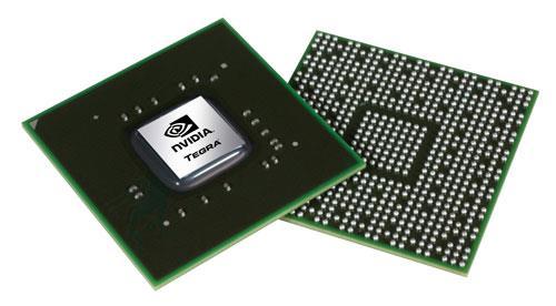


3 Mobile SoC

4 A SoC Example

5 System Design & Verification
6 Design Abstraction Levels Applications Generic Software Operating System Controlling Software Architecture HW/SW Interface System High-level organization Digital Logic Building-block Modules Logic Building-block Gates Circuit Transistors, Capacitors, etc. Devices & Interconnects Structures, interconnects Physics Electrons, Ions, etc. Software HW/SW Hardware
7 Moore s Law The velocity of IC complexity growth is proportional to IC complexity at the moment [Gordon Moore, 1964] Comparison coefficient: 0.2 for processors, 0.4 for memory Intel386 Processor Intel Itanium Processor Intel Pentium 4 Processor Intel Core i7 6x Intel Xeon 8x Sun SPARC T3 16-Core Intel Xeon 7500 Processor Dual Core Intel Itanium 2 Processor Intel Pentium Processor Intel486 Processor Intel Itanium 2 Processor Intel Pentium III Processor Intel Pentium II Processor Xilinx Virtex-7 6,800,000,000 transistors dn N dt N=digital estimation of complexity
8 Logic IC Gates (Chip) Universität Dortmund Evolution of Circuits Complexity 1M 100K Fujitsu Hitachi IBM NEC K 1K 100 Logic IC (gates/chip) 10times/5years M M-200H M-880 ACOS3800 M-1800 M-780 ES M M-680H 3090S ACOS2000 M-280H 64M M-380 ACOS M 4M DRAM (bits/chip) 4times/3years DRAM Bits/Chip H K 64K 1M Lithography (µm)


9 Complexity Evolution Intel Pentium IV Intel Core i7 stmere jpg microprocessor-set-to-produce.html
10 Application Specific Integrated Circuits (ASICs)
11 Hardware Implementations HDLs can be compiled to semi-custom and programmable hardware implementations Full Custom Semi- Custom Programmable Manual VLSI Standard Cell Gate Array FPGA less work, faster time to market implementation efficiency PLD 11
12 ASIC Application Specific Integrated Circuit A chip designed to perform a particular operation as opposed to General Purpose integrated circuits An ASIC is generally NOT software programmable to perform a wide variety of different tasks An ASIC will often have an embedded CPU to manage suitable tasks An ASIC may be implemented as an FPGA Sometimes considered a separate category
13 Examples of ASICs Video processor to decode or encode MPEG-2 digital TV signals Low power dedicated DSP/controller /convergence device for mobile phones Encryption processor for security Many examples of graphics chips Network processor for managing packets, traffic flow, etc.


14 ASIC Styles Full Custom ASICs Every transistor is designed and drawn by hand Typically only way to design analog portions of ASICs Gives the highest performance but the longest design time Full set of masks required for fabrication
 Standard-Cell-Based ASICs or Cell Based IC (CBIC) or semi-custom Standard Cells are custom designed and")

15 ASIC Styles (Contd.) Standard-Cell-Based ASICs or Cell Based IC (CBIC) or semi-custom Standard Cells are custom designed and then inserted into a library These cells are then used in the design by being placed in rows and wired together using place and route CAD tools Some standard cells, such as RAM and ROM cells, and some datapath cells (e.g. a multiplier) are tiled together to create macrocells D-flip-flop: NOR gate:
16 Standard Cell ASICs Sample ASIC floorplan: Standard Cell designs are usually synthesized from an RTL (Register Transfer Language) description of the design Intellectual Property Blocks (IPs) are often used to decrease Time to Market Hard IP (like SRAM): Technology Dependent, GDSII and libs Soft IP (DW library): Tech independent, delivered as RTL, with synthesis and verification scripts Standard-cell area (Soft Macro) Fixed blocks (Hard Macros) I/O cells
17 Standard Cell ASICs (cont d) Fabless semiconductor company model Company does design only. Fab performed by another company (e.g. TSMC, UMC, IBM, Philips, LSI). Back-end (place and route, etc.) might be performed at that company or with their assistance

18 FPGA Sample internal architecture: Store logic in look-up table (RAM) Programmable interconnect Programmable Interconnect Array: Configurable Logic Block (CLB):
19 FPGA (cont d)

20 Example Total cost calculation:
21 IC Cost The cost of non-recurrent engineering, NRE Design and mask preparation The cost factor of one time action The cost of recurrent engineering Semiconductor manufacturing, packaging, testing Proportional to size Proportional to IC area
22 NRE Value Increases Exploding NRE / Mask Costs Mask Costs (SM) ,05 0,1 0,15 0,2 Process Geometry (Micron) 70nm ASICs will have $4M NRE
 Source:")
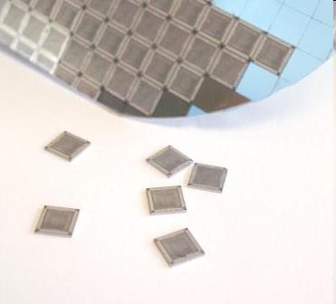
23 Die Value One die Wafer Up to 16 (40cm) Source: AMD
24 Yield Y N N g t 100% C D N C t W Y N t d A w d /2 2 d w 2 A d N t, N g total number and number of yield ICs on one wafer C W, C D - wafer and die cost D w wafer diameter, A d die area d
25 Defects Y 1 n d A d 4 D d ) C f(a n d number of defects on unit area, α-approximately 3
26 Comments Market currently dominated by standard cell ASICs and FPGAs Ideally standard cell designs would be used for higher volume applications that justify the Nonrecurring engineering (NRE) Many consider FPGAs separate from ASICs. Why? Different level of design skills required, especially in back end (place and route or physical design) Reduced level of verification required before sending to factory Again reduces sophistication required of team Low-cost (barrier) of entry Often different, lower cost Design Automation (CAD) tools Lower performance However, front-end design (RTL coding) is virtually identical for each implementation style Sometimes FPGA done first and standard cell ASIC done later
27 ASIC DESIGN FLOW
28 Electronics Design Spec System Design Hardware Design Software Design Integration Production Abstract Detailed Algorithm Design Architectural Design HW/SW Partitioning Analog/Digital Partitioning Specs Models Specs Models Analog Design Digital Design Mask Design Circuit Board Design Package Design Specs Models Hardware Hardware Host Coding Embedded Coding Software System Test Parts Lists Schematics Code Test Procedures Etc Manufacturin g Analysis and Verification Tasks Functional, Performance, Power, Cost, Reliability, Testability
29 ASIC Design Flow Major Steps: 1.High Level Design Specification Capture Design Capture in C, C++, SystemC or SystemVerilog (etc.) HW/SW partitioning IP selection (choose from pre-existing designs or Intellectual Property ) IP REUSE 2.RTL Design Register Transfer Level description 3.System, Timing and Logic Verification Is the logic working correctly?
30 ASIC Design Flow 4. Logic Synthesis 5. Physical Design Floorplanning, Place and Route, Clock insertion 6. Performance and Manufacturability Verification Extraction of Physical View (PEX) Design Rule Checking (DRC) Layout vs Schematic (LVS) Verification of timing and signal integrity
31 ASIC Design Flow Spec RTL Coding Synthesis Design For Test Floorplanning Place and Route Chip Finishing GDSII Digital Implementation HDL Coding (Verilog/VHDL ) RTL Synthesis Clock Gating Gate Optimization (DC, DCT) Scan Insertion Scan Compressio n JTAG Integration (DC,DCT) Virtual Flat Planning Power Mesh Creation Prototype Route and IPO Pin Assignment Macro Processing Budgeting (JXT) Placement Optimization HFNS, Clock Optimization Route Optimization Power Closure Timing Closure (PC,Astro) Design For Manufacturing (Astro, Hercules) Timing Closure (Astro) ECO (Astro) Iteration Analysis and Verification Design Rules, Functionality, Timing, Area, Power, Testability, Reliability, Manufacturability (Leda,VCS,Magellan,PrimeTime,Star-RCXT,Formality,PrimeTime-PX,Tetramax,PrimeRail,Hercules)
 between hardware registers, and the logical operations performed on those")
32 RTL Coding Register Transfer Level (RTL) is a way of describing the operation of a synchronous digital circuit Circuit's behavior is defined in terms of the flow of signals (or transfer of data) between hardware registers, and the logical operations performed on those signals.
 Simulations done to verify")
33 RTL Coding (Cntd) Most ASICs are designed using a RTL/Synthesis based methodology Design details captured in a simulatable description of the hardware Captured as Register Transfer Language (RTL) Simulations done to verify design
 2'b00: count <= count; 2'b01: // WRITE if (!")
 count <= count - 1; 2'b11: count <= count; endcase end end RTL Coding")
34 RTL Coding Spec clk) begin if (rstp == 1'b1) begin count <= 0; end else begin case ({readp, writep}) 2'b00: count <= count; 2'b01: // WRITE if (!fullp) count <= count + 1; 2'b10: // READ if (!emptyp) count <= count - 1; 2'b11: count <= count; endcase end end RTL Coding (Verilog/VHDL) VERIFICATION Meets Spec? No RTL Yes Synthesis
35 Verification Purpose of Verification: Discover as many potential bugs in the design as reasonable before sending chip out for fabrication Do this by simulating chip (and chip components) in Verilog Why is verification important? Chip fab might cost $4M and take 8 weeks Very expensive and time consuming to iterate chip fab! Want to get prototype correct in one to two fab cycles FPGAs can rely more on using the prototype for debug But, note, it is more difficult to debug hardware than a simulation
36 Verification (Cntd) Verification consumes more than 60% of design resources People, compute cycles Verification mainly done with pre-synthesis code Through some simulation, and other checks, are done to make sure the netlist is correct With increased reuse of existing Intellectual Property ( IP ), verification has become very challenging IP = Predesigned blocks, internally developed, purchased or obtained from open source Debugging is often harder than design! Focus of these Notes Primarily on verification tasks likely to be performed by module level designer, and code constructs commonly used
37 Verification Tools and Methods It is impossible to know that you have eliminated all the bugs in a design Thus it is important to use a variety of tools, techniques and methods that give you a high probability of discovering bugs And to have a plan to apply them! Get as many avenues of attack as possible Available tools and methods include: Simulation through test fixtures Including mixed level simulation Inserting and tracking assertions Formal verification Emulation
38 Simulations Through Test Fixtures Basic concept: Apply vectors to design as stimulus Observe outputs, and internal nodes, for correct functionality Key Questions: Where do you get the vectors? How do you observe the outputs? What are the available coding styles?

39 Functional Verification - RTL Behavioral simulation no delays for processing No performance parameters only functionality is verified Hardware description Not every construct in VHDL or Verilog can be implemented in hardware. This simulation will not show this.

40 Functional Verification Testbench

41 What is synthesis? The process of converting a hardware design described in a HDL into a structural netlist
42 In detail Design constraints Technology library (eg UMC 0.18) HDL Specification Module FSM(xx,xx) Begin xxx end HW inference Structural RTL (tech. Indep) Physical DA Logic Synthesis & Optimization Gate netlist

43 Logic Synthesis Automatic synthesis is used to turn the RTL into a gatelevel description ie. AND, OR gates, etc. Chip-test features are usually inserted at this point Gate level design verified for correctness Output of synthesis is a net-list i.e. List of logic gates and their implied connections NOR2 U36 (.Y(n107),.A0(n109),.A1(\value[2] ) ); NAND2 U37 (.Y(n109),.A0(n105),.A1(n103) ); NAND2 U38 (.Y(n114),.A0(\value[1] ),.A1(\value[0] ) ); NOR2 U39 (.Y(n115),.A0(\value[3] ),.A1(\value[2] ) );
44 Logic Synthesis Timing/Logic Library IP Library(DW) Physical Library RTL Timing Constraints Floorplan Synthesis (DC, DCT) residue = 16 h0000; if (high_bits == 2 b10) else residue = state_table[index]; state_table[index] = 16 h0000; Hardware Description Language (HDL) Synthesis HDL Translation Mapping Static Timing (DC/DCT/PC/PT) Formal Equivalence (FM) Power Analysis (DC/DCT/PC/PT-PX) Static Timing Placement Routing Estimation Meets Spec? No Optimization Design Rule Fixing Scan-Ready Netlist DFT Yes Target Technology (standard cells)
45 Floorplanning Corner cell I/O cell P/G buses Pad Die edge Bonding wire SOFT Macro Digital core Std Cell PLL RAM Leadframe Die Bonding Wire Core Area Resin mould Leadframe
 or a configuration")

46 Placement Physical Design tools used to turn the gate-level design into a set of chip masks (for photolithography) or a configuration file for downloading to an FPGA Floorplanning and Power Planning Positioning of major functions Placement of the Standard cells Gates arranged in rows

47 Clock Tree Synthesis (CTS) Clock and buffer Insertion Distribute clocks to cells and locate buffers for use as amplifiers in long wires


48 Routing Routing Logic Cells wired together Clock Routing Global Routing Detailed routing
49 Signoff & Chip Finishing Route Database Timing/Logic Library Hard Macro Library Physical Library Chip Finishing (Astro) Metal Fill Chip Finishing Double Via Insertion Filler Cell Insertion Critical Area Optimization Route Optimization STA with SI and SSTA for variations Antenna Fixing Route DRC Fixing IR drop and EM Analysis Design Rule Fixing Static Timing (PT/Star-RCXT) Formal Equiv (FM) Power Analysis (PTPX/PrimeRail) Route DRC (Hercules) LVS (Hercules) GDSII Meets Spec? Yes Mask Synthesis No GDSII

50 IC Fabrication General Technology Flow Diagram
.")
51 Lithography Lithography is a basic method of IC fabrication process. Process is used to transfer patterns from masks to each layer of the IC on the surface of a wafer by employing a photosensitive, chemically resistant layer (photoresist). Masks are created using the layout information provided by the designer. The lithographic process is repeated on each physical layer, but the process sequence is always the same:

52 Photolithography


53 Photolithography Equipment Resistors in photoresist pattern Resistors after etching Stepper (AMS Lithography) Wave length, nm NA Resolution, nm K ,60 0, ,58 0, ,57 0, ,57 0, ,75 0, ,39 0,35 The main characteristics of up to date steppers


54 PACKAGING Overview
Graphics: Alexandra Nolte, Gesine Marwedel, Universität Dortmund. RTL Synthesis
 Graphics: Alexandra Nolte, Gesine Marwedel, 2003 Universität Dortmund RTL Synthesis Purpose of HDLs Purpose of Hardware Description Languages: Capture design in Register Transfer Language form i.e. All
Design Methodologies and Tools. Full-Custom Design
 Design Methodologies and Tools Design styles Full-custom design Standard-cell design Programmable logic Gate arrays and field-programmable gate arrays (FPGAs) Sea of gates System-on-a-chip (embedded cores)
Chapter 5: ASICs Vs. PLDs
 Chapter 5: ASICs Vs. PLDs 5.1 Introduction A general definition of the term Application Specific Integrated Circuit (ASIC) is virtually every type of chip that is designed to perform a dedicated task.
Digital Design Methodology (Revisited) Design Methodology: Big Picture
 Design Methodology: Big Picture") Digital Design Methodology (Revisited) Design Methodology Design Specification Verification Synthesis Technology Options Full Custom VLSI Standard Cell ASIC FPGA CS 150 Fall 2005 - Lec #25 Design Methodology
Digital Design Methodology (Revisited) Design Methodology Design Specification Verification Synthesis Technology Options Full Custom VLSI Standard Cell ASIC FPGA CS 150 Fall 2005 - Lec #25 Design Methodology
Design Methodologies. Full-Custom Design
 Design Methodologies Design styles Full-custom design Standard-cell design Programmable logic Gate arrays and field-programmable gate arrays (FPGAs) Sea of gates System-on-a-chip (embedded cores) Design
Digital Design Methodology
 Digital Design Methodology Prof. Soo-Ik Chae Digital System Designs and Practices Using Verilog HDL and FPGAs @ 2008, John Wiley 1-1 Digital Design Methodology (Added) Design Methodology Design Specification
COE 561 Digital System Design & Synthesis Introduction
 1 COE 561 Digital System Design & Synthesis Introduction Dr. Aiman H. El-Maleh Computer Engineering Department King Fahd University of Petroleum & Minerals Outline Course Topics Microelectronics Design
FABRICATION TECHNOLOGIES
 FABRICATION TECHNOLOGIES DSP Processor Design Approaches Full custom Standard cell** higher performance lower energy (power) lower per-part cost Gate array* FPGA* Programmable DSP Programmable general
Hardware Design Environments. Dr. Mahdi Abbasi Computer Engineering Department Bu-Ali Sina University
 Hardware Design Environments Dr. Mahdi Abbasi Computer Engineering Department Bu-Ali Sina University Outline Welcome to COE 405 Digital System Design Design Domains and Levels of Abstractions Synthesis
DIGITAL DESIGN TECHNOLOGY & TECHNIQUES
 DIGITAL DESIGN TECHNOLOGY & TECHNIQUES CAD for ASIC Design 1 INTEGRATED CIRCUITS (IC) An integrated circuit (IC) consists complex electronic circuitries and their interconnections. William Shockley et
CS310 Embedded Computer Systems. Maeng
 1 INTRODUCTION (PART II) Maeng Three key embedded system technologies 2 Technology A manner of accomplishing a task, especially using technical processes, methods, or knowledge Three key technologies for
A VARIETY OF ICS ARE POSSIBLE DESIGNING FPGAS & ASICS. APPLICATIONS MAY USE STANDARD ICs or FPGAs/ASICs FAB FOUNDRIES COST BILLIONS
 architecture behavior of control is if left_paddle then n_state
EE 466/586 VLSI Design. Partha Pande School of EECS Washington State University
 EE 466/586 VLSI Design Partha Pande School of EECS Washington State University pande@eecs.wsu.edu Lecture 18 Implementation Methods The Design Productivity Challenge Logic Transistors per Chip (K) 10,000,000.10m
Spiral 2-8. Cell Layout
 2-8.1 Spiral 2-8 Cell Layout 2-8.2 Learning Outcomes I understand how a digital circuit is composed of layers of materials forming transistors and wires I understand how each layer is expressed as geometric
Overview. Design flow. Principles of logic synthesis. Logic Synthesis with the common tools. Conclusions
 Logic Synthesis Overview Design flow Principles of logic synthesis Logic Synthesis with the common tools Conclusions 2 System Design Flow Electronic System Level (ESL) flow System C TLM, Verification,
101-1 Under-Graduate Project Digital IC Design Flow
 101-1 Under-Graduate Project Digital IC Design Flow Speaker: Ming-Chun Hsiao Adviser: Prof. An-Yeu Wu Date: 2012/9/25 ACCESS IC LAB Outline Introduction to Integrated Circuit IC Design Flow Verilog HDL
Overview of Digital Design Methodologies
 Overview of Digital Design Methodologies ELEC 5402 Pavan Gunupudi Dept. of Electronics, Carleton University January 5, 2012 1 / 13 Introduction 2 / 13 Introduction Driving Areas: Smart phones, mobile devices,
VLSI Design Automation
 VLSI Design Automation IC Products Processors CPU, DSP, Controllers Memory chips RAM, ROM, EEPROM Analog Mobile communication, audio/video processing Programmable PLA, FPGA Embedded systems Used in cars,
EITF35: Introduction to Structured VLSI Design
 EITF35: Introduction to Structured VLSI Design Part 1.1.2: Introduction (Digital VLSI Systems) Liang Liu liang.liu@eit.lth.se 1 Outline Why Digital? History & Roadmap Device Technology & Platforms System
VLSI Design Automation
 VLSI Design Automation IC Products Processors CPU, DSP, Controllers Memory chips RAM, ROM, EEPROM Analog Mobile communication, audio/video processing Programmable PLA, FPGA Embedded systems Used in cars,
Lab. Course Goals. Topics. What is VLSI design? What is an integrated circuit? VLSI Design Cycle. VLSI Design Automation
 Course Goals Lab Understand key components in VLSI designs Become familiar with design tools (Cadence) Understand design flows Understand behavioral, structural, and physical specifications Be able to
CAD for VLSI. Debdeep Mukhopadhyay IIT Madras
 CAD for VLSI Debdeep Mukhopadhyay IIT Madras Tentative Syllabus Overall perspective of VLSI Design MOS switch and CMOS, MOS based logic design, the CMOS logic styles, Pass Transistors Introduction to Verilog
FPGA: What? Why? Marco D. Santambrogio
 FPGA: What? Why? Marco D. Santambrogio marco.santambrogio@polimi.it 2 Reconfigurable Hardware Reconfigurable computing is intended to fill the gap between hardware and software, achieving potentially much
VLSI Design Automation. Maurizio Palesi
 VLSI Design Automation 1 Outline Technology trends VLSI Design flow (an overview) 2 Outline Technology trends VLSI Design flow (an overview) 3 IC Products Processors CPU, DSP, Controllers Memory chips
Design Methodologies
 Design Methodologies 1981 1983 1985 1987 1989 1991 1993 1995 1997 1999 2001 2003 2005 2007 2009 Complexity Productivity (K) Trans./Staff - Mo. Productivity Trends Logic Transistor per Chip (M) 10,000 0.1
Workspace for '4-FPGA' Page 1 (row 1, column 1)
") Workspace for '4-FPGA' Page 1 (row 1, column 1) Workspace for '4-FPGA' Page 2 (row 2, column 1) Workspace for '4-FPGA' Page 3 (row 3, column 1) ECEN 449 Microprocessor System Design FPGAs and Reconfigurable
Workspace for '4-FPGA' Page 1 (row 1, column 1) Workspace for '4-FPGA' Page 2 (row 2, column 1) Workspace for '4-FPGA' Page 3 (row 3, column 1) ECEN 449 Microprocessor System Design FPGAs and Reconfigurable
FPGA for Complex System Implementation. National Chiao Tung University Chun-Jen Tsai 04/14/2011
 FPGA for Complex System Implementation National Chiao Tung University Chun-Jen Tsai 04/14/2011 About FPGA FPGA was invented by Ross Freeman in 1989 SRAM-based FPGA properties Standard parts Allowing multi-level
Bibliography. Measuring Software Reuse, Jeffrey S. Poulin, Addison-Wesley, Practical Software Reuse, Donald J. Reifer, Wiley, 1997.
 Bibliography Books on software reuse: 1. 2. Measuring Software Reuse, Jeffrey S. Poulin, Addison-Wesley, 1997. Practical Software Reuse, Donald J. Reifer, Wiley, 1997. Formal specification and verification:
E 4.20 Introduction to Digital Integrated Circuit Design
 E 4.20 Introduction to Digital Integrated Circuit Design Peter Cheung Department of Electrical & Electronic Engineering Imperial College London URL: www.ee.ic.ac.uk/pcheung/ E-mail: p.cheung@imperial.ac.uk
Introduction to ASICs. ni logic Pvt. Ltd., Pune
 Introduction to ASICs ni logic Pvt. Ltd., Pune The Wonderful World of Silicon About every two years, the number of transistors on a CMOS silicon chip doubles and the clock speed doubles..this rate of improvement
ECEN 449 Microprocessor System Design. FPGAs and Reconfigurable Computing
 ECEN 449 Microprocessor System Design FPGAs and Reconfigurable Computing Some of the notes for this course were developed using the course notes for ECE 412 from the University of Illinois, Urbana-Champaign
VLSI Design Automation. Calcolatori Elettronici Ing. Informatica
 VLSI Design Automation 1 Outline Technology trends VLSI Design flow (an overview) 2 IC Products Processors CPU, DSP, Controllers Memory chips RAM, ROM, EEPROM Analog Mobile communication, audio/video processing
Outline. EECS150 - Digital Design Lecture 6 - Field Programmable Gate Arrays (FPGAs) FPGA Overview. Why FPGAs?
 FPGA Overview. Why FPGAs?") EECS150 - Digital Design Lecture 6 - Field Programmable Gate Arrays (FPGAs) September 12, 2002 John Wawrzynek Outline What are FPGAs? Why use FPGAs (a short history lesson). FPGA variations Internal logic
EECS150 - Digital Design Lecture 6 - Field Programmable Gate Arrays (FPGAs) September 12, 2002 John Wawrzynek Outline What are FPGAs? Why use FPGAs (a short history lesson). FPGA variations Internal logic
PrimeTime: Introduction to Static Timing Analysis Workshop
 i-1 PrimeTime: Introduction to Static Timing Analysis Workshop Synopsys Customer Education Services 2002 Synopsys, Inc. All Rights Reserved PrimeTime: Introduction to Static 34000-000-S16 Timing Analysis
An Introduction to Programmable Logic
 Outline An Introduction to Programmable Logic 3 November 24 Transistors Logic Gates CPLD Architectures FPGA Architectures Device Considerations Soft Core Processors Design Example Quiz Semiconductors Semiconductor
EE 434 ASIC & Digital Systems
 EE 434 ASIC & Digital Systems Dae Hyun Kim EECS Washington State University Spring 2018 Course Website http://eecs.wsu.edu/~ee434 Themes Study how to design, analyze, and test a complex applicationspecific
An Overview of Standard Cell Based Digital VLSI Design
 An Overview of Standard Cell Based Digital VLSI Design With examples taken from the implementation of the 36-core AsAP1 chip and the 1000-core KiloCore chip Zhiyi Yu, Tinoosh Mohsenin, Aaron Stillmaker,
FPGA Based Digital Design Using Verilog HDL
 FPGA Based Digital Design Using Course Designed by: IRFAN FAISAL MIR ( Verilog / FPGA Designer ) irfanfaisalmir@yahoo.com * Organized by Electronics Division Integrated Circuits Uses for digital IC technology
ECE U530 Digital Hardware Synthesis. What is the course about?
 ECE U530 Digital Hardware Synthesis Prof. Miriam Leeser mel@coe.neu.edu Sept 6, 2006 Lecture 1: Overview Organization What is an ASIC? Why FPGAs? Hardware Description Languages and VHDL ECE U530 F06 What
AMS DESIGN METHODOLOGY
 OVER VIEW CADENCE ANALOG/ MIXED-SIGNAL DESIGN METHODOLOGY The Cadence Analog/Mixed-Signal (AMS) Design Methodology employs advanced Cadence Virtuoso custom design technologies and leverages silicon-accurate
An overview of standard cell based digital VLSI design
 An overview of standard cell based digital VLSI design Implementation of the first generation AsAP processor Zhiyi Yu and Tinoosh Mohsenin VCL Laboratory UC Davis Outline Overview of standard cellbased
Overview. CSE372 Digital Systems Organization and Design Lab. Hardware CAD. Two Types of Chips
 Overview CSE372 Digital Systems Organization and Design Lab Prof. Milo Martin Unit 5: Hardware Synthesis CAD (Computer Aided Design) Use computers to design computers Virtuous cycle Architectural-level,
Evolution of CAD Tools & Verilog HDL Definition
 Evolution of CAD Tools & Verilog HDL Definition K.Sivasankaran Assistant Professor (Senior) VLSI Division School of Electronics Engineering VIT University Outline Evolution of CAD Different CAD Tools for
EECS150 - Digital Design Lecture 6 - Field Programmable Gate Arrays (FPGAs)
") EECS150 - Digital Design Lecture 6 - Field Programmable Gate Arrays (FPGAs) September 12, 2002 John Wawrzynek Fall 2002 EECS150 - Lec06-FPGA Page 1 Outline What are FPGAs? Why use FPGAs (a short history
EECS150 - Digital Design Lecture 6 - Field Programmable Gate Arrays (FPGAs) September 12, 2002 John Wawrzynek Fall 2002 EECS150 - Lec06-FPGA Page 1 Outline What are FPGAs? Why use FPGAs (a short history
Implementing Tile-based Chip Multiprocessors with GALS Clocking Styles
 Implementing Tile-based Chip Multiprocessors with GALS Clocking Styles Zhiyi Yu, Bevan Baas VLSI Computation Lab, ECE Department University of California, Davis, USA Outline Introduction Timing issues
RTL Coding General Concepts
 RTL Coding General Concepts Typical Digital System 2 Components of a Digital System Printed circuit board (PCB) Embedded d software microprocessor microcontroller digital signal processor (DSP) ASIC Programmable
Design Methodologies. Digital Integrated Circuits A Design Perspective. Jan M. Rabaey Anantha Chandrakasan Borivoje Nikolic.
 Digital Integrated Circuits A Design Perspective Jan M. Rabaey Anantha Chandrakasan Borivoje Nikolic Design Methodologies December 10, 2002 L o g i c T r a n s i s t o r s p e r C h i p ( K ) 1 9 8 1 1
UNIT 4 INTEGRATED CIRCUIT DESIGN METHODOLOGY E5163
 UNIT 4 INTEGRATED CIRCUIT DESIGN METHODOLOGY E5163 LEARNING OUTCOMES 4.1 DESIGN METHODOLOGY By the end of this unit, student should be able to: 1. Explain the design methodology for integrated circuit.
Evolution of Implementation Technologies. ECE 4211/5211 Rapid Prototyping with FPGAs. Gate Array Technology (IBM s) Programmable Logic
 Programmable Logic") ECE 42/52 Rapid Prototyping with FPGAs Dr. Charlie Wang Department of Electrical and Computer Engineering University of Colorado at Colorado Springs Evolution of Implementation Technologies Discrete devices:
ECE 42/52 Rapid Prototyping with FPGAs Dr. Charlie Wang Department of Electrical and Computer Engineering University of Colorado at Colorado Springs Evolution of Implementation Technologies Discrete devices:
Hardware Synthesis. References
 Hardware Synthesis MidiaReshadi CE Department Science and research branch of Islamic Azad University Email: ce.srbiau@gmail.com 1 References 2 1 Chapter 1 Digital Design Using VHDL and PLDs 3 Some Definitions
Cell-Based Design Flow. TA : 吳廸優
 Cell-Based Design Flow TA : 吳廸優 dywu@viplab.cs.nctu.edu.tw 1 Outline Overview Design Flow Stage 1 RTL Development Synthesis Gate Level Simulation Design Flow Stage 2 Placement and Routing Post Layout Simulation
System on Chip (SoC) Design
 Design") System on Chip (SoC) Design Moore s Law and Technology Scaling the performance of an IC, including the number components on it, doubles every 18-24 months with the same chip price... - Gordon Moore - 1960
System on Chip (SoC) Design Moore s Law and Technology Scaling the performance of an IC, including the number components on it, doubles every 18-24 months with the same chip price... - Gordon Moore - 1960
TOPIC : Verilog Synthesis examples. Module 4.3 : Verilog synthesis
 TOPIC : Verilog Synthesis examples Module 4.3 : Verilog synthesis Example : 4-bit magnitude comptarator Discuss synthesis of a 4-bit magnitude comparator to understand each step in the synthesis flow.
ECE 459/559 Secure & Trustworthy Computer Hardware Design
 ECE 459/559 Secure & Trustworthy Computer Hardware Design VLSI Design Basics Garrett S. Rose Spring 2016 Recap Brief overview of VHDL Behavioral VHDL Structural VHDL Simple examples with VHDL Some VHDL
Xilinx SSI Technology Concept to Silicon Development Overview
 Xilinx SSI Technology Concept to Silicon Development Overview Shankar Lakka Aug 27 th, 2012 Agenda Economic Drivers and Technical Challenges Xilinx SSI Technology, Power, Performance SSI Development Overview
More Course Information
 More Course Information Labs and lectures are both important Labs: cover more on hands-on design/tool/flow issues Lectures: important in terms of basic concepts and fundamentals Do well in labs Do well
EE-382M VLSI II. Early Design Planning: Front End
 EE-382M VLSI II Early Design Planning: Front End Mark McDermott EE 382M-8 VLSI-2 Page Foil # 1 1 EDP Objectives Get designers thinking about physical implementation while doing the architecture design.
Chapter 1 Overview of Digital Systems Design
 Chapter 1 Overview of Digital Systems Design SKEE2263 Digital Systems Mun im/ismahani/izam {munim@utm.my,e-izam@utm.my,ismahani@fke.utm.my} February 8, 2017 Why Digital Design? Many times, microcontrollers
COEN-4730 Computer Architecture Lecture 12. Testing and Design for Testability (focus: processors)
") 1 COEN-4730 Computer Architecture Lecture 12 Testing and Design for Testability (focus: processors) Cristinel Ababei Dept. of Electrical and Computer Engineering Marquette University 1 Outline Testing
1 COEN-4730 Computer Architecture Lecture 12 Testing and Design for Testability (focus: processors) Cristinel Ababei Dept. of Electrical and Computer Engineering Marquette University 1 Outline Testing
Digital System Design Lecture 2: Design. Amir Masoud Gharehbaghi
 Digital System Design Lecture 2: Design Amir Masoud Gharehbaghi amgh@mehr.sharif.edu Table of Contents Design Methodologies Overview of IC Design Flow Hardware Description Languages Brief History of HDLs
Hardware Modeling using Verilog Prof. Indranil Sengupta Department of Computer Science and Engineering Indian Institute of Technology, Kharagpur
 Hardware Modeling using Verilog Prof. Indranil Sengupta Department of Computer Science and Engineering Indian Institute of Technology, Kharagpur Lecture 01 Introduction Welcome to the course on Hardware
ASIC Physical Design Top-Level Chip Layout
 ASIC Physical Design Top-Level Chip Layout References: M. Smith, Application Specific Integrated Circuits, Chap. 16 Cadence Virtuoso User Manual Top-level IC design process Typically done before individual
IP CORE Design 矽智產設計. C. W. Jen 任建葳.
 IP CORE Design 矽智產設計 C. W. Jen 任建葳 cwjen@twins.ee.nctu.edu.tw Course Contents Introduction to SoC and IP ARM processor core and instruction sets VCI interface, on-chip bus, and platform-based design IP
ASIC, Customer-Owned Tooling, and Processor Design
 ASIC, Customer-Owned Tooling, and Processor Design Design Style Myths That Lead EDA Astray Nancy Nettleton Manager, VLSI ASIC Device Engineering April 2000 Design Style Myths COT is a design style that
Overview of Digital Design with Verilog HDL 1
 Overview of Digital Design with Verilog HDL 1 1.1 Evolution of Computer-Aided Digital Design Digital circuit design has evolved rapidly over the last 25 years. The earliest digital circuits were designed
Design of DMA Controller Using VHDL
 Design of DMA Controller Using VHDL Rashmi mishra 1, Rupal chauhan 2, Garima arora 3 1, 2 Department of Electronics & Communication BE (VII SEM) Takshshila Institute of Engineering & Technology, Jabalpur,
Intro to High Level Design with SystemC
 Intro to High Level Design with SystemC Aim To introduce SystemC, and its associated Design Methodology Date 26th March 2001 Presented By Alan Fitch Designer Challenges Design complexity System on Chip
CHAPTER 1 INTRODUCTION
 CHAPTER 1 INTRODUCTION Rapid advances in integrated circuit technology have made it possible to fabricate digital circuits with large number of devices on a single chip. The advantages of integrated circuits
Introduction. Sungho Kang. Yonsei University
 Introduction Sungho Kang Yonsei University Outline VLSI Design Styles Overview of Optimal Logic Synthesis Model Graph Algorithm and Complexity Asymptotic Complexity Brief Summary of MOS Device Behavior
Silicon Virtual Prototyping: The New Cockpit for Nanometer Chip Design
 Silicon Virtual Prototyping: The New Cockpit for Nanometer Chip Design Wei-Jin Dai, Dennis Huang, Chin-Chih Chang, Michel Courtoy Cadence Design Systems, Inc. Abstract A design methodology for the implementation
INTRODUCTION TO FPGA ARCHITECTURE
 3/3/25 INTRODUCTION TO FPGA ARCHITECTURE DIGITAL LOGIC DESIGN (BASIC TECHNIQUES) a b a y 2input Black Box y b Functional Schematic a b y a b y a b y 2 Truth Table (AND) Truth Table (OR) Truth Table (XOR)
Outline. SoC Encounter Flow. Typical Backend Design Flow. Digital IC-Project and Verification. Place and Route. Backend ASIC Design flow
 Outline Digital IC-Project and Verification Deepak Dasalukunte Backend ASIC Design flow General steps Input files Floorplanning Placement Clock-synthesis Routing Typical Backend Design Flow SoC Encounter
ECE 111 ECE 111. Advanced Digital Design. Advanced Digital Design Winter, Sujit Dey. Sujit Dey. ECE Department UC San Diego
 Advanced Digital Winter, 2009 ECE Department UC San Diego dey@ece.ucsd.edu http://esdat.ucsd.edu Winter 2009 Advanced Digital Objective: of a hardware-software embedded system using advanced design methodologies
Trend in microelectronics The design process and tasks Different design paradigms Basic terminology The test problems
 Electronics Systems Trend in microelectronics The design process and tasks Different design paradigms Basic terminology The test problems The Technological Trend # of trans. 100M 75M 50M Moore s Law (#
Case study of Mixed Signal Design Flow
 IOSR Journal of VLSI and Signal Processing (IOSR-JVSP) Volume 6, Issue 3, Ver. II (May. -Jun. 2016), PP 49-53 e-issn: 2319 4200, p-issn No. : 2319 4197 www.iosrjournals.org Case study of Mixed Signal Design
Introduction Lecturer: Gil Rahav Semester B, EE Dept. BGU. Freescale Semiconductors Israel
 Design מבוא לתכנון VLSI ספרתי Introduction Lecturer: Semester B, EE Dept. BGU. Freescale Semiconductors Israel 1 IC Products Processors CPU, DSP, Controllers Memory chips RAM, ROM, EEPROM Analog Mobile
PLAs & PALs. Programmable Logic Devices (PLDs) PLAs and PALs
 PLAs and PALs") PLAs & PALs Programmable Logic Devices (PLDs) PLAs and PALs PLAs&PALs By the late 1970s, standard logic devices were all the rage, and printed circuit boards were loaded with them. To offer the ultimate
PLAs & PALs Programmable Logic Devices (PLDs) PLAs and PALs PLAs&PALs By the late 1970s, standard logic devices were all the rage, and printed circuit boards were loaded with them. To offer the ultimate
Design Solutions in Foundry Environment. by Michael Rubin Agilent Technologies
 Design Solutions in Foundry Environment by Michael Rubin Agilent Technologies Presenter: Michael Rubin RFIC Engineer, R&D, Agilent Technologies former EDA Engineering Manager Agilent assignee at Chartered
SoC Verification Methodology. Prof. Chien-Nan Liu TEL: ext:
 SoC Verification Methodology Prof. Chien-Nan Liu TEL: 03-4227151 ext:4534 Email: jimmy@ee.ncu.edu.tw 1 Outline l Verification Overview l Verification Strategies l Tools for Verification l SoC Verification
Park Sung Chul. AE MentorGraphics Korea
 PGA Design rom Concept to Silicon Park Sung Chul AE MentorGraphics Korea The Challenge of Complex Chip Design ASIC Complex Chip Design ASIC or FPGA? N FPGA Design FPGA Embedded Core? Y FPSoC Design Considerations
Verilog. What is Verilog? VHDL vs. Verilog. Hardware description language: Two major languages. Many EDA tools support HDL-based design
 Verilog What is Verilog? Hardware description language: Are used to describe digital system in text form Used for modeling, simulation, design Two major languages Verilog (IEEE 1364), latest version is
Hardware Modelling. Design Flow Overview. ECS Group, TU Wien
 Hardware Modelling Design Flow Overview ECS Group, TU Wien 1 Outline Difference: Hardware vs. Software Design Flow Steps Specification Realisation Verification FPGA Design Flow 2 Hardware vs. Software:
INTRODUCTION TO FIELD PROGRAMMABLE GATE ARRAYS (FPGAS)
") INTRODUCTION TO FIELD PROGRAMMABLE GATE ARRAYS (FPGAS) Bill Jason P. Tomas Dept. of Electrical and Computer Engineering University of Nevada Las Vegas FIELD PROGRAMMABLE ARRAYS Dominant digital design
INTRODUCTION TO FIELD PROGRAMMABLE GATE ARRAYS (FPGAS) Bill Jason P. Tomas Dept. of Electrical and Computer Engineering University of Nevada Las Vegas FIELD PROGRAMMABLE ARRAYS Dominant digital design
Lecture Content. 1 Adam Teman, 2018
 Lecture Content 1 Adam Teman, 2018 Digital VLSI Design Lecture 6: Moving to the Physical Domain Semester A, 2018-19 Lecturer: Dr. Adam Teman December 24, 2018 Disclaimer: This course was prepared, in its
Philip Andrew Simpson. FPGA Design. Best Practices for Team-based Reuse. Second Edition
 FPGA Design Philip Andrew Simpson FPGA Design Best Practices for Team-based Reuse Second Edition Philip Andrew Simpson San Jose, CA, USA ISBN 978-3-319-17923-0 DOI 10.1007/978-3-319-17924-7 ISBN 978-3-319-17924-7
Lecture #1: Introduction
 Lecture #1: Introduction Kunle Olukotun Stanford EE183 January 8, 20023 What is EE183? EE183 is continuation of EE121 Digital Logic Design is a a minute to learn, a lifetime to master Programmable logic
PINE TRAINING ACADEMY
 PINE TRAINING ACADEMY Course Module A d d r e s s D - 5 5 7, G o v i n d p u r a m, G h a z i a b a d, U. P., 2 0 1 0 1 3, I n d i a Digital Logic System Design using Gates/Verilog or VHDL and Implementation
Organization. 5.1 Semiconductor Main Memory. William Stallings Computer Organization and Architecture 6th Edition
 William Stallings Computer Organization and Architecture 6th Edition Chapter 5 Internal Memory 5.1 Semiconductor Main Memory 5.2 Error Correction 5.3 Advanced DRAM Organization 5.1 Semiconductor Main Memory
System-on-Chip Design for Wireless Communications
 System-on-Chip Design for Wireless Communications Stamenkovic, Zoran Frankfurt (Oder), Germany, February 9-10, 2016 DFG-Workshop on Advanced Wireless Sensor Networks Agenda 1 Wireless Systems (Hardware/Software
Advanced FPGA Design Methodologies with Xilinx Vivado
 Advanced FPGA Design Methodologies with Xilinx Vivado Alexander Jäger Computer Architecture Group Heidelberg University, Germany Abstract With shrinking feature sizes in the ASIC manufacturing technology,
1.4 Other Services Services offered to a broad set of customers, such as product installation and field application support.
 1. Services 1.1 Consulting Services Services offered to a unique customer to deliver modified or completed electronic designs, including semiconductor or Semiconductor Intellectual Property (SIP) products,
! Design Methodologies. " Hierarchy, Modularity, Regularity, Locality. ! Implementation Methodologies. " Custom, Semi-Custom (cell-based, array-based)
") ESE 570: Digital Integrated Circuits and VLSI Fundamentals Lec 23: April 12, 2016 VLSI Design and Variation Lecture Outline Design Methodologies Hierarchy, Modularity, Regularity, Locality Implementation
ESE 570: Digital Integrated Circuits and VLSI Fundamentals Lec 23: April 12, 2016 VLSI Design and Variation Lecture Outline Design Methodologies Hierarchy, Modularity, Regularity, Locality Implementation
Today. Comments about assignment Max 1/T (skew = 0) Max clock skew? Comments about assignment 3 ASICs and Programmable logic Others courses
 Max clock skew? Comments about assignment 3 ASICs and Programmable logic Others courses") Today Comments about assignment 3-43 Comments about assignment 3 ASICs and Programmable logic Others courses octor Per should show up in the end of the lecture Mealy machines can not be coded in a single
Today Comments about assignment 3-43 Comments about assignment 3 ASICs and Programmable logic Others courses octor Per should show up in the end of the lecture Mealy machines can not be coded in a single
Platform for System LSI Development
 Platform for System LSI Development Hitachi Review Vol. 50 (2001), No. 2 45 SOCplanner : Reducing Time and Cost in Developing Systems Tsuyoshi Shimizu Yoshio Okamura Yoshimune Hagiwara Akihisa Uchida OVERVIEW:
Brief Introduction of Cell-based Design. Ching-Da Chan CIC/DSD
 Brief Introduction of Cell-based Design Ching-Da Chan CIC/DSD 1 Design Abstraction Levels SYSTEM MODULE + GATE CIRCUIT S n+ G DEVICE n+ D 2 Full Custom V.S Cell based Design Full custom design Better patent
Mentor Graphics Solutions Enable Fast, Efficient Designs for Altera s FPGAs. Fall 2004
 Mentor Graphics Solutions Enable Fast, Efficient Designs for Altera s FPGAs Fall 2004 Agenda FPGA design challenges Mentor Graphics comprehensive FPGA design solutions Unique tools address the full range
ECE520 VLSI Design. Lecture 1: Introduction to VLSI Technology. Payman Zarkesh-Ha
 ECE520 VLSI Design Lecture 1: Introduction to VLSI Technology Payman Zarkesh-Ha Office: ECE Bldg. 230B Office hours: Wednesday 2:00-3:00PM or by appointment E-mail: pzarkesh@unm.edu Slide: 1 Course Objectives
Physical Implementation
 CS250 VLSI Systems Design Fall 2009 John Wawrzynek, Krste Asanovic, with John Lazzaro Physical Implementation Outline Standard cell back-end place and route tools make layout mostly automatic. However,
CMPEN 411 VLSI Digital Circuits. Lecture 01: Introduction
 CMPEN 411 VLSI Digital Circuits Kyusun Choi Lecture 01: Introduction CMPEN 411 Course Website link at: http://www.cse.psu.edu/~kyusun/teach/teach.html [Adapted from Rabaey s Digital Integrated Circuits,
EE 330 Laboratory Experiment Number 11
 EE 330 Laboratory Experiment Number 11 Design and Simulation of Digital Circuits using Hardware Description Languages Fall 2017 Contents Purpose:... 3 Background... 3 Part 1: Inverter... 4 1.1 Simulating