High Speed Optical Link Based on Integrated Silicon Photonics
|
|
|
- Christian Weaver
- 5 years ago
- Views:
Transcription


1 High Speed Optical Link Based on Integrated Silicon Photonics Dr. Haisheng Rong Photonics Research Lab Intel Corporation PKU, Summer School July 04, 2012


2 Agenda Motivation Electronic & Photonic Evolution Intel s Research Program Integrated SiP link Challenges & Summary 2


3 Estimating the Exaflood, Discovery Institute, 1/08; Amassing Digital Fortunes, a Digital Storage Study, CEA, 3/08 A Wealth of Data to Move Personal Media Business Medical Social Media Science Human Genomics 7 EB/yr, 200% CAGR Ave. Files on HD 54GB Retail Customer DB 600 TB Clinical Image DB ~1PB HD video forecast 12 EB/yr Physics (LHC) 300 EB/yr More than 15B connected devices by 2015 Kiosks Medical Imaging Network Appliances Digital Signage Test & Measurement Security Surveillance In-Vehicle Infotainment 3 How do you connect all these?
 Today: Full HD 1080p Tomorrow : Quad HD 2160p 24 48 24 48 24 48 24 48 1.19 Gbps 4.78 Gbps 2.39 Gbps 9.")
 needs 60 Gbps!")
4 Example: Advanced Video Technology 3D Displays High Dynamic Range 24Hz 48Hz 60Hz 120Hz (3D) HDR Increase (color depth) Today: Full HD 1080p Tomorrow : Quad HD 2160p Gbps 4.78 Gbps 2.39 Gbps 9.56 Gbps 2.39 Gbps 9.56 Gbps 4.78 Gbps Gbps 2.99 Gbps Gbps 5.97 Gbps Gbps 5.97 Gbps Gbps Gbps Gbps 4 Future: Ultra High Definition (4320p, 30bpp, 60Hz) needs 60 Gbps! Hard to do this electrically.


5 Challenges for Cu Interconnects Platform requirements taking it to the breaking point Copper cables have issues with distance, bend radius, weight, thickness, and airflow interruption 5


6 What if we could Eliminate Distance & Bandwidth Constraints Using Optical Links? Optical links Board-Board Multiprocessing Rack Level Interconnect Optical links Multi-terabyte Memory Bank Shared Memory Optical links New opportunities to: Increase performance Reduce system costs Reduce thermal density Improve energy efficiency Enable new form factors-id Optical links Could Revolutionize future platform architectures But. Have to be low cost to enable 6


7 Moving to Optical Interconnects Optical Copper Metro & Long Haul km Chip to Chip 1 50 cm Billions Rack to Rack 1 to 100 m Board to Board cm Millions Volumes Thousands Decreasing Distances Need to Drive optical to high volumes and low costs 7


8 Electronics: Economics of Moore s Law SCALING + WAFER SIZE + HIGH VOLUME = LOWER COST Integration & increased functionality 8


9 A Half Century of Integration 1959 Today Silicon ~50 years First Silicon IC (Noyce and Kilby) Billions of Transistors We have gone from 2 transistors to 2 billion This Moore s Law scaling has led to transformative technologies 9 Mainframes -> Servers -> PCs -> Laptops -> Handhelds Internet, e-commerce, social media Silicon manufacturing has made this all possible


10 A Half Century of Innovation 1960 Today Lasers 50 years First Laser (Ted Maiman) Countless apps Practical usages not known upon invention Laser has impacted industries from medicine to manufacturing to entertainment and more All long distance communications driven by lasers 10 Costs limits use of optical for everyday devices


11 Bringing Si Manufacturing to Optical Comms Si Manufacturing Optical Communications High volume, low cost Highly integrated Scalable Very high bandwidth Long distances Immunity to electrical noise OPTICAL ANYWHERE, INCREDIBLE POTENTIAL 11
12 The Opportunity of Silicon Photonics Enormous ($ billions) CMOS infrastructure, process learning, and capacity Draft continued investment in Moore s law Potential to integrate multiple optical devices Micromachining could provide smart packaging Potential to converge computing & communications To benefit from this optical wafers must run alongside existing product. 12
13 Silicon as an Optical Material Photon Energy (ev) eV 0.41 Wavelength (µm) µm 3.0 Transparent in >1.2 µm High index Low light emission efficiency Low cost material No electro-optical effect CMOS compatible No detection in µm High Thermal conductivity 13 Silicon traditionally NOT optical material of choice 13

 Silicon Modulators 1GHz ( Feb 04) 10 Gbps")

 Basic Light Routing Waveguides,")
")
14 The Path to Siliconizing Photonics Lasers Data Encoders Light detectors 1 st Continuous Wave Silicon Raman Laser (Feb. 05) Silicon Modulators 1GHz ( Feb 04) 10 Gbps (Apr 05) 40 Gbps (July 07) 40 Gbps PIN Photodetectors (Aug. 07) Hybrid Silicon Laser (Sept. 06) Basic Light Routing Waveguides, multiplexers, demultiplexers, couplers 340 GHz Gain*BW Avalanche Photodetector (Dec 08) 14 Numerous scientific breakthroughs in silicon photonic building blocks


15 Intel s Second Generation: Silicon Modulator input 1x2 MMI pn phase shifters 2x1 MMI output Metal contact Phase shifter waveguide SEM picture of p-n phase shifter - Based on traveling wave design - Optimized optical & electrical RF 15
 Optical 3 db roll off ~30 GHz (parasitic effect included) 6 db electrical roll-off ~ 40 GHz (no parasitic effect included) Measured phase efficiency = 3.")
16 40 Gbps Data Transmission 40 Gbps Normalized Modulator Output (db) Optical Roll-off (1mm phase shifter) On-chip termination External termination Frequency (GHz) Optical 3 db roll off ~30 GHz (parasitic effect included) 6 db electrical roll-off ~ 40 GHz (no parasitic effect included) Measured phase efficiency = 3.3 V-cm 16
17 Photo-detection Silicon does not absorb IR well Using SiGe to extend to 1.3µm+ Must overcome lattice mismatch Ge Bulk Films of Si and Ge Strained Si 1-x Ge x on Si Relaxed Si 1-x Ge x on Si Si a Ge ~.565 nm a Si ~.543 nm misfit dislocation Misfit dislocations typically create threading dislocations which degrade device performance - dark current (I dk ) goes up. Must simultaneously achieve required speed, responsivity, & dark current 17

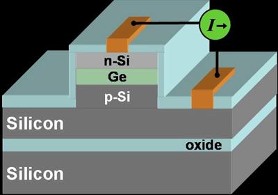


18 Waveguide Photo-detector Design N-Ge i-ge SEM Cross-Section 18
 7.4um x 50um, -2V 4.4um x 100um, -2V 10 8 10 9 10 10 Frequency (Hz) 40 Gb/s Eye Diagram 95% Quantum Efficiency Operating at λ ~1.")
19 SiGe WG PIN - High Speed Performance Relative Responsivity (db) GHz Optical Bandwidth Bandwidth (GHz) um x 50um 4.4um x 100um Voltage (V) 7.4um x 50um, -2V 4.4um x 100um, -2V Frequency (Hz) 40 Gb/s Eye Diagram 95% Quantum Efficiency Operating at λ ~1.56um < 200nA of dark current 19


20 Hybrid Silicon Lasers The Indium Phosphide emits the light into the silicon waveguide The silicon acts as laser cavity: Silicon waveguide routes the light End Facets or gratings are reflectors/mirrors Light bounces back and forth and gets amplified by InP Laser performance determined by InP and Si waveguide - No alignment needed - Multiple lasers with ONE bond - Light inside the waveguide 20
 Wafer Bonding Process (2) III-V Backside Process")
21 Hybrid Laser Fabrication Overview III-V material (unprocessed) is bonded everywhere or only on small parts of a wafer/die Alignment during bonding is not critical III-V is processed after bonding, with mask alignment to underlying silicon markers (1) Wafer Bonding Process (2) III-V Backside Process


22 DBR Lasers on Hybrid Laser Platform Tapers transition from hybrid (active) WG to silicon (passive) WG Gratings in silicon WG form wavelength selective mirrors

23 Hybrid silicon evanescent modal gain Silicon waveguide dimensions control MQW overlap and modal gain Changing waveguide width allows for varying confinement factors within a die or PIC MQW


24 Lithographically defined first order gratings Fabricated using 193-nm laser stepper lithography (HVM compatible) Period Top Down View Grating width Gap length Cross section 0.3um 0.5um 1.5um etch width etch depth


25 Single Wavelength Hybrid Laser grating mirrors in silicon, enabling wavelength-specific laser light output The Device ~1000um Optical Spectrum Line width Measurement ~150 um 25


26 Common Building Block Economy of Scale Integrated SiP Tx and Rx Building Blocks Challenges: - Integrate all building blocks onto Si platforms - Optimize processes for integration (vs. discrete) - Low cost packaging, assembly, and system testing - Do all these using PC-Board techniques and passive optical alignment


27 The 50G Integrated Silicon Photonics Link Transmitting and Receiving Light with Silicon Optical Fiber Integrated Transmitter Chip Integrated Receiver Chip Transmit Module Receiver Module 28


28 Integrated Silicon Photonics Link 4λx12.5 Gb/s Elements are combined together, along with drivers and packaging to form a CWDM link 29


29 Integrated Transmitter Chip Electrical data in Up to 12.5 Gbps/channel Integrates Hybrid Silicon Lasers With Modulators for data encoding and a Multiplexer to put 4 optical channels onto 1 fiber Alignment Pin 50Gbps out on one optical fiber Connector 30 Parallel channels are key to scaling bandwidths at low costs


30 Integrated Receiver Chip Integrates a coupler to receive incoming light with a demultiplexer to split optical signals and Ge-on-Si photodetectors to convert photons to electrons Alignment Pin Coupler Electrical data out Up to12.5 Gbps per channel Gbps in on one optical fiber Connector 31 Receives 4 optical channels at 12.5Gbps and converts to electrical data


")

31 Measured Data 4 hybrid Silicon Laser Outputs 12.5Gbps data output per channel Transmit Receive De-Multiplexer separates wavelengths Electrical Output From Receiver 32 We ran link for more than a day with no errors (>1 Petabit) Translates to Bit-Error-Rate (BER) of < 3e , Intel Corporation. All Rights Reserved

 optical and electrical")
32 4λx10Gbps SiP Tx & Rx Packages Optical Fiber Integrated 4λ x10g SiP Tx Chip Transmitter Package Receiver Package Integrated 4λ x 10G SiGe PD Rx CMOS Driver IC Passive Optical Connector Receiver IC Socketable Edge Connector Tx & Rx packages enable both separable (passive) optical and electrical connectors 33


33 What Could You Download in <1 second? 34

34 What Could You Download in <1 second? 35 1 Tbps could download the entire printed collection of the Library of Congress in about 1½ minutes!


35 The Path to Tera-scale Data Rates Today: 12.5 Gbps x 4 = 50Gbps 25 Gbps x 4 = 100Gbps Scale UP 40G, 100G Scale OUT 12.5 Gbps x 8 = 100Gbps Speed Width Rate 12.5 x4 50G 12.5 x8 100G 25 x16 400G 40 x25 1T Future Terabit+ Links 36 x16, x32 Could enable cost-effective high speed I/O for data-intensive applications
36 CMOS Integration Challenges Film topology Thermal budgets Yield metrology Contaminating the fab Coupling to devices Heat dissipation Complexity Optical wafers must run alongside product, introducing challenges 37
 Transistor on 90nm 8µm Taper 0.25 0.18 0.09 0.9µm Rib 0.5 µm 0.35µm 0.2µm 0.1µm gate 0.3µm Strip 38 Silicon Wafer 38")
37 Example: Topology Depth of focus (DOF) shrinks as litho improves Many optical devices are much taller than transistors New planarization techniques and specific process flows required for advanced litho DOF vs. Litho Technology (µm) Transistor on 90nm 8µm Taper µm Rib 0.5 µm 0.35µm 0.2µm 0.1µm gate 0.3µm Strip 38 Silicon Wafer 38

38 Example: Thermal Budgets 1050 C Temperature Melting Point of InP 1054 C Gate Oxide 950 C S/D Activation Melting Point of Ge 940 C Annealing of Si nc 800 C C Gate Contacts Processing Steps 450 C Thermal budget dictates process step order Cannot use high temperatures at later steps without damage Al / Cu 200 C Packaging Optical Polymers 200 C This determines what can be integrated in the fab vs. backend 39


39 Example: Yield metrology Electronics: CMOS fabs monitor thousands of parameters across wafer in line Tight control e.g. CMOS gate width held to 10 s of angstroms Significant per-wafer cost savings from screening out yield early Screening wafers for early defect detection Integrated vertical coupling approaches Optical In-line wafer level optical probing is very immature Most optical device testing is performed after wafer dicing For HVM, techniques for screening optical wafers must be developed 40
40 Challenges: Optical Integration with CPU Package topside Connection? Monolithic Integration? PROCESSOR FIBERS ORGANIC PACKAGE SOCKET FR4 MOTHERBOARD Board connection? Challenges: Power: CPU s operate with Temperatures near ~85 C Packaging: Compatibility with existing HVM packages connector cost Testing: Testing co-packaged optical /electrical CPU modules Packaging, thermals and testing key to enabling optical in platform 41


41 Summary SiP is a key enabling technology for high BW interconnects Developed first fully integrated Si photonics based Tx & Rx Demonstrated CWDM based Si Photonic 50Gb/s On path to develop fully integrated silicon photonic links to address various interconnect applications 42 Acknowledgements Intel Corp. - SiP team and LAD team Aurrion Inc. For InP processing and hybrid laser developments Micron For Silicon Photonics processing


42 Thank You! 43 To learn more
43 Legal Disclaimer Intel may make changes to specifications and product descriptions at any time, without notice. Performance tests and ratings are measured using specific computer systems and/or components and reflect the approximate performance of Intel products as measured by those tests. Any difference in system hardware or software design or configuration may affect actual performance. Buyers should consult other sources of information to evaluate the performance of systems or components they are considering purchasing. For more information on performance tests and on the performance of Intel products, visit Intel Performance Benchmark Limitations Intel does not control or audit the design or implementation of third party benchmarks or Web sites referenced in this document. Intel encourages all of its customers to visit the referenced Web sites or others where similar performance benchmarks are reported and confirm whether the referenced benchmarks are accurate and reflect performance of systems available for purchase. Intel processor numbers are not a measure of performance. Processor numbers differentiate features within each processor family, not across different processor families. See for details. Intel, processors, chipsets, and desktop boards may contain design defects or errors known as errata, which may cause the product to deviate from published specifications. Current characterized errata are available on request. Intel Virtualization Technology requires a computer system with a processor, chipset, BIOS, virtual machine monitor (VMM) and applications enabled for virtualization technology. Functionality, performance or other virtualization technology benefits will vary depending on hardware and software configurations. Virtualization technology-enabled BIOS and VMM applications are currently in development. Intel Turbo Boost Technology requires a Platform with a processor with Intel Turbo Boost Technology capability. Intel Turbo Boost Technology performance varies depending on hardware, software and overall system configuration. Check with your platform manufacturer on whether your system delivers Intel Turbo Boost Technology. For more information, see No computer system can provide absolute security under all conditions. Intel Trusted Execution Technology (Intel TXT) is a security technology under development by Intel and requires for operation a computer system with Intel Virtualization Technology, a Intel Trusted Execution Technology-enabled Intel processor, chipset, BIOS, Authenticated Code Modules, and an Intel or other Intel Trusted Execution Technology compatible measured virtual machine monitor. In addition, Intel Trusted Execution Technology requires the system to contain a TPMv1.2 as defined by the Trusted Computing Group and specific software for some uses. 64-bit computing on Intel architecture requires a computer system with a processor, chipset, BIOS, operating system, device drivers and applications enabled for Intel 64 architecture. Performance will vary depending on your hardware and software configurations. Consult with your system vendor for more information. Intel, Intel Xeon, Intel Core microarchitecture, and the Intel logo are trademarks or registered trademarks of Intel Corporation or its subsidiaries in the United States and other countries. * Other names and brands may be claimed as the property of others Standard Performance Evaluation Corporation (SPEC) logo is reprinted with permission


44 Silicon Photonics Future Filter ECL Drivers Modulator Multiple Channels CMOS Circuitry TIA TIA Passive Alignment Photodetector 45
Intel: Driving the Future of IT Technologies. Kevin C. Kahn Senior Fellow, Intel Labs Intel Corporation
 Research @ Intel: Driving the Future of IT Technologies Kevin C. Kahn Senior Fellow, Intel Labs Intel Corporation kp Intel Labs Mission To fuel Intel s growth, we deliver breakthrough technologies that
Trickle Up: Photonics and the Future of Computing Justin Rattner Chief Technology Officer Intel Corporation
 Trickle Up: Photonics and the Future of Computing Justin Rattner Chief Technology Officer Intel Corporation * Other names, logos and brands may be claimed as the property of others. Copyright 2009, Intel
Intel Silicon Photonics: from Research to Product
 IEEE Components, Packaging and Manufacturing Technology Chapter, Santa Clara Valley 3/8/2017 Intel Silicon Photonics: from Research to Product MARCH 8, 2017 Ling Liao Principal Engineer Silicon Photonics
Cloud Transformation: Data center usage models driving Cloud computing innovation. Jake Smith, Advanced Server Technologies Data Center Group Intel
 Cloud Transformation: Data center usage models driving Cloud computing innovation. Jake Smith, Advanced Server Technologies Data Center Group Intel Legal Disclaimer Intel may make changes to specifications
Scaling the Compute and High Speed Networking Needs of the Data Center with Silicon Photonics ECOC 2017
 Scaling the Compute and High Speed Networking Needs of the Data Center with Silicon Photonics ECOC 2017 September 19, 2017 Robert Blum Director, Strategic Marketing and Business Development 1 Data Center
Kotura Analysis: WDM PICs improve cost over LR4
 Kotura Analysis: WDM PICs improve cost over LR4 IEEE P802.3bm - 40 Gb/s & 100 Gb/s Fiber Optic Task Force Sept 2012 Contributors: Mehdi Asghari, Kotura Samir Desai, Kotura Arlon Martin, Kotura Recall the
AIM Photonics: Manufacturing Challenges for Photonic Integrated Circuits
 AIM Photonics: Manufacturing Challenges for Photonic Integrated Circuits November 16, 2017 Michael Liehr Industry Driving Force EXA FLOP SCALE SYSTEM Blades SiPh Interconnect Network Memory Stack HP HyperX
Technology challenges and trends over the next decade (A look through a 2030 crystal ball) Al Gara Intel Fellow & Chief HPC System Architect
 Al Gara Intel Fellow & Chief HPC System Architect") Technology challenges and trends over the next decade (A look through a 2030 crystal ball) Al Gara Intel Fellow & Chief HPC System Architect Today s Focus Areas For Discussion Will look at various technologies
Technology challenges and trends over the next decade (A look through a 2030 crystal ball) Al Gara Intel Fellow & Chief HPC System Architect Today s Focus Areas For Discussion Will look at various technologies
Jason Waxman General Manager High Density Compute Division Data Center Group
 Jason Waxman General Manager High Density Compute Division Data Center Group Today 2015 More Users Only 25% of the world is Internet connected today 1 New technologies will connect over 1 billion additional
Organics in Photonics: Opportunities & Challenges. Louay Eldada DuPont Photonics Technologies
 Organics in Photonics: Opportunities & Challenges Louay Eldada DuPont Photonics Technologies Market Drivers for Organic Photonics Telecom Application Product Examples Requirements What Organics Offer Dynamic
MARKET PERSPECTIVE: SEMICONDUCTOR TREND OF 2.5D/3D IC WITH OPTICAL INTERFACES PHILIPPE ABSIL, IMEC
 MARKET PERSPECTIVE: SEMICONDUCTOR TREND OF 2.5D/3D IC WITH OPTICAL INTERFACES PHILIPPE ABSIL, IMEC OUTLINE Market Trends & Technology Needs Silicon Photonics Technology Remaining Key Challenges Conclusion
PLANAR LIGHTWAVE CIRCUITS FOR USE IN ADVANCED OPTICAL INSTRUMENTATION
 PLANAR LIGHTWAVE CIRCUITS FOR USE IN ADVANCED OPTICAL INSTRUMENTATION AN ENABLENCE ARTICLE WRITTEN BY DR. MATT PEARSON, VP TECHNOLOGY & ASHOK BALAKRISHNAN, DIRECTOR OF PRODUCT DEVELOPMENT PUBLISHED IN
Photonics Integration in Si P Platform May 27 th Fiber to the Chip
 Photonics Integration in Si P Platform May 27 th 2014 Fiber to the Chip Overview Introduction & Goal of Silicon Photonics Silicon Photonics Technology Wafer Level Optical Test Integration with Electronics
Interconnect Challenges in a Many Core Compute Environment. Jerry Bautista, PhD Gen Mgr, New Business Initiatives Intel, Tech and Manuf Grp
 Interconnect Challenges in a Many Core Compute Environment Jerry Bautista, PhD Gen Mgr, New Business Initiatives Intel, Tech and Manuf Grp Agenda Microprocessor general trends Implications Tradeoffs Summary
Optical Interconnects: Trend and Applications
 Optical Interconnects: Trend and Applications Yi-Jen Chan EOL, ITRI Wireless & Optical Communications conference 2008 April 23, 2008 OUTLINE Background and Motivation Trends of Optical Interconnects Technology
Risk Factors. Rev. 4/19/11
 Risk Factors Today s presentations contain forward-looking statements. All statements made that are not historical facts are subject to a number of risks and uncertainties, and actual results may differ
PSMC Roadmap For Integrated Photonics Manufacturing
 PSMC Roadmap For Integrated Photonics Manufacturing Richard Otte Promex Industries Inc. Santa Clara California For the Photonics Systems Manufacturing Consortium April 21, 2016 Meeting the Grand Challenges
Silicon Based Packaging for 400/800/1600 Gb/s Optical Interconnects
 Silicon Based Packaging for 400/800/1600 Gb/s Optical Interconnects The Low Cost Solution for Parallel Optical Interconnects Into the Terabit per Second Age Executive Summary White Paper PhotonX Networks
Luxtera PN Silicon CMOS Photonic Chip Freescale 130 nm SOI CMOS Process
 Luxtera PN1000001 Silicon CMOS Photonic Chip Process Review 1891 Robertson Road, Suite 500, Ottawa, ON K2H 5B7 Canada Tel: 613-829-0414 www.chipworks.com Process Review Some of the information in this
Accelerating HPC. (Nash) Dr. Avinash Palaniswamy High Performance Computing Data Center Group Marketing
 Dr. Avinash Palaniswamy High Performance Computing Data Center Group Marketing") Accelerating HPC (Nash) Dr. Avinash Palaniswamy High Performance Computing Data Center Group Marketing SAAHPC, Knoxville, July 13, 2010 Legal Disclaimer Intel may make changes to specifications and product
Accelerating HPC (Nash) Dr. Avinash Palaniswamy High Performance Computing Data Center Group Marketing SAAHPC, Knoxville, July 13, 2010 Legal Disclaimer Intel may make changes to specifications and product
Silicon Photonics PDK Development
 Hewlett Packard Labs Silicon Photonics PDK Development M. Ashkan Seyedi Large-Scale Integrated Photonics Hewlett Packard Labs, Palo Alto, CA ashkan.seyedi@hpe.com Outline Motivation of Silicon Photonics
Heterogeneous Integration and the Photonics Packaging Roadmap
 Heterogeneous Integration and the Photonics Packaging Roadmap Presented by W. R. Bottoms Packaging Photonics for Speed & Bandwidth The Functions Of A Package Protect the contents from damage Mechanical
Moore s s Law, 40 years and Counting
 Moore s s Law, 40 years and Counting Future Directions of Silicon and Packaging Bill Holt General Manager Technology and Manufacturing Group Intel Corporation InterPACK 05 2005 Heat Transfer Conference
Multi-Core Microprocessor Chips: Motivation & Challenges
 Multi-Core Microprocessor Chips: Motivation & Challenges Dileep Bhandarkar, Ph. D. Architect at Large DEG Architecture & Planning Digital Enterprise Group Intel Corporation October 2005 Copyright 2005
SOI at the heart of the silicon photonics design. Arnaud Rigny, Business Development Manager Semicon Europa, TechArena
 SOI at the heart of the silicon photonics design Arnaud Rigny, Business Development Manager Semicon Europa, TechArena Outline 1 Market demand for optical interconnect 2 Silicon on Insulator for optical
SILICON PHOTONICS WAVEGUIDE AND ITS FIBER INTERCONNECT TECHNOLOGY. Jeong Hwan Song
 SILICON PHOTONICS WAVEGUIDE AND ITS FIBER INTERCONNECT TECHNOLOGY Jeong Hwan Song CONTENTS Introduction of light waveguides Principals Types / materials Si photonics Interface design between optical fiber
Packaging and Integration Technologies for Silicon Photonics. Dr. Peter O Brien, Tyndall National Institute, Ireland.
 Packaging and Integration Technologies for Silicon Photonics Dr. Peter O Brien, Tyndall National Institute, Ireland. Opportunities for Silicon Photonics Stress Sensors Active Optical Cable 300 mm Silicon
The MIT Communications Technology Roadmap Program IPI TWG Report
 The MIT Communications Technology Roadmap Program IPI TWG Report May 19, 2006 Louay Eldada Integration, Packaging & Interconnection Technology Working Group CTO, VP Engineering DuPont Photonics Chair,
Enhancing Analysis-Based Design with Quad-Core Intel Xeon Processor-Based Workstations
 Performance Brief Quad-Core Workstation Enhancing Analysis-Based Design with Quad-Core Intel Xeon Processor-Based Workstations With eight cores and up to 80 GFLOPS of peak performance at your fingertips,
Xilinx SSI Technology Concept to Silicon Development Overview
 Xilinx SSI Technology Concept to Silicon Development Overview Shankar Lakka Aug 27 th, 2012 Agenda Economic Drivers and Technical Challenges Xilinx SSI Technology, Power, Performance SSI Development Overview
Introduction to Integrated Photonic Devices
 Introduction to Integrated Photonic Devices Class: Integrated Photonic Devices Time: Wed. 1:10pm ~ 3:00pm. Fri. 10:10am ~ 11:00am Classroom: 資電 106 Lecturer: Prof. 李明昌 (Ming-Chang Lee) Block Diagram of
Applications for Mapper technology Bert Jan Kampherbeek
 Applications for Mapper technology Bert Jan Kampherbeek Co-founder & CEO Today s agenda Mapper technology Principles of operation Development status and performance Specification summary Mapper applications
PIC design across platforms. Ronald Broeke Bright Photonics
 PIC design across platforms Ronald Broeke Bright Photonics OUTLINE Introduction PIC applications & designs MPW Materials & platforms Design modules PICs in Phoxtrot Design House for Photonics ICs Custom
2009 International Solid-State Circuits Conference Intel Paper Highlights
 2009 International Solid-State Circuits Conference Intel Paper Highlights Mark Bohr Intel Senior Fellow Soumyanath Krishnamurthy Intel Fellow 1 2009 ISSCC Intel Paper Summary Under embargo until February,
Active Optical Cables. Dr. Stan Swirhun VP & GM, Optical Communications April 2008
 Active Optical Cables Dr. Stan Swirhun VP & GM, Optical Communications April 2008 Supplier of Mixed Signal Products Supplier of Mixed Signal Communication Semiconductors, public $230M Medical Communications
Introduction. Summary. Why computer architecture? Technology trends Cost issues
 Introduction 1 Summary Why computer architecture? Technology trends Cost issues 2 1 Computer architecture? Computer Architecture refers to the attributes of a system visible to a programmer (that have
From Majorca with love
 From Majorca with love IEEE Photonics Society - Winter Topicals 2010 Photonics for Routing and Interconnects January 11, 2010 Organizers: H. Dorren (Technical University of Eindhoven) L. Kimerling (MIT)
Developing flexible WDM networks using wavelength tuneable components
 Developing flexible WDM networks using wavelength tuneable components A. Dantcha 1, L.P. Barry 1, J. Murphy 1, T. Mullane 2 and D. McDonald 2 (1) Research Institute for Network and Communications Engineering,
2000 Technology Roadmap Optoelectronics. John Stafford, Motorola January 17, 2001
 2000 Technology Roadmap Optoelectronics John Stafford, Motorola January 17, 2001 Optoelectronic Roadmap Agenda Optoelectronics Market Overview Optical Communications Roadmap Optical Communications Technology
Integrated Optical Devices
 Integrated Optical Devices May 2018 Integrated Optical Devices 2017 a good year for Silicon Photonics, a fantastic year for integrated InP and GaAs optics Source: Luxtera with text added by LightCounting
Moving Forward with the IPI Photonics Roadmap
 Moving Forward with the IPI Photonics Roadmap TWG Chairs: Rich Grzybowski, Corning (acting) Rick Clayton, Clayton Associates Integration, Packaging & Interconnection: How does the chip get to the outside
Scalable Computing Systems with Optically Enabled Data Movement
 Scalable Computing Systems with Optically Enabled Data Movement Keren Bergman Lightwave Research Laboratory, Columbia University Rev PA1 2 Computation to Communications Bound Computing platforms with increased
Stacked Silicon Interconnect Technology (SSIT)
") Stacked Silicon Interconnect Technology (SSIT) Suresh Ramalingam Xilinx Inc. MEPTEC, January 12, 2011 Agenda Background and Motivation Stacked Silicon Interconnect Technology Summary Background and Motivation
Stacked Silicon Interconnect Technology (SSIT) Suresh Ramalingam Xilinx Inc. MEPTEC, January 12, 2011 Agenda Background and Motivation Stacked Silicon Interconnect Technology Summary Background and Motivation
Packaging for parallel optical interconnects with on-chip optical access
 Packaging for parallel optical interconnects with on-chip optical access I. INTRODUCTION Parallel optical interconnects requires the integration of lasers and detectors directly on the CMOS chip. In the
Advancing high performance heterogeneous integration through die stacking
 Advancing high performance heterogeneous integration through die stacking Suresh Ramalingam Senior Director, Advanced Packaging European 3D TSV Summit Jan 22 23, 2013 The First Wave of 3D ICs Perfecting
Intel SSD Data center evolution
 Intel SSD Data center evolution March 2018 1 Intel Technology Innovations Fill the Memory and Storage Gap Performance and Capacity for Every Need Intel 3D NAND Technology Lower cost & higher density Intel
Open access to photonic integration technologies
 Open access to photonic integration technologies Academic and Industrial examples of photonic integrated circuits Katarzyna Ławniczuk k.lawniczuk@tue.nl What is photonic integration technology? multiple
Announcements. Advanced Digital Integrated Circuits. No office hour next Monday. Lecture 2: Scaling Trends
 EE4 - Spring 008 Advanced Digital Integrated Circuits Lecture : Scaling Trends Announcements No office hour next Monday Extra office hours Tuesday and Thursday -3pm CMOS Scaling Rules Voltage, V / α tox/α
Evolving Small Cells. Udayan Mukherjee Senior Principal Engineer and Director (Wireless Infrastructure)
") Evolving Small Cells Udayan Mukherjee Senior Principal Engineer and Director (Wireless Infrastructure) Intelligent Heterogeneous Network Optimum User Experience Fibre-optic Connected Macro Base stations
Evolving Small Cells Udayan Mukherjee Senior Principal Engineer and Director (Wireless Infrastructure) Intelligent Heterogeneous Network Optimum User Experience Fibre-optic Connected Macro Base stations
Fiber Optic Cabling Systems for High Performance Applications
 Fiber Optic Cabling Systems for High Performance Applications BICSI Conference Bangkok, Thailand 17-18 November 2016 Nicholas Yeo, RCDD/NTS/DCDC Data Center Trends Computing evolution Cloud computing Servers
Next Generation Transceivers: The Roadmap Component Driver Contributions from Roadmap team. Dominic O Brien Mike Schabel
 Next Generation Transceivers: The Roadmap Component Driver Contributions from Roadmap team Dominic O Brien Mike Schabel Outline New markets Key challenges Potential evolution Recommendations Fibre to the
RE-IMAGINING THE DATACENTER. Lynn Comp Director of Datacenter Solutions and Technologies
 RE-IMAGINING THE DATACENTER Lynn Comp Director of Datacenter Solutions and Technologies IT: Period of Transformation Computer-Centric Network-Centric Human-Centric Focused on Productivity through automation
1x40 Gbit/s and 4x25 Gbit/s Transmission at 850 nm on Multimode Fiber
 1x40 Gbit/s and 4x25 Gbit/s Transmission at 850 nm on Multimode Fiber, Berlin, Germany J.-R. Kropp, N. Ledentsov, J. Lott, H. Quast Outline 1. Feasibility of components for 4x25G and 1x40G solutions for
Monolithic 3D Integration using Standard Fab & Standard Transistors. Zvi Or-Bach CEO MonolithIC 3D Inc.
 Monolithic 3D Integration using Standard Fab & Standard Transistors Zvi Or-Bach CEO MonolithIC 3D Inc. 3D Integration Through Silicon Via ( TSV ), Monolithic Increase integration Reduce interconnect total
Moore s Law: Alive and Well. Mark Bohr Intel Senior Fellow
 Moore s Law: Alive and Well Mark Bohr Intel Senior Fellow Intel Scaling Trend 10 10000 1 1000 Micron 0.1 100 nm 0.01 22 nm 14 nm 10 nm 10 0.001 1 1970 1980 1990 2000 2010 2020 2030 Intel Scaling Trend
High Versatility High Throughput Functional Testing. Robert Polster, David Calhoun, Keren Bergman
 High Versatility High Throughput Functional Testing Robert Polster, David Calhoun, Keren Bergman Challenges of High-Throughput Functional Testing for Scalable Manufacturing Numerous Functional Applications
New generation integrated photonic systems-on-chip enabling Tb/scapacity
 New generation integrated photonic systems-on-chip enabling Tb/scapacity Photonic Routers (Invited) Leontios Stampoulidis, Efstratios Kehayas, Panagiotis Zakynthinos, Dimitrios Apostolopoulos, Dimitrios
Intel Xeon Processor E v3 Family
 Intel Xeon Processor E5-2600 v3 Family October 2014 Document Number: 331309-001US All information provided here is subject to change without notice. Contact your Intel representative to obtain the latest
Announcements. Advanced Digital Integrated Circuits. No office hour next Monday. Lecture 2: Scaling Trends
 EE24 - Spring 2008 Advanced Digital Integrated Circuits Lecture 2: Scaling Trends Announcements No office hour next Monday Extra office hours Tuesday and Thursday 2-3pm 2 CMOS Scaling Rules Voltage, V
High Performance Computing The Essential Tool for a Knowledge Economy
 High Performance Computing The Essential Tool for a Knowledge Economy Rajeeb Hazra Vice President & General Manager Technical Computing Group Datacenter & Connected Systems Group July 22 nd 2013 1 What
Hybrid On-chip Data Networks. Gilbert Hendry Keren Bergman. Lightwave Research Lab. Columbia University
 Hybrid On-chip Data Networks Gilbert Hendry Keren Bergman Lightwave Research Lab Columbia University Chip-Scale Interconnection Networks Chip multi-processors create need for high performance interconnects
VCSEL-based solderable optical modules
 4th Symposium on Optical Interconnect for Data Centres VCSEL-based solderable optical modules Hideyuki Nasu FITEL Products Division Furukawa Electric Co., Ltd. H. Nasu/ FITEL Products Division, Furukawa
Extending Energy Efficiency. From Silicon To The Platform. And Beyond Raj Hazra. Director, Systems Technology Lab
 Extending Energy Efficiency From Silicon To The Platform And Beyond Raj Hazra Director, Systems Technology Lab 1 Agenda Defining Terms Why Platform Energy Efficiency Value Intel Research Call to Action
FCI-XXXA Large Active Area 970nm Si Monitor Photodiodes
 FCI-XXXA Large Active Area 970nm Si Monitor Photodiodes FCI-020A and FCI-040A with active area sizes of 0.5mm and 1.0mm, are parts of OSI Optoelectronics s large active area IR sensitive Silicon detectors
UBCx Phot1x: Silicon Photonics Design, Fabrication and Data Analysis
 UBCx Phot1x: Silicon Photonics Design, Fabrication and Data Analysis Course Syllabus Table of Contents Course Syllabus 1 Course Overview 1 Course Learning Objective 1 Course Philosophy 1 Course Details
Silicon Photonics System Integration by Ultra High Precision Photonic Packaging Techniques
 Silicon Photonics System Integration by Ultra High Precision Photonic Packaging Techniques Dr. Henning Schröder, Fraunhofer IZM Dr. Henning Schröder Fraunhofer IZM, Berlin fon: ++49 30 46403-277, fax:
Re-Architecting Cloud Storage with Intel 3D XPoint Technology and Intel 3D NAND SSDs
 Re-Architecting Cloud Storage with Intel 3D XPoint Technology and Intel 3D NAND SSDs Jack Zhang yuan.zhang@intel.com, Cloud & Enterprise Storage Architect Santa Clara, CA 1 Agenda Memory Storage Hierarchy
Intel Workstation Platforms
 Product Brief Intel Workstation Platforms Intel Workstation Platforms For intelligent performance, automated Workstations based on the new Intel Microarchitecture, codenamed Nehalem, are designed giving
Core. for Embedded Computing. Processors T9400, P8400, SL9400, SL9380, SP9300, SU9300, T7500, T7400, L7500, L7400 and U7500.
 Intel Core 2 Duo Processors Embedded Computing Intel Core 2 Duo Processors for Embedded Computing Processors T9400, P8400, SL9400, SL9380, SP9300, SU9300, T7500, T7400, L7500, L7400 and U7500 Product Overview
Mm-wave integrated waveguide components in silicon technology
 Mm-wave integrated waveguide components in silicon technology G. Gentile, M. Spirito, L.C.N. de Vreede, et al. Electronics Research Laboratory (ELCA), Dimes, Delft University of Technology, The Netherlands
Product Data Sheet. 3M Active Optical Cable (AOC) Assemblies for CX4 and QSFP+ Applications
 Assemblies for CX4 and QSFP+ Applications") 78-5102-0126-8 B Product Data Sheet 3M Active Optical Cable (AOC) Assemblies for CX4 and QSFP+ Supersedes: Rev A Page: 1 of 9 Table of Contents 1.0 DESCRIPTION...2 2.0 AOC BLOCK DIAGRAM...2 3.0 CONNECTOR
78-5102-0126-8 B Product Data Sheet 3M Active Optical Cable (AOC) Assemblies for CX4 and QSFP+ Supersedes: Rev A Page: 1 of 9 Table of Contents 1.0 DESCRIPTION...2 2.0 AOC BLOCK DIAGRAM...2 3.0 CONNECTOR
Integrated Micro and Nano Photonic Systems for Peta scale Networking
 Integrated Micro and Nano Photonic Systems for Peta scale Networking Prof. S. J. Ben Yoo, UC Davis Campus CITRIS Director yoo@ece.ucdavis.edu http://sierra.ece.ucdavis.edu http://citris.ucdavis.edu Tokyo,
Signature Core Fiber Optic Cabling System
 White Paper June 2012 WP-17 Signature Core Fiber Optic Cabling System Multimode Fiber: Understanding Chromatic Dispersion Introduction The performance and reliability of networks within the Data Center
CMOSETR Session C1, July 7 (Macroelectronics)
") Universal Flexible Hybrid System Development Kit including MCU, ADC and RFIC Prepared for: CMOSETR Session C1, July 7 (Macroelectronics) Doug Hackler President & CEO doughackler@americansemi.com 208 336-2773
Universal Flexible Hybrid System Development Kit including MCU, ADC and RFIC Prepared for: CMOSETR Session C1, July 7 (Macroelectronics) Doug Hackler President & CEO doughackler@americansemi.com 208 336-2773
Intra Optical Data Center Interconnection Session 2: Debating Intra-DC solutions and Photonic Integration approaches
 Intra Optical Data Center Interconnection Session 2: Debating Intra-DC solutions and Photonic Integration approaches Co-Organizer/Presider/Session Chair: Dr. Ioannis Tomkos Networks and Optical Communications
Technology Platform Segmentation
 HOW TECHNOLOGY R&D LEADERSHIP BRINGS A COMPETITIVE ADVANTAGE FOR MULTIMEDIA CONVERGENCE Technology Platform Segmentation HP LP 2 1 Technology Platform KPIs Performance Design simplicity Power leakage Cost
Brief Background in Fiber Optics
 The Future of Photonics in Upcoming Processors ECE 4750 Fall 08 Brief Background in Fiber Optics Light can travel down an optical fiber if it is completely confined Determined by Snells Law Various modes
D5.2: Packaging and fiber-pigtailing of the 2 nd generation 2x2 optical interconnect router
 ICT - Information and Communication Technologies Merging Plasmonics and Silicon Photonics Technology towards Tb/s routing in optical interconnects Collaborative Project Grant Agreement Number 249135 D5.2:
400G PAM4 The Wave of the Future. Michael G. Furlong - Senior Director, Product Marketing
 400G The Wave of the Future Michael G. Furlong - Senior Director, Product Marketing mfurlong@inphi.com ECOC 2017 100G is Ramping in the Cloud 100G Now Shipping (~2H2016) Numerous Market Reports Millions
EUV Lithography and Overlay Control
 YMS Magazine DECEMBER 2017 EUV Lithography and Overlay Control Efi Megged, Mark Wylie and Cathy Perry-Sullivan L A-Tencor Corporation One of the key parameters in IC fabrication is overlay the accuracy
Beykent University Network Courses
 /8/24 Beykent University Network Courses Module 3 : Optical Networks and Systems Part kaanavsarasan.weebly.com November 24 November 24 Course Outline Introduction to Optics Components of Optical Networks
1-Fiber Detachable DVI module, DVFX-100
 1-Fiber Detachable DVI module, DVFX-100 DATA SHEET Contents Description Features Applications Technical Specifications Functions Drawing Fiber Connection DVI Pin Description Revision History OPTICIS HQ
1-Fiber Detachable DVI module, DVFX-110
 1-Fiber Detachable DVI module, DVFX-110 DATA SHEET Contents Description Features Applications Technical Specifications Functions Drawing Fiber Connection DVI Pin Description OPTICIS HQ Opticis Co., Ltd.
Jeff Kash, Dan Kuchta, Fuad Doany, Clint Schow, Frank Libsch, Russell Budd, Yoichi Taira, Shigeru Nakagawa, Bert Offrein, Marc Taubenblatt
 IBM Research PCB Overview Jeff Kash, Dan Kuchta, Fuad Doany, Clint Schow, Frank Libsch, Russell Budd, Yoichi Taira, Shigeru Nakagawa, Bert Offrein, Marc Taubenblatt November, 2009 November, 2009 2009 IBM
Expand Your HPC Market Reach and Grow Your Sales with Intel Cluster Ready
 Intel Cluster Ready Expand Your HPC Market Reach and Grow Your Sales with Intel Cluster Ready Legal Disclaimer Intel may make changes to specifications and product descriptions at any time, without notice.
Presented by : Sadegh Riyahi Majid Shokrolahi
 Politecnico di Milano Polo Regionale di Como Architectures for multimedia systems Professor : Cristina Silvano Presented by : Sadegh Riyahi Majid Shokrolahi 29th June 2010 Outline Introduction What is
Photon-to-Photon CMOS Imager: Opto-Electronic 3D Integration
 Photon-to-Photon CMOS Imager: Opto-Electronic 3D Integration Outline Key technologies for future CMOS imagers Bottlenecks for high speed imaging Our proposal Take home message Oct 12, 2017 Photon-to-Photon
WDM-PON Architecture Implement Using AWG with Multicasting Efficiency
 WDMPON Architecture Implement Using AWG with Multicasting Efficiency Nerkar Narendra N, Kadu Mahesh B Electronics and Telecommunication Department, AVCOE Sangamner, India. ABSTRACT: We present the experimental
Intel High-Performance Computing. Technologies for Engineering
 6. LS-DYNA Anwenderforum, Frankenthal 2007 Keynote-Vorträge II Intel High-Performance Computing Technologies for Engineering H. Cornelius Intel GmbH A - II - 29 Keynote-Vorträge II 6. LS-DYNA Anwenderforum,
AUTOFOCUS SENSORS & MICROSCOPY AUTOMATION IR LASER SCANNING CONFOCAL MICROSCOPE IRLC DEEP SEE. Now See Deeper than ever before
 AUTOFOCUS SENSORS & MICROSCOPY AUTOMATION IR LASER SCANNING CONFOCAL MICROSCOPE IRLC DEEP SEE Now See Deeper than ever before Review and inspection of non visible subsurface defects Non visible and subsurface
Microelettronica. J. M. Rabaey, "Digital integrated circuits: a design perspective" EE141 Microelettronica
 Microelettronica J. M. Rabaey, "Digital integrated circuits: a design perspective" Introduction Why is designing digital ICs different today than it was before? Will it change in future? The First Computer
Photonics & 3D, Convergence Towards a New Market Segment Eric Mounier Thibault Buisson IRT Nanoelec, Grenoble, 21 mars 2016
 From Technologies to Market Photonics & 3D, Convergence Towards a New Market Segment Eric Mounier Thibault Buisson IRT Nanoelec, Grenoble, 21 mars 2016 2016 CONTENT Silicon Photonics value proposition
Integrated Optical Devices
 Integrated Optical Devices January 2017 Month 2015 Integrated Optical Devices Is Silicon Photonics a Disruptive Technology? Source: Luxtera with text added by LightCounting 7 Table of Contents Table of
Next Generation Requirements for DWDM network
 Next Generation Requirements for DWDM network Roman Egorov Verizon Laboratories May 3, 2011 Verizon copyright 2011. NG Requirements for DWDM network: Outline Optical Transport Network Metro vs. Long-Haul
6th Generation Intel Core Processor Series
 6th Generation Intel Core Processor Series Application Power Guidelines Addendum Supporting the 6th Generation Intel Core Processor Series Based on the S-Processor Lines August 2015 Document Number: 332854-001US
ECE520 VLSI Design. Lecture 1: Introduction to VLSI Technology. Payman Zarkesh-Ha
 ECE520 VLSI Design Lecture 1: Introduction to VLSI Technology Payman Zarkesh-Ha Office: ECE Bldg. 230B Office hours: Wednesday 2:00-3:00PM or by appointment E-mail: pzarkesh@unm.edu Slide: 1 Course Objectives
Silicon Photonics: Failing to Deliver on WDM Promises for the Datacenter
 Silicon Photonics: Failing to Deliver on WDM Promises for the Datacenter Silicon Photonics: Is it still in hype or on its way to the field? OFC 2015 Workshop 22 March 2015 Chris Cole Mainstream Datacenter
Ubiquitous Location: challenges and opportunities of enabling all-day, everywhere location for all mobile platforms
 Ubiquitous Location: challenges and opportunities of enabling all-day, everywhere location for all mobile platforms CSNC, Nanjing May 22, 2014 Greg Turetzky 1 Copyright 2014 Intel Corporation. All rights
Intel s Architecture for NFV
 Intel s Architecture for NFV Evolution from specialized technology to mainstream programming Net Futures 2015 Network applications Legal Disclaimer INFORMATION IN THIS DOCUMENT IS PROVIDED IN CONNECTION
Instruction Manual RT-91685SL RR-91685SL Sixteen Channel Video Multiplexer With Two Bi-directional Data Channels
 Instruction Manual RT-91685SL RR-91685SL Sixteen Channel Video Multiplexer With Two Bi-directional Data Channels Copyright 2007, American Fibertek, Inc. 0501JD Table of Contents Functional Description...3