Scalable Computing Systems with Optically Enabled Data Movement
|
|
|
- Lindsay Ross
- 5 years ago
- Views:
Transcription


1


2 Scalable Computing Systems with Optically Enabled Data Movement Keren Bergman Lightwave Research Laboratory, Columbia University Rev PA1 2


3 Computation to Communications Bound Computing platforms with increased parallelism at all scales: Sun Niagara 8 cores 2005 Sony/Toshiba/IBM Cell 9 cores 2006 Intel Polaris 80 cores 2007 Tilera TILE-Gx cores 2009 NVIDIA Fermi 512 cores 2012 Handheld System-on-Chip Embedded Systems Data Centers COLUMBIA UNIVERSITY 3
4 Data Movement Dominates- Energy John Shalf, LBL
5 Data movement bandwidth taper challenge Paul Franzon, NCSU Bandwidth taper for conventional electronic interconnect reduces by: 2 orders of magnitude as data propagates from the chip, across the die and the system racks
6 Photonic Interconnects for Computing Platforms: Change the Rules for Bandwidth per Watt TX RX TX RX TX RX TX RX TX RX TX RX PHOTONICS Modulate/receive data stream once per communication event Wavelength Parallelism : Broadband switch routes entire multi wavelength stream High I/O bandwidth density Distance Independence Off chip BW on chip BW for nearly same power ELECTRONICS Buffer, receive, and re transmit at every repeater/router Space Parallelism : Each bus lane routed independently (P N LANES ) Low I/O bandwidth density Off chip BW requires much more power than on chip BW In the context of computing Photonic communication can be fully exploited only by rethinking how to leverage its unique datamovement capabilities to realize new system architectures

7 Photonic Interconnectivity delivers scalability energy and bandwidth density


8 Silicon Photonics Silicon-on-insulator (SOI) platform photonic building blocks: High index contrast enables high confinement, low-loss propagation, virtually lossless bending MIT Sandia Ghent Luxtera IBM Intel Cornell Cornell/Columbia Columbia COLUMBIA UNIVERSITY 8

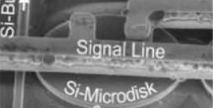
9 Silicon Photonic Interconnects in Computing Silicon photonics: Off chip BW = On chip BW for nearly same power. Dense WDM = extreme bandwidth density I/O bottlenecks Broadband switch routes entire multi wavelength stream. Bandwidth density: ~ 2 Tbps/20 m pitch at chip s edge. 9 [F. Doany et al., JLT 29 (4) (2011)]


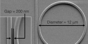
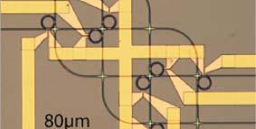
10 Silicon Photonics Optical Interconnection Networks -Silicon as core material High refractive index and high contrast sub micron cross section dimensions, smallest bend radius. -Small footprint devices 10 μm 1 mm scale compared to cm level scale for telecom components -Low power consumption Can reach <1 pj/bit per full point to point link -Aggressive WDM platform Bandwidth densities 1 2Tb/s per pin -Silicon wafer level CMOS processing Integration Mass production, price Compatibility with CMOS fabs, CMOS electronics Silicon Microring/Microdisk Based Devices Switching (Cornell/Columbia) Modulation (Oracle) WDM Modulation & Demultiplexing 10
. OOK modulator can be based on small resonance shifts.")
, WDM mux / demux, filters.")
11 Active / Tunable Micoring Devices P/N-doping of silicon - diodes for carrier injection (p-i-n) or depletion (p-n). OOK modulator can be based on small resonance shifts. Power dissipation device volume fj/bit. Integrated local heaters allow thermal stabilization. Functionalities: modulators (up to 40 Gbps), WDM mux / demux, filters. Blue shift p-i-n Operating Wavelength 11 [16]

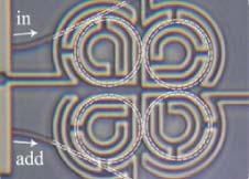
12 Microring Based Comm. Links Wavelength selectivity inherently supports WDM configuration with a single bus waveguide. R R+ΔR R+2ΔR R+3ΔR Analytical Model 12


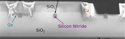
13 Dense WDM Microring Link Design Design driven by best possible single-waveguide optical link in terms of BW density and energy efficiency Laser Array Optical Die Optical Die Laser Array Tx Array: Si or SiN bus WG Inverse-taper edge couplers Depletion-mode microring modulators SM fiber: PM Negligible loss up to 1 km Rx Array: Thermally tuned microring filters Ge PD on drop ports 13
14 Analysis of a Microring-Based Optical I/O Link Approach: Account for all mechanisms involved in power penalty and loss Analyze expected performance and scalability of microring-based SiPh links Identify key parameters / devices that need further improvement. Identify design trade-offs and optimal work points for the link. Rev PA1 14


15 Optical Power Budget Required Input Laser Power Per Channel (dbm) Power Limit 12.5-Gbps Channels 25-Gbps Channels 70 channels, 1.75 Tb/s 152 channels, 1.9 Tb/s WDM Channel Spacing (GHz) 15 Power per channel inversely proportional to channel spacing. 20 dbm power limit determines achievable BW Gb/s test case more scalable. Mainly because of receiver sensitivity.
16 Link Power Efficiency Examine for a 1.55-Tb/s aggregate BW work point: Gb/s rate, 50-GHz spacing, 124 channels Gb/s rate, 100-GHz spacing, 62 channels Gb/s Modulation 25-Gb/s Modulation Microring modulation 0.01 pj/bit 0.01 pj/bit Modulation driver 0.1 pj/bit 0.3 pj/bit Modulator thermal stabilization 0.11 pj/bit 0.06 pj/bit Demux thermal stabilization 0.11 pj/bit 0.06 pj/bit PD and receiver circuitry 0.4 pj/bit 1 pj/bit Laser source 5.56 efficiency 7 efficiency (wall-plug efficiency) 0.56 efficiency 0.7 efficiency Electronic data transmission to and from 1 pj/bit 2 pj/bit optical module Overall with 10% laser wall-plug efficiency 2.3 pj/b 4.1 pj/b Rev PA1 16


17 Path to Commercialization: Silicon Photonic Technology Fundamental Discoveries Introduction of Innovative Devices and Processes Integration and Commercialization low loss, single mode waveguiding high speed microring modulators and switches arrayed waveguide gratings Hybrid platforms Monolithic CMOS Integration optical coupling optical modulation via carrier injection Germanium photodetectors ultra low loss waveguides and crossings hybrid silicon lasers Transceivers for Datacom Foundry Services 1990s 2000s

18 Columbia LRL Demonstrations 320 Gb/s WDM transmitters based on silicon microrings 8 channel WDM transmitter based on conventional common bus architecture 32fJ/bit modulation power efficiency, less than 0.04 mm 2 chip area highest aggregated data rate achieved in silicon transmitters 8-ring transmitter spectra 40Gb/s eye diagrams Rev PA1 18


19 Silicon Photonics for Exascale Computing DRAM Su pe rc om pu tin g Exaflop-scale high-performance computing system CMPs 3DI Stack Silicon Photonic Interconnection Network bl ad es wi th pr oc es so Seamless hierarchical rb photonic cross-layer oa rd communication to the chip s, s P Photonic Memory Stack interconnects CM d th an support inter-rack i w, oc k y N communications in r c o CMPs ta m nic s current HPCS e to I 3D m ho p

20 Silicon Photonics based systems design Photonic Network-on-Chip Design Keren Bergman, Luca Carloni, Aleksandr Biberman, Johnnie Chan, and Gilbert Hendry Series: Integrated Circuits and Systems, Vol. 68, Springer Science + Business Media New York 2014 Rev PA1 20


21 Photonic Enabled Systems: Multi Level Co Design PhoenixSim: Design, Modeling and Simulation Environment Physical link layer: SiP components modeling Link bandwidth maximization Optical power budget validation Network layer Optical data flow, switching, routing protocols Network performance analysis Application layer BW and data flow application mapping Optically enabled algorithm re-design Large scale application simulation


22 PhoenixSim Suite From a general data-center description Network structure level: Javanco Topology construction and visualization, data-structures for other tools System-level physical layer modeling: PILOT Study of individual component impact on the signal Component parameter optimization for higher bandwidth Response to traffic and application demands: LWSim Packets/connection dynamics, protocols, queues, contention Computing nodes N N N S S S B B B Backbone routers Persistent storage PhoenixSim suite Signal quality analysis Scaling analysis Bandwidth Latency est. Lab measurements Models found in literature PILOT Javanco LWSim Timing estimation Application models Projections Traffic models Interconnect design Ad hoc simulations Rev PA1 22


23 Connecting with the Applications Original network and algorithm Various opportunities to leverage optics: 4x bandwidth model -39% More bandwidth With more wavelengths and higher rates Flattened bandwidth model -14% More concurrency Thanks to distanceindependent links Interleaved communication and computation algorithm -52% More agility With all-optical processing Interleaving


24 Co-design an example 1. Replace central switch architecture by distributed network 2. Make the application topology aware Measured traffic (by simulation) for unaware application Measured traffic (by simulation) for a topology aware application 8 nodes per cluster 16 nodes per cluster 32 nodes per cluster Rev PA1 24


25 Co-design initial simulation results nearly the same speed-up is achieved as with ideal central switch Using smaller radixes and with a non full bisectional bandwidth Central controlled high radix switch Adapted distributed architecture with small radix switches Rev PA1 25
26 Putting it all together FPGA Programmable SiP Interconnected Networking Platform Rev PA1 26
27 FPGA Controlled Silicon Photonic Interconnected System Optical Network Interface: O-NIC Link Negotiation and Subsystem Control 1: Link Negotiation M M M O SiP O O D D D WDM TX Source FPGA node TX Dest. FPGA node RX RX Electronics SiP WDM Filter SiP Link Initialization & Maintenance -Insertion of SiP TX and RX -Compatible with packet and circuit-based communications SiP Link O-NIC Operation -Measurable PHY negotiation characteristics - Clock and data locking (no distributed clock) - Data synchronization - Data delivery statistics (link up-time / packet loss) -Programmable node emulation in firmware - CPU, memory, hardware accelerators - Measure performance with SiP connectivity
28 FPGA-Controlled Silicon Photonic Interconnected System Subsystem Thermal Control and Operation Subsystem 2: SiP Device Control DAC Control output(s) Control FPGA SiP micro ring subsystem Feedback ADC Initialization and Stabilization of SiP -Electrical feedback: - generated by microring subsystem -In-waveguide power monitoring PDs -Applied dithering signal -Error signal generation for locking Stabilized Operation of SiP Microring Subsystems -Analysis and maintenance using state-based FPGA logic -Analog-to-digital and digital-to-analog conversion is critical - High-speed sampling compatible with nanosecond rise times


29 FPGA-Controlled Silicon Photonic Interconnected System Switch Fabric Control and Arbitration Subsystem 3: FPGA Controlled Switching WDM Switching Fabric High-Speed FPGA Arbitration High-speed electrical control signals via FPGA -State-based control of SiP -Circuit requests and ACKs performed out-of-band Broadband and wavelength-selective switching Programmable switch arbitration protocols in firmware Measurable switch arbitration impact on system performance (latency characteristics)

 SiPh WDM Tx/Rx chip 320 Gbps Tx 320 Gbps Rx FPGA (Stratix 10) SiPh WDM Tx/Rx chip 320 Gbps Tx 320 Gbps Rx 8 X 40Gb/s")
30 Silicon Photonic Interconnected Micron Hybrid Memory Cube HMC (2GB, gen2) Stratix 10 FPGAs (Tentative release date 2015) 1.28 Tbps bisectional bandwidth 8 bidir. 40 Gbps per FPGA FPGA (Stratix 10) SiPh WDM Tx/Rx chip 320 Gbps Tx 320 Gbps Rx FPGA (Stratix 10) SiPh WDM Tx/Rx chip 320 Gbps Tx 320 Gbps Rx FPGA (Stratix 10) SiPh WDM Tx/Rx chip 320 Gbps Tx 320 Gbps Rx FPGA (Stratix 10) SiPh WDM Tx/Rx chip 320 Gbps Tx 320 Gbps Rx 8 X 40Gb/s eye diagrams 8 WDM CH SiPh Chip (OPSIS) 6x6 SiPh MZI based switch 640 Gbps Tx 640 Gbps Rx Board I/O 1.28 Tbps bisectional bandwidth


,")

31 Scalability of an FPGA-Controlled Silicon Photonic Interconnected System NxN SiP Architecture scaled up to multi-node (4 nodes currently, 8 nodes), bi-directional FPGA-programmable SiP Interconnection Network Platform
32 Silicon Photonic for Exascale: Paths Forward Data movement rather than computation is the key challenge Silicon photonic technologies commercial ecosystem Links + switching required for full optical interconnection networks Energy Si photonics can get to 1 Tb/s per pin at 1 pj/bit system wide Photonic switching is central technology to realizing optical interconnection network that is beyond wire replacement Uniquely optical - routing extreme bandwidth with minimal energy Optical network architectures are fundamentally different, circuit switched, plus optical functions Holistic co-design: of software-architecture-interconnect to realize performance and energy efficiency Create new truly photonic-enabled architectures 32 Rev PA1 32
33 COLUMBIA UNIVERSITY 33
Hybrid On-chip Data Networks. Gilbert Hendry Keren Bergman. Lightwave Research Lab. Columbia University
 Hybrid On-chip Data Networks Gilbert Hendry Keren Bergman Lightwave Research Lab Columbia University Chip-Scale Interconnection Networks Chip multi-processors create need for high performance interconnects
Silicon Photonics for Exascale Systems
 Silicon Photonics for Exascale Systems OFC 2014 Tutorial Keren Bergman Sébastien Rumley, Noam Ophir, Dessislava Nikolova Robert Hendry, Qi Li, Kishore Padmara, Ke Wen, Lee Zhu Lightwave Research Laboratory,
Silicon Photonics PDK Development
 Hewlett Packard Labs Silicon Photonics PDK Development M. Ashkan Seyedi Large-Scale Integrated Photonics Hewlett Packard Labs, Palo Alto, CA ashkan.seyedi@hpe.com Outline Motivation of Silicon Photonics
PIC training: Interconnect System Design
 PIC training: Interconnect System Design Keren Bergman PhoenixSim Optical hardware Meisam Bahadori, Sébastien Rumley Lightwave Research Laboratory Columbia University Network Application Silicon Photonics
Intro to: Ultra-low power, ultra-high bandwidth density SiP interconnects
 This work was supported in part by DARPA under contract HR0011-08-9-0001. The views, opinions, and/or findings contained in this article/presentation are those of the author/presenter
Emerging Platforms, Emerging Technologies, and the Need for Crosscutting Tools Luca Carloni
 Emerging Platforms, Emerging Technologies, and the Need for Crosscutting Tools Luca Carloni Department of Computer Science Columbia University in the City of New York NSF Workshop on Emerging Technologies
MARKET PERSPECTIVE: SEMICONDUCTOR TREND OF 2.5D/3D IC WITH OPTICAL INTERFACES PHILIPPE ABSIL, IMEC
 MARKET PERSPECTIVE: SEMICONDUCTOR TREND OF 2.5D/3D IC WITH OPTICAL INTERFACES PHILIPPE ABSIL, IMEC OUTLINE Market Trends & Technology Needs Silicon Photonics Technology Remaining Key Challenges Conclusion
From Majorca with love
 From Majorca with love IEEE Photonics Society - Winter Topicals 2010 Photonics for Routing and Interconnects January 11, 2010 Organizers: H. Dorren (Technical University of Eindhoven) L. Kimerling (MIT)
PSMC Roadmap For Integrated Photonics Manufacturing
 PSMC Roadmap For Integrated Photonics Manufacturing Richard Otte Promex Industries Inc. Santa Clara California For the Photonics Systems Manufacturing Consortium April 21, 2016 Meeting the Grand Challenges
CMOS Photonic Processor-Memory Networks
 CMOS Photonic Processor-Memory Networks Vladimir Stojanović Integrated Systems Group Massachusetts Institute of Technology Acknowledgments Krste Asanović, Rajeev Ram, Franz Kaertner, Judy Hoyt, Henry Smith,
Monolithic Integration of Energy-efficient CMOS Silicon Photonic Interconnects
 Monolithic Integration of Energy-efficient CMOS Silicon Photonic Interconnects Vladimir Stojanović Integrated Systems Group Massachusetts Institute of Technology Manycore SOC roadmap fuels bandwidth demand
Ultra-Low Latency, Bit-Parallel Message Exchange in Optical Packet Switched Interconnection Networks
 Ultra-Low Latency, Bit-Parallel Message Exchange in Optical Packet Switched Interconnection Networks O. Liboiron-Ladouceur 1, C. Gray 2, D. Keezer 2 and K. Bergman 1 1 Department of Electrical Engineering,
Brief Background in Fiber Optics
 The Future of Photonics in Upcoming Processors ECE 4750 Fall 08 Brief Background in Fiber Optics Light can travel down an optical fiber if it is completely confined Determined by Snells Law Various modes
Meet in the Middle: Leveraging Optical Interconnection Opportunities in Chip Multi Processors
 Meet in the Middle: Leveraging Optical Interconnection Opportunities in Chip Multi Processors Sandro Bartolini* Department of Information Engineering, University of Siena, Italy bartolini@dii.unisi.it
AIM Photonics: Manufacturing Challenges for Photonic Integrated Circuits
 AIM Photonics: Manufacturing Challenges for Photonic Integrated Circuits November 16, 2017 Michael Liehr Industry Driving Force EXA FLOP SCALE SYSTEM Blades SiPh Interconnect Network Memory Stack HP HyperX
Phastlane: A Rapid Transit Optical Routing Network
 Phastlane: A Rapid Transit Optical Routing Network Mark Cianchetti, Joseph Kerekes, and David Albonesi Computer Systems Laboratory Cornell University The Interconnect Bottleneck Future processors: tens
High Versatility High Throughput Functional Testing. Robert Polster, David Calhoun, Keren Bergman
 High Versatility High Throughput Functional Testing Robert Polster, David Calhoun, Keren Bergman Challenges of High-Throughput Functional Testing for Scalable Manufacturing Numerous Functional Applications
Johnnie Chan and Keren Bergman VOL. 4, NO. 3/MARCH 2012/J. OPT. COMMUN. NETW. 189
 Johnnie Chan and Keren Bergman VOL. 4, NO. 3/MARCH 212/J. OPT. COMMUN. NETW. 189 Photonic Interconnection Network Architectures Using Wavelength-Selective Spatial Routing for Chip-Scale Communications
Hybrid Memory Cube (HMC)
") 23 Hybrid Memory Cube (HMC) J. Thomas Pawlowski, Fellow Chief Technologist, Architecture Development Group, Micron jpawlowski@micron.com 2011 Micron Technology, I nc. All rights reserved. Products are
23 Hybrid Memory Cube (HMC) J. Thomas Pawlowski, Fellow Chief Technologist, Architecture Development Group, Micron jpawlowski@micron.com 2011 Micron Technology, I nc. All rights reserved. Products are
Low-Power Reconfigurable Network Architecture for On-Chip Photonic Interconnects
 Low-Power Reconfigurable Network Architecture for On-Chip Photonic Interconnects I. Artundo, W. Heirman, C. Debaes, M. Loperena, J. Van Campenhout, H. Thienpont New York, August 27th 2009 Iñigo Artundo,
Packaging and Integration Technologies for Silicon Photonics. Dr. Peter O Brien, Tyndall National Institute, Ireland.
 Packaging and Integration Technologies for Silicon Photonics Dr. Peter O Brien, Tyndall National Institute, Ireland. Opportunities for Silicon Photonics Stress Sensors Active Optical Cable 300 mm Silicon
Trickle Up: Photonics and the Future of Computing Justin Rattner Chief Technology Officer Intel Corporation
 Trickle Up: Photonics and the Future of Computing Justin Rattner Chief Technology Officer Intel Corporation * Other names, logos and brands may be claimed as the property of others. Copyright 2009, Intel
170 Index. Delta networks, DENS methodology
 Index A ACK messages, 99 adaptive timeout algorithm, 109 format and semantics, 107 pending packets, 105 piggybacking, 107 schematic represenation, 105 source adapter, 108 ACK overhead, 107 109, 112 Active
PIC design across platforms. Ronald Broeke Bright Photonics
 PIC design across platforms Ronald Broeke Bright Photonics OUTLINE Introduction PIC applications & designs MPW Materials & platforms Design modules PICs in Phoxtrot Design House for Photonics ICs Custom
IITD OPTICAL STACK : LAYERED ARCHITECTURE FOR PHOTONIC INTERCONNECTS
 SRISHTI PHOTONICS RESEARCH GROUP INDIAN INSTITUTE OF TECHNOLOGY, DELHI 1 IITD OPTICAL STACK : LAYERED ARCHITECTURE FOR PHOTONIC INTERCONNECTS Authors: Janib ul Bashir and Smruti R. Sarangi Indian Institute
The Impact of Optics on HPC System Interconnects
 The Impact of Optics on HPC System Interconnects Mike Parker and Steve Scott Hot Interconnects 2009 Manhattan, NYC Will cost-effective optics fundamentally change the landscape of networking? Yes. Changes
Interconnect Challenges in a Many Core Compute Environment. Jerry Bautista, PhD Gen Mgr, New Business Initiatives Intel, Tech and Manuf Grp
 Interconnect Challenges in a Many Core Compute Environment Jerry Bautista, PhD Gen Mgr, New Business Initiatives Intel, Tech and Manuf Grp Agenda Microprocessor general trends Implications Tradeoffs Summary
NoC Test-Chip Project: Working Document
 NoC Test-Chip Project: Working Document Michele Petracca, Omar Ahmad, Young Jin Yoon, Frank Zovko, Luca Carloni and Kenneth Shepard I. INTRODUCTION This document describes the low-power high-performance
Future of Interconnect Fabric A Contrarian View. Shekhar Borkar June 13, 2010 Intel Corp. 1
 Future of Interconnect Fabric A ontrarian View Shekhar Borkar June 13, 2010 Intel orp. 1 Outline Evolution of interconnect fabric On die network challenges Some simple contrarian proposals Evaluation and
3D Integration & Packaging Challenges with through-silicon-vias (TSV)
") NSF Workshop 2/02/2012 3D Integration & Packaging Challenges with through-silicon-vias (TSV) Dr John U. Knickerbocker IBM - T.J. Watson Research, New York, USA Substrate IBM Research Acknowledgements IBM
NSF Workshop 2/02/2012 3D Integration & Packaging Challenges with through-silicon-vias (TSV) Dr John U. Knickerbocker IBM - T.J. Watson Research, New York, USA Substrate IBM Research Acknowledgements IBM
IntraChip Optical Networks for a Future Supercomputer-on-a-Chip
 for a Future Supercomputer-on-a-Chip Jeffrey Kash, IBM Research Acknowledgements IBM Research: Yurii Vlasov, Clint Schow, Will Green, Fengnian Xia, Jose Moreira, Eugen Schenfeld, Jose Tierno, Alexander
Network-on-Chip Architecture
 Multiple Processor Systems(CMPE-655) Network-on-Chip Architecture Performance aspect and Firefly network architecture By Siva Shankar Chandrasekaran and SreeGowri Shankar Agenda (Enhancing performance)
Beykent University Network Courses
 /8/24 Beykent University Network Courses Module 3 : Optical Networks and Systems Part kaanavsarasan.weebly.com November 24 November 24 Course Outline Introduction to Optics Components of Optical Networks
1. NoCs: What s the point?
 1. Nos: What s the point? What is the role of networks-on-chip in future many-core systems? What topologies are most promising for performance? What about for energy scaling? How heavily utilized are Nos
JOURNAL OF LIGHTWAVE TECHNOLOGY, VOL. 33, NO. 3, FEBRUARY 1, Silicon Photonics for Exascale Systems
 JOURNAL OF LIGHTWAVE TECHNOLOGY, VOL. 33, NO. 3, FEBRUARY 1, 2015 547 Silicon Photonics for Exascale Systems Sébastien Rumley, Dessislava Nikolova, Robert Hendry, Qi Li, Student Member, IEEE, David Calhoun,
Optical Interconnects: Trend and Applications
 Optical Interconnects: Trend and Applications Yi-Jen Chan EOL, ITRI Wireless & Optical Communications conference 2008 April 23, 2008 OUTLINE Background and Motivation Trends of Optical Interconnects Technology
Photonics in computing: use more than a link for getting more than Moore
 Photonics in computing: use more than a link for getting more than Moore Nikos Pleros Photonics Systems and Networks (PhosNET) research group Dept. of Informatics, Aristotle Univ. of Thessaloniki, Center
Photonics in the Package for Extreme Scalability (PIPES) Frequently Asked Questions (FAQ) Document Updated 12/21/2018
 Frequently Asked Questions (FAQ) Document Updated 12/21/2018") Photonics in the Package for Extreme Scalability (PIPES) Frequently Asked Questions (FAQ) Document Updated 12/21/2018 Q1: The BAA mentions optical fiber a number of times. Is using optical fibers a mandated
Photonics in the Package for Extreme Scalability (PIPES) Frequently Asked Questions (FAQ) Document Updated 12/21/2018 Q1: The BAA mentions optical fiber a number of times. Is using optical fibers a mandated
Optical Interconnection Networks in Data Centers: Recent Trends and Future Challenges
 Optical Interconnection Networks in Data Centers: Recent Trends and Future Challenges Speaker: Lin Wang Research Advisor: Biswanath Mukherjee Kachris C, Kanonakis K, Tomkos I. Optical interconnection networks
Scaling the Compute and High Speed Networking Needs of the Data Center with Silicon Photonics ECOC 2017
 Scaling the Compute and High Speed Networking Needs of the Data Center with Silicon Photonics ECOC 2017 September 19, 2017 Robert Blum Director, Strategic Marketing and Business Development 1 Data Center
Silicon Based Packaging for 400/800/1600 Gb/s Optical Interconnects
 Silicon Based Packaging for 400/800/1600 Gb/s Optical Interconnects The Low Cost Solution for Parallel Optical Interconnects Into the Terabit per Second Age Executive Summary White Paper PhotonX Networks
Organics in Photonics: Opportunities & Challenges. Louay Eldada DuPont Photonics Technologies
 Organics in Photonics: Opportunities & Challenges Louay Eldada DuPont Photonics Technologies Market Drivers for Organic Photonics Telecom Application Product Examples Requirements What Organics Offer Dynamic
Graphene-enabled hybrid architectures for multiprocessors: bridging nanophotonics and nanoscale wireless communication
 Graphene-enabled hybrid architectures for multiprocessors: bridging nanophotonics and nanoscale wireless communication Sergi Abadal*, Albert Cabellos-Aparicio*, José A. Lázaro, Eduard Alarcón*, Josep Solé-Pareta*
100 Gbit/s Computer Optical Interconnect
 100 Gbit/s Computer Optical Interconnect Ivan Glesk, Robert J. Runser, Kung-Li Deng, and Paul R. Prucnal Department of Electrical Engineering, Princeton University, Princeton, NJ08544 glesk@ee.princeton.edu
EDA for ONoCs: Achievements, Challenges, and Opportunities. Ulf Schlichtmann Dresden, March 23, 2018
 EDA for ONoCs: Achievements, Challenges, and Opportunities Ulf Schlichtmann Dresden, March 23, 2018 1 Outline Placement PROTON (nonlinear) PLATON (force-directed) Maze Routing PlanarONoC Challenges Opportunities
A 3-stage CLOS architecture for high-throughput optical packet switching
 Invited Paper A 3-stage CLOS architecture for high-throughput optical packet switching H.J.S. Dorren, Nicola Calabretta and Oded Raz COBRA Research Institute, Eindhoven University of Technology, P.O. Box
ECE/CS 757: Advanced Computer Architecture II Interconnects
 ECE/CS 757: Advanced Computer Architecture II Interconnects Instructor:Mikko H Lipasti Spring 2017 University of Wisconsin-Madison Lecture notes created by Natalie Enright Jerger Lecture Outline Introduction
SOI at the heart of the silicon photonics design. Arnaud Rigny, Business Development Manager Semicon Europa, TechArena
 SOI at the heart of the silicon photonics design Arnaud Rigny, Business Development Manager Semicon Europa, TechArena Outline 1 Market demand for optical interconnect 2 Silicon on Insulator for optical
Part IV: 3D WiNoC Architectures
 Wireless NoC as Interconnection Backbone for Multicore Chips: Promises, Challenges, and Recent Developments Part IV: 3D WiNoC Architectures Hiroki Matsutani Keio University, Japan 1 Outline: 3D WiNoC Architectures
Five Emerging DRAM Interfaces You Should Know for Your Next Design
 Five Emerging DRAM Interfaces You Should Know for Your Next Design By Gopal Raghavan, Cadence Design Systems Producing DRAM chips in commodity volumes and prices to meet the demands of the mobile market
OCP Engineering Workshop - Telco
 OCP Engineering Workshop - Telco Low Latency Mobile Edge Computing Trevor Hiatt Product Management, IDT IDT Company Overview Founded 1980 Workforce Approximately 1,800 employees Headquarters San Jose,
2000 Technology Roadmap Optoelectronics. John Stafford, Motorola January 17, 2001
 2000 Technology Roadmap Optoelectronics John Stafford, Motorola January 17, 2001 Optoelectronic Roadmap Agenda Optoelectronics Market Overview Optical Communications Roadmap Optical Communications Technology
Large scale optical circuit switches for future data center applications
 Large scale optical circuit switches for future data center applications ONDM2017 workshop Yojiro Moriand Ken-ichi Sato Outline 1. Introduction -Optical circuit switch for datacenter- 2. Sub-switch configuration
Active Optical Cables. Dr. Stan Swirhun VP & GM, Optical Communications April 2008
 Active Optical Cables Dr. Stan Swirhun VP & GM, Optical Communications April 2008 Supplier of Mixed Signal Products Supplier of Mixed Signal Communication Semiconductors, public $230M Medical Communications
Jeff Kash, Dan Kuchta, Fuad Doany, Clint Schow, Frank Libsch, Russell Budd, Yoichi Taira, Shigeru Nakagawa, Bert Offrein, Marc Taubenblatt
 IBM Research PCB Overview Jeff Kash, Dan Kuchta, Fuad Doany, Clint Schow, Frank Libsch, Russell Budd, Yoichi Taira, Shigeru Nakagawa, Bert Offrein, Marc Taubenblatt November, 2009 November, 2009 2009 IBM
Scaling routers: Where do we go from here?
 Scaling routers: Where do we go from here? HPSR, Kobe, Japan May 28 th, 2002 Nick McKeown Professor of Electrical Engineering and Computer Science, Stanford University nickm@stanford.edu www.stanford.edu/~nickm
Switch Datapath in the Stanford Phictious Optical Router (SPOR)
") Switch Datapath in the Stanford Phictious Optical Router (SPOR) H. Volkan Demir, Micah Yairi, Vijit Sabnis Arpan Shah, Azita Emami, Hossein Kakavand, Kyoungsik Yu, Paulina Kuo, Uma Srinivasan Optics and
Switch Datapath in the Stanford Phictious Optical Router (SPOR) H. Volkan Demir, Micah Yairi, Vijit Sabnis Arpan Shah, Azita Emami, Hossein Kakavand, Kyoungsik Yu, Paulina Kuo, Uma Srinivasan Optics and
PHOTONIC ATM FRONT-END PROCESSOR
 PHOTONIC ATM FRONT-END PROCESSOR OBJECTIVES: To build a photonic ATM front-end processor including the functions of virtual channel identifier (VCI) over-write and cell synchronization for future photonic
Moving Forward with the IPI Photonics Roadmap
 Moving Forward with the IPI Photonics Roadmap TWG Chairs: Rich Grzybowski, Corning (acting) Rick Clayton, Clayton Associates Integration, Packaging & Interconnection: How does the chip get to the outside
Exploiting Dark Silicon in Server Design. Nikos Hardavellas Northwestern University, EECS
 Exploiting Dark Silicon in Server Design Nikos Hardavellas Northwestern University, EECS Moore s Law Is Alive And Well 90nm 90nm transistor (Intel, 2005) Swine Flu A/H1N1 (CDC) 65nm 45nm 32nm 22nm 16nm
Lambda Networks DWDM. Vara Varavithya Department of Electrical Engineering King Mongkut s Institute of Technology North Bangkok
 Lambda Networks DWDM Vara Varavithya Department of Electrical Engineering King Mongkut s Institute of Technology North Bangkok vara@kmitnb.ac.th Treads in Communication Information: High Speed, Anywhere,
3D WiNoC Architectures
 Interconnect Enhances Architecture: Evolution of Wireless NoC from Planar to 3D 3D WiNoC Architectures Hiroki Matsutani Keio University, Japan Sep 18th, 2014 Hiroki Matsutani, "3D WiNoC Architectures",
Overcoming the Memory System Challenge in Dataflow Processing. Darren Jones, Wave Computing Drew Wingard, Sonics
 Overcoming the Memory System Challenge in Dataflow Processing Darren Jones, Wave Computing Drew Wingard, Sonics Current Technology Limits Deep Learning Performance Deep Learning Dataflow Graph Existing
Silicon Photonics: Failing to Deliver on WDM Promises for the Datacenter
 Silicon Photonics: Failing to Deliver on WDM Promises for the Datacenter Silicon Photonics: Is it still in hype or on its way to the field? OFC 2015 Workshop 22 March 2015 Chris Cole Mainstream Datacenter
Hybrid Optoelectronic Router
 Hybrid Optoelectronic Router Ryohei Urata, Tatsushi Nakahara, Hirokazu Takenouchi, Toru Segawa, Ryo Takahashi NTT Photonics Laboratories, NTT Corporation Supported in part by the National Institute of
How to Simulate and Optimize Integrated Optical Components. Lumerical Solutions, Inc.
 How to Simulate and Optimize Integrated Optical Components Lumerical Solutions, Inc. Outline Introduction Integrated optics for on-chip communication Impact on simulation Simulating planar devices Simulation
Intel Silicon Photonics: from Research to Product
 IEEE Components, Packaging and Manufacturing Technology Chapter, Santa Clara Valley 3/8/2017 Intel Silicon Photonics: from Research to Product MARCH 8, 2017 Ling Liao Principal Engineer Silicon Photonics
L évolution des architectures et des technologies d intégration des circuits intégrés dans les Data centers
 I N S T I T U T D E R E C H E R C H E T E C H N O L O G I Q U E L évolution des architectures et des technologies d intégration des circuits intégrés dans les Data centers 10/04/2017 Les Rendez-vous de
Network on Chip Architecture: An Overview
 Network on Chip Architecture: An Overview Md Shahriar Shamim & Naseef Mansoor 12/5/2014 1 Overview Introduction Multi core chip Challenges Network on Chip Architecture Regular Topology Irregular Topology
Dis-Aggregation as a Vehicle for Hyper-Scalability in Optical Networks
 Dis-Aggregation as a Vehicle for Hyper-Scalability in Optical Networks Dan Kilper May 14, 2018 Hyper Scale Computing Method to scale data centers to warehouse sizes 100k s servers Entire data center becomes
EXASCALE COMPUTING: WHERE OPTICS MEETS ELECTRONICS
 EXASCALE COMPUTING: WHERE OPTICS MEETS ELECTRONICS Overview of OFC Workshop: Organizers: Norm Jouppi HP Labs, Moray McLaren HP Labs, Madeleine Glick Intel Labs March 7, 2011 1 AGENDA Introduction. Moray
A Multilayer Nanophotonic Interconnection Network for On-Chip Many-core Communications
 A Multilayer Nanophotonic Interconnection Network for On-Chip Many-core Communications Xiang Zhang and Ahmed Louri Department of Electrical and Computer Engineering, The University of Arizona 1230 E Speedway
D5.2: Packaging and fiber-pigtailing of the 2 nd generation 2x2 optical interconnect router
 ICT - Information and Communication Technologies Merging Plasmonics and Silicon Photonics Technology towards Tb/s routing in optical interconnects Collaborative Project Grant Agreement Number 249135 D5.2:
Signal Conversion in a Modular Open Standard Form Factor. CASPER Workshop August 2017 Saeed Karamooz, VadaTech
 Signal Conversion in a Modular Open Standard Form Factor CASPER Workshop August 2017 Saeed Karamooz, VadaTech At VadaTech we are technology leaders First-to-market silicon Continuous innovation Open systems
The MIT Communications Technology Roadmap Program IPI TWG Report
 The MIT Communications Technology Roadmap Program IPI TWG Report May 19, 2006 Louay Eldada Integration, Packaging & Interconnection Technology Working Group CTO, VP Engineering DuPont Photonics Chair,
Photon-to-Photon CMOS Imager: Opto-Electronic 3D Integration
 Photon-to-Photon CMOS Imager: Opto-Electronic 3D Integration Outline Key technologies for future CMOS imagers Bottlenecks for high speed imaging Our proposal Take home message Oct 12, 2017 Photon-to-Photon
Center Extreme Scale CS Research
 Center Extreme Scale CS Research Center for Compressible Multiphase Turbulence University of Florida Sanjay Ranka Herman Lam Outline 10 6 10 7 10 8 10 9 cores Parallelization and UQ of Rocfun and CMT-Nek
FUTURE high-performance computers (HPCs) and data. Runtime Management of Laser Power in Silicon-Photonic Multibus NoC Architecture
 and data. Runtime Management of Laser Power in Silicon-Photonic Multibus NoC Architecture") Runtime Management of Laser Power in Silicon-Photonic Multibus NoC Architecture Chao Chen, Student Member, IEEE, and Ajay Joshi, Member, IEEE (Invited Paper) Abstract Silicon-photonic links have been proposed
Runtime Management of Laser Power in Silicon-Photonic Multibus NoC Architecture Chao Chen, Student Member, IEEE, and Ajay Joshi, Member, IEEE (Invited Paper) Abstract Silicon-photonic links have been proposed
InfiniBand SDR, DDR, and QDR Technology Guide
 White Paper InfiniBand SDR, DDR, and QDR Technology Guide The InfiniBand standard supports single, double, and quadruple data rate that enables an InfiniBand link to transmit more data. This paper discusses
Photonics Integration in Si P Platform May 27 th Fiber to the Chip
 Photonics Integration in Si P Platform May 27 th 2014 Fiber to the Chip Overview Introduction & Goal of Silicon Photonics Silicon Photonics Technology Wafer Level Optical Test Integration with Electronics
Analyzing the Effectiveness of On-chip Photonic Interconnects with a Hybrid Photo-electrical Topology
 Analyzing the Effectiveness of On-chip Photonic Interconnects with a Hybrid Photo-electrical Topology Yong-jin Kwon Department of EECS, University of California, Berkeley, CA Abstract To improve performance
IN the continual drive toward improved microprocessor
 1246 IEEE TRANSACTIONS ON COMPUTERS, VOL. 57, NO. 9, SEPTEMBER 2008 Photonic Networks-on-Chip for Future Generations of Chip Multiprocessors Assaf Shacham, Member, IEEE, Keren Bergman, Senior Member, IEEE,
Basic Low Level Concepts
 Course Outline Basic Low Level Concepts Case Studies Operation through multiple switches: Topologies & Routing v Direct, indirect, regular, irregular Formal models and analysis for deadlock and livelock
100G and Beyond: high-density Ethernet interconnects
 100G and Beyond: high-density Ethernet interconnects Kapil Shrikhande Sr. Principal Engineer, CTO Office Force10 Networks MIT MicroPhotonics Center Spring Meeting April 5, 2011 [ 1 ] Ethernet applications
White paper FUJITSU Supercomputer PRIMEHPC FX100 Evolution to the Next Generation
 White paper FUJITSU Supercomputer PRIMEHPC FX100 Evolution to the Next Generation Next Generation Technical Computing Unit Fujitsu Limited Contents FUJITSU Supercomputer PRIMEHPC FX100 System Overview
The interconnect becomes an increasingly critical system component > Fatter compute nodes > Increasing disparity between local and remote
 Multiterabit Switch Fabrics Enabled by Proximity Communication Hans Eberle, Alex Chow, Bill Coates, Jack Cunningham, Robert Drost, Jo Ebergen, Scott Fairbanks, Jon Gainsley, Nils Gura, Ron Ho, David Hopkins,
Hybrid Integration of a Semiconductor Optical Amplifier for High Throughput Optical Packet Switched Interconnection Networks
 Hybrid Integration of a Semiconductor Optical Amplifier for High Throughput Optical Packet Switched Interconnection Networks Odile Liboiron-Ladouceur* and Keren Bergman Columbia University, 500 West 120
The Road from Peta to ExaFlop
 The Road from Peta to ExaFlop Andreas Bechtolsheim June 23, 2009 HPC Driving the Computer Business Server Unit Mix (IDC 2008) Enterprise HPC Web 100 75 50 25 0 2003 2008 2013 HPC grew from 13% of units
Gen-Z Memory-Driven Computing
 Gen-Z Memory-Driven Computing Our vision for the future of computing Patrick Demichel Distinguished Technologist Explosive growth of data More Data Need answers FAST! Value of Analyzed Data 2005 0.1ZB
Emerging IC Packaging Platforms for ICT Systems - MEPTEC, IMAPS and SEMI Bay Area Luncheon Presentation
 Emerging IC Packaging Platforms for ICT Systems - MEPTEC, IMAPS and SEMI Bay Area Luncheon Presentation Dr. Li Li Distinguished Engineer June 28, 2016 Outline Evolution of Internet The Promise of Internet
Maximizing heterogeneous system performance with ARM interconnect and CCIX
 Maximizing heterogeneous system performance with ARM interconnect and CCIX Neil Parris, Director of product marketing Systems and software group, ARM Teratec June 2017 Intelligent flexible cloud to enable
Intel: Driving the Future of IT Technologies. Kevin C. Kahn Senior Fellow, Intel Labs Intel Corporation
 Research @ Intel: Driving the Future of IT Technologies Kevin C. Kahn Senior Fellow, Intel Labs Intel Corporation kp Intel Labs Mission To fuel Intel s growth, we deliver breakthrough technologies that
Architectural Exploration and Design Methodologies of Photonic Interconnection Networks. Jong Wu Chan
 Architectural Exploration and Design Methodologies of Photonic Interconnection Networks Jong Wu Chan Submitted in partial fulfillment of the requirements for the degree of Doctor of Philosophy Graduate
DSENT A Tool Connecting Emerging Photonics with Electronics for Opto- Electronic Networks-on-Chip Modeling Chen Sun
 A Tool Connecting Emerging Photonics with Electronics for Opto- Electronic Networks-on-Chip Modeling Chen Sun In collaboration with: Chia-Hsin Owen Chen George Kurian Lan Wei Jason Miller Jurgen Michel
Heterogeneous Integration and the Photonics Packaging Roadmap
 Heterogeneous Integration and the Photonics Packaging Roadmap Presented by W. R. Bottoms Packaging Photonics for Speed & Bandwidth The Functions Of A Package Protect the contents from damage Mechanical
High Performance Ethernet for Grid & Cluster Applications. Adam Filby Systems Engineer, EMEA
 High Performance Ethernet for Grid & Cluster Applications Adam Filby Systems Engineer, EMEA 1 Agenda Drivers & Applications The Technology Ethernet Everywhere Ethernet as a Cluster interconnect Ethernet
Electro-optic Switches Based on Space Switching of Multiplexed WDM Signals: Blocking vs Non-blocking Design Trade-offs
 1 Electro-optic Switches Based on Space Switching of Multiplexed WDM Signals: Blocking vs Non-blocking Design Trade-offs Apostolos Siokis a,c, Konstantinos Christodoulopoulos b,c, Nikos Pleros d, Emmanouel
Optimal Management of System Clock Networks
 Optimal Management of System Networks 2002 Introduction System Management Is More Challenging No Longer One Synchronous per System or Card Must Design Source-Synchronous or CDR Interfaces with Multiple
Stacked Silicon Interconnect Technology (SSIT)
") Stacked Silicon Interconnect Technology (SSIT) Suresh Ramalingam Xilinx Inc. MEPTEC, January 12, 2011 Agenda Background and Motivation Stacked Silicon Interconnect Technology Summary Background and Motivation
Stacked Silicon Interconnect Technology (SSIT) Suresh Ramalingam Xilinx Inc. MEPTEC, January 12, 2011 Agenda Background and Motivation Stacked Silicon Interconnect Technology Summary Background and Motivation
Sort vs. Hash Join Revisited for Near-Memory Execution. Nooshin Mirzadeh, Onur Kocberber, Babak Falsafi, Boris Grot
 Sort vs. Hash Join Revisited for Near-Memory Execution Nooshin Mirzadeh, Onur Kocberber, Babak Falsafi, Boris Grot 1 Near-Memory Processing (NMP) Emerging technology Stacked memory: A logic die w/ a stack