Silicon Photonics PDK Development
|
|
|
- Archibald Johnston
- 6 years ago
- Views:
Transcription

1 Hewlett Packard Labs Silicon Photonics PDK Development M. Ashkan Seyedi Large-Scale Integrated Photonics Hewlett Packard Labs, Palo Alto, CA
2 Outline Motivation of Silicon Photonics Approach to PDK development Theory Design Optical Components Experimental Results PDK Results Future Work


3 Penetration of optics into communication systems Level of integration Photonic fabric for future datacenters Active optical cable Mid-board optics Co-packaged Integrated HPE The Machine Multiple SOC + memory nodes High radix packet switch, exploiting photonic IO Optical switching for reconfiguration Intra-rack fiber in all-to-all topology All fiber from motherboard edge Inter-rack fiber, all-to-all between racks, many parallel paths Electrons Compute Photons Ions Communicate Store VCSEL-based OE engine HPE Photonic Roadmap All-optical Hybrid laser Silicon PIC logic


4 The Photonic Opportunity for Data Movement Energy efficient, low-latency, high-bandwidth data interconnectivity is the core challenge to continued scalability across computing platforms Energy consumption completely dominated by costs of data movement Bandwidth taper from chip to system forces extreme locality Reduce Energy Consumption Eliminate Bandwidth Taper K. Bergman, ECOC,
5 Exascale network energy requirements End-to-end data movement energy budget: 10 Gigaflop/J, 10% of the envelope 10 Gigaflop/J, 15% of the envelope 50 Gigaflop/J, 10% of the envelope 50 Gigaflop/J, 15% of the envelope Energy budget per bit (pj) s of pj to 10s pj 10s of pj to single pjs pjs to fjs! Verbosity (byte/flop) 0.25 pj/bit K. Bergman, ECOC, 2015
6 Objective: Build analytical model in Verilog-A that predictably determines electro-optical behavior of ring modulator Inputs: Waveguide dimensions Through/Drop Gaps DC heater voltage AC modulator drive Verilog-A model Map physical dimensions to analytical equation parameters Experimentally determine device behavior dependence on input parameters by a Design of Experiments


7 Proposed Approach Workflow Dream Scenario This approach allows an automated PCell approach that would automatically modify the GDS depending on choice of foundry, design parameters, etc. 7

8 The Dream Explained Existing Capabilities Cadence/Lumerical adence/ Mentor Graphics/Lumerical -lumerical-optical-design IPKISS/Luceda STMicroelectronics F. Boeuf, OFC, 2015 Remaining steps are open areas for innovation and development, as proposed in this UHU Project approach 8
9 Carrier-Injection Ring Modulator Fabricated at Leti (Grenoble, FR) on 200mm platform 5 and 10 micron diameter ~2dB/bend loss Q in the range of 7-12k routinely Resistive heater in silicon rib 30 uw/ghz efficiency Carrier injection P-i-N diode ER > 10dB IL < 1dB 450nm Buried Oxide 250nm Intrinsic Si 300nm P+ Si N+ Si Buried Oxide/Cladding
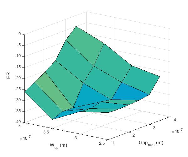
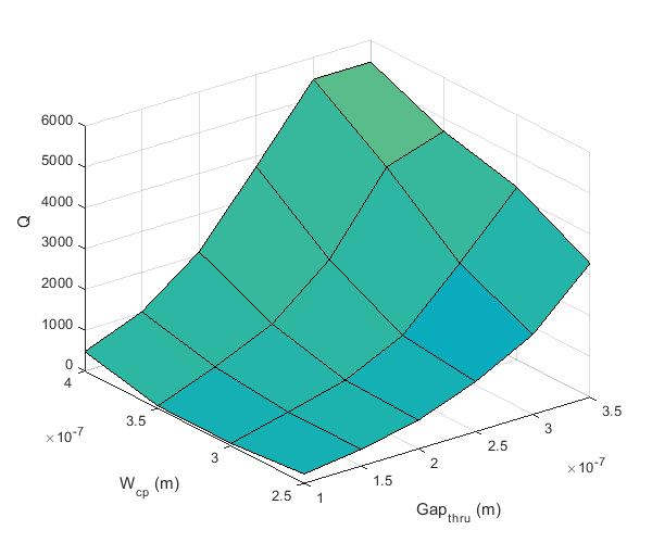
10 Ring Resonator PDK Component W cp G th G dr W cp Vary gaps for a fixed coupler width to achieve critical coupling as determined by quality factor Q and extinction ratio (ER)
11 Lumerical MODE varfdtd Simulation Setup
12 Lumerical Modeling Simulation results
13 Simulation Results cont d.


14 Cadence Virtuoso SKILL Code and Layout

15 Full Reticle


16 Ring Resonator DOE Layout

17 Gt = 150:25:300 Extract Q and ER from Microring Spectra Gd = 175:25:325 Over Coupling Under Coupling

18 Experimental Statistical Data
19 Extract Coupling Coefficients from Q and ER: Equations Define:, L t 2a d c 1 2a c 2 r Q FSR From FSR Under coupling: c R 2 Over coupling: 1 0 c (1 R ) 2 1 (1 0) 2 0 c (1 R ) 2 c (1 R0) a 2 2 a From the transmission at resonance wavelength R 0

20 Extract Coupling Coefficients from Q and ER: Experiments Kappa thru decreases with Gthru Kappa drop decreases with Gdrop There are some unexpected fluctuations, especially in kappa drop
21 Model of Coupling Coefficient vs. Coupling Gap Q Define: 1 2a 2 t L 2 r FSR ( ) Thru port ER 1 2a 2 d Q and ER depend on delta_1 and 2a: 1 2a 1 2a 2 t d Drop port efficiency 2 1 2a 2 Use average of the kappa thru (or drop) a1 = b1 = c1 = 0 a exp( b G ) c t 1 a exp( b G ) c 2a 2 2 d 2 a2 = b2 = c2 = Therefore, we just need to store a1, b1, c1, a2, b2, c2, we could calculate delta_1 and 2a and then the Q and ER
22 Virtuoso Simulated Ring Spectra Gthru = 200 nm x-axis: wavelength in um y-axis: optical power in mw Input optical power = 1mW Gdrop = 175 nm Under-coupling Gdrop = 225 nm Critical-coupling Gdrop = 275 nm Over-coupling
 2016")
23 Virtuoso Schematic Simulations R. Wu, et al., IPR (Vancouver) 2016

24 Virtuoso Simulation Results R. Wu, et al., IPR (Vancouver) 2016
25 Objective: 0.25Tb/s/fiber+ with <5pJ/bit (all inclusive) Low (<10k) Wider channel spacing Less channels Short photon lifetime Higher data rate Low (<10 Gb/s) Easier/Cheaper driver design Lower PD sensitivity and TIA power Cavity Q Data Rate High (>10k) Narrow channel spacing More channels Long photon lifetime Lower data rate High (>10 Gb/s) More challenging driver design Higher PD sensitivity and TIA power What is the crosstalk between two channels given a certain Q, spacing, and data rate? Leakage due to Lorentzian lineshape Sidebands from modulation Spectral Blue shift of Lorentzian


26 Back to Back On-Chip Transceiver 23 lines at 50GHz spacing 5 channel Transmitter Optical Power supply 5 channel Receiver Electrical I/O & power * C. Li et. al. ISSCC 13, IEEE Design & Test 14 * K. Yu et. al. OFC 15, ISSCC 15 * C. H. Chen et. al. OIC 13, 14, 15


27 Back-to-Back Simulation in Virtuoso: Schematic Mod Output Optical Eye PD Photocurrent Electrical Eye 20 Gb/s Gthru = 200 nm Gdrop = 225 nm Critical-coupling


28 Eye Diagrams Laser power increased ~2dB here to improve eye quality Ring Mod: 10 Gb/s 15 Gb/s 20 Gb/s 25 Gb/s On-Chip PD:
29 Device Optical Transmission
30 Experimental Setup Tunable Laser 1 Tunable Laser 2 3dB Combiner 8dB/Grating IL Photonics Chip Tunable Optical Filter + df + df D /D Anritsu PPG D /D Anritsu PPG High-Speed Photodetector (Discovery Semi.) Anritsu BER Anritsu BER DCA Scope

31 Related Experimental Results Seyedi, et al., Photonics in Switching 2016
32 Future Steps Work to improve uniformity and number of comb laser lines DWDM with packaged CMOS driver
33 Thank You
PIC training: Interconnect System Design
 PIC training: Interconnect System Design Keren Bergman PhoenixSim Optical hardware Meisam Bahadori, Sébastien Rumley Lightwave Research Laboratory Columbia University Network Application Silicon Photonics
Large scale optical circuit switches for future data center applications
 Large scale optical circuit switches for future data center applications ONDM2017 workshop Yojiro Moriand Ken-ichi Sato Outline 1. Introduction -Optical circuit switch for datacenter- 2. Sub-switch configuration
Hybrid On-chip Data Networks. Gilbert Hendry Keren Bergman. Lightwave Research Lab. Columbia University
 Hybrid On-chip Data Networks Gilbert Hendry Keren Bergman Lightwave Research Lab Columbia University Chip-Scale Interconnection Networks Chip multi-processors create need for high performance interconnects
Scalable Computing Systems with Optically Enabled Data Movement
 Scalable Computing Systems with Optically Enabled Data Movement Keren Bergman Lightwave Research Laboratory, Columbia University Rev PA1 2 Computation to Communications Bound Computing platforms with increased
High Versatility High Throughput Functional Testing. Robert Polster, David Calhoun, Keren Bergman
 High Versatility High Throughput Functional Testing Robert Polster, David Calhoun, Keren Bergman Challenges of High-Throughput Functional Testing for Scalable Manufacturing Numerous Functional Applications
Optical Interconnects: Trend and Applications
 Optical Interconnects: Trend and Applications Yi-Jen Chan EOL, ITRI Wireless & Optical Communications conference 2008 April 23, 2008 OUTLINE Background and Motivation Trends of Optical Interconnects Technology
AIM Photonics Silicon Photonics PDK Overview. March 22, 2017 Brett Attaway
 AIM Photonics Silicon Photonics PDK Overview March 22, 2017 Brett Attaway Silicon Photonics Process Design Kits (PDK) PDK 3 technologies, 2 major releases/year Full (active)- v1.0 available now Passive-
MARKET PERSPECTIVE: SEMICONDUCTOR TREND OF 2.5D/3D IC WITH OPTICAL INTERFACES PHILIPPE ABSIL, IMEC
 MARKET PERSPECTIVE: SEMICONDUCTOR TREND OF 2.5D/3D IC WITH OPTICAL INTERFACES PHILIPPE ABSIL, IMEC OUTLINE Market Trends & Technology Needs Silicon Photonics Technology Remaining Key Challenges Conclusion
Kotura Analysis: WDM PICs improve cost over LR4
 Kotura Analysis: WDM PICs improve cost over LR4 IEEE P802.3bm - 40 Gb/s & 100 Gb/s Fiber Optic Task Force Sept 2012 Contributors: Mehdi Asghari, Kotura Samir Desai, Kotura Arlon Martin, Kotura Recall the
PIC design across platforms. Ronald Broeke Bright Photonics
 PIC design across platforms Ronald Broeke Bright Photonics OUTLINE Introduction PIC applications & designs MPW Materials & platforms Design modules PICs in Phoxtrot Design House for Photonics ICs Custom
D5.2: Packaging and fiber-pigtailing of the 2 nd generation 2x2 optical interconnect router
 ICT - Information and Communication Technologies Merging Plasmonics and Silicon Photonics Technology towards Tb/s routing in optical interconnects Collaborative Project Grant Agreement Number 249135 D5.2:
How to Simulate and Optimize Integrated Optical Components. Lumerical Solutions, Inc.
 How to Simulate and Optimize Integrated Optical Components Lumerical Solutions, Inc. Outline Introduction Integrated optics for on-chip communication Impact on simulation Simulating planar devices Simulation
IITD OPTICAL STACK : LAYERED ARCHITECTURE FOR PHOTONIC INTERCONNECTS
 SRISHTI PHOTONICS RESEARCH GROUP INDIAN INSTITUTE OF TECHNOLOGY, DELHI 1 IITD OPTICAL STACK : LAYERED ARCHITECTURE FOR PHOTONIC INTERCONNECTS Authors: Janib ul Bashir and Smruti R. Sarangi Indian Institute
Switch Datapath in the Stanford Phictious Optical Router (SPOR)
") Switch Datapath in the Stanford Phictious Optical Router (SPOR) H. Volkan Demir, Micah Yairi, Vijit Sabnis Arpan Shah, Azita Emami, Hossein Kakavand, Kyoungsik Yu, Paulina Kuo, Uma Srinivasan Optics and
Switch Datapath in the Stanford Phictious Optical Router (SPOR) H. Volkan Demir, Micah Yairi, Vijit Sabnis Arpan Shah, Azita Emami, Hossein Kakavand, Kyoungsik Yu, Paulina Kuo, Uma Srinivasan Optics and
1x40 Gbit/s and 4x25 Gbit/s Transmission at 850 nm on Multimode Fiber
 1x40 Gbit/s and 4x25 Gbit/s Transmission at 850 nm on Multimode Fiber, Berlin, Germany J.-R. Kropp, N. Ledentsov, J. Lott, H. Quast Outline 1. Feasibility of components for 4x25G and 1x40G solutions for
Achieve more with light.
 Achieve more with light. Comprehensive suite of leading photonic design tools. Component Design Multiphysics Component Design Lumerical s highly integrated suite of component design tools is purposebuilt
Putting Curves in an Orthogonal World
 Putting Curves in an Orthogonal World Extending the EDA Flow to Support Integrated Photonics Masahiro Shiina October 2018 Traditional IC Design Designers & tool developers have lived in a orthogonal world
AIM Photonics: Manufacturing Challenges for Photonic Integrated Circuits
 AIM Photonics: Manufacturing Challenges for Photonic Integrated Circuits November 16, 2017 Michael Liehr Industry Driving Force EXA FLOP SCALE SYSTEM Blades SiPh Interconnect Network Memory Stack HP HyperX
170 Index. Delta networks, DENS methodology
 Index A ACK messages, 99 adaptive timeout algorithm, 109 format and semantics, 107 pending packets, 105 piggybacking, 107 schematic represenation, 105 source adapter, 108 ACK overhead, 107 109, 112 Active
Developing flexible WDM networks using wavelength tuneable components
 Developing flexible WDM networks using wavelength tuneable components A. Dantcha 1, L.P. Barry 1, J. Murphy 1, T. Mullane 2 and D. McDonald 2 (1) Research Institute for Network and Communications Engineering,
Packaging and Integration Technologies for Silicon Photonics. Dr. Peter O Brien, Tyndall National Institute, Ireland.
 Packaging and Integration Technologies for Silicon Photonics Dr. Peter O Brien, Tyndall National Institute, Ireland. Opportunities for Silicon Photonics Stress Sensors Active Optical Cable 300 mm Silicon
Optical Interconnection Networks in Data Centers: Recent Trends and Future Challenges
 Optical Interconnection Networks in Data Centers: Recent Trends and Future Challenges Speaker: Lin Wang Research Advisor: Biswanath Mukherjee Kachris C, Kanonakis K, Tomkos I. Optical interconnection networks
Optical switching for scalable and programmable data center networks
 Optical switching for scalable and programmable data center networks Paraskevas Bakopoulos National Technical University of Athens Photonics Communications Research Laboratory @ pbakop@mail.ntua.gr Please
Scaling the Compute and High Speed Networking Needs of the Data Center with Silicon Photonics ECOC 2017
 Scaling the Compute and High Speed Networking Needs of the Data Center with Silicon Photonics ECOC 2017 September 19, 2017 Robert Blum Director, Strategic Marketing and Business Development 1 Data Center
Organics in Photonics: Opportunities & Challenges. Louay Eldada DuPont Photonics Technologies
 Organics in Photonics: Opportunities & Challenges Louay Eldada DuPont Photonics Technologies Market Drivers for Organic Photonics Telecom Application Product Examples Requirements What Organics Offer Dynamic
SILICON PHOTONICS WAVEGUIDE AND ITS FIBER INTERCONNECT TECHNOLOGY. Jeong Hwan Song
 SILICON PHOTONICS WAVEGUIDE AND ITS FIBER INTERCONNECT TECHNOLOGY Jeong Hwan Song CONTENTS Introduction of light waveguides Principals Types / materials Si photonics Interface design between optical fiber
Monolithic Integration of Energy-efficient CMOS Silicon Photonic Interconnects
 Monolithic Integration of Energy-efficient CMOS Silicon Photonic Interconnects Vladimir Stojanović Integrated Systems Group Massachusetts Institute of Technology Manycore SOC roadmap fuels bandwidth demand
Hybrid Optoelectronic Router
 Hybrid Optoelectronic Router Ryohei Urata, Tatsushi Nakahara, Hirokazu Takenouchi, Toru Segawa, Ryo Takahashi NTT Photonics Laboratories, NTT Corporation Supported in part by the National Institute of
D5.1: Packaging and fiber-pigtailing of the 2x2 optical interconnect router
 ICT - Information and Communication Technologies Merging Plasmonics and Silicon Photonics Technology towards Tb/s routing in optical interconnects Collaborative Project Grant Agreement Number 249135 D5.1:
Low-Power Reconfigurable Network Architecture for On-Chip Photonic Interconnects
 Low-Power Reconfigurable Network Architecture for On-Chip Photonic Interconnects I. Artundo, W. Heirman, C. Debaes, M. Loperena, J. Van Campenhout, H. Thienpont New York, August 27th 2009 Iñigo Artundo,
Meet in the Middle: Leveraging Optical Interconnection Opportunities in Chip Multi Processors
 Meet in the Middle: Leveraging Optical Interconnection Opportunities in Chip Multi Processors Sandro Bartolini* Department of Information Engineering, University of Siena, Italy bartolini@dii.unisi.it
Silicon Based Packaging for 400/800/1600 Gb/s Optical Interconnects
 Silicon Based Packaging for 400/800/1600 Gb/s Optical Interconnects The Low Cost Solution for Parallel Optical Interconnects Into the Terabit per Second Age Executive Summary White Paper PhotonX Networks
Silicon Photonics for Exascale Systems
 Silicon Photonics for Exascale Systems OFC 2014 Tutorial Keren Bergman Sébastien Rumley, Noam Ophir, Dessislava Nikolova Robert Hendry, Qi Li, Kishore Padmara, Ke Wen, Lee Zhu Lightwave Research Laboratory,
Chapter 7. Widely Tunable Monolithic Laser Diodes
 Chapter 7 Widely Tunable Monolithic Laser Diodes We have seen in Chapters 4 and 5 that the continuous tuning range λ is limited by λ/λ n/n g, where n is the index change and n g the group index of the
Next Generation Requirements for DWDM network
 Next Generation Requirements for DWDM network Roman Egorov Verizon Laboratories May 3, 2011 Verizon copyright 2011. NG Requirements for DWDM network: Outline Optical Transport Network Metro vs. Long-Haul
Moving Forward with the IPI Photonics Roadmap
 Moving Forward with the IPI Photonics Roadmap TWG Chairs: Rich Grzybowski, Corning (acting) Rick Clayton, Clayton Associates Integration, Packaging & Interconnection: How does the chip get to the outside
From Majorca with love
 From Majorca with love IEEE Photonics Society - Winter Topicals 2010 Photonics for Routing and Interconnects January 11, 2010 Organizers: H. Dorren (Technical University of Eindhoven) L. Kimerling (MIT)
 Journal of Advances in Computer Research Quarterly pissn: 2345-606x eissn: 2345-6078 Sari Branch, Islamic Azad University, Sari, I.R.Iran (Vol. 7, No. 3, August 2016), Pages: 47-53 www.jacr.iausari.ac.ir
An Overview of Standard Cell Based Digital VLSI Design
 An Overview of Standard Cell Based Digital VLSI Design With examples taken from the implementation of the 36-core AsAP1 chip and the 1000-core KiloCore chip Zhiyi Yu, Tinoosh Mohsenin, Aaron Stillmaker,
2000 Technology Roadmap Optoelectronics. John Stafford, Motorola January 17, 2001
 2000 Technology Roadmap Optoelectronics John Stafford, Motorola January 17, 2001 Optoelectronic Roadmap Agenda Optoelectronics Market Overview Optical Communications Roadmap Optical Communications Technology
NANOPHOTONIC INTERCONNECT ARCHITECTURES FOR MANY-CORE MICROPROCESSORS
 NANOPHOTONIC INTERCONNECT ARCHITECTURES FOR MANY-CORE MICROPROCESSORS A Dissertation Presented to the Faculty of the Graduate School of Cornell University in Partial Fulfillment of the Requirements for
GEVISTA. CWDM Pluggable OC-48 SFP Transceiver. Description
 CWDM Pluggable OC-48 SFP Transceiver Description The CWDM-OC48-xx-80 is specifically designed for the high performance integrated duplex data transmission over single mode optical fiber. This transceiver
40Gbit/s Coherent Optical Receiver Using a Costas Loop
 1 40Gbit/s Coherent Optical Receiver Using a Costas Loop H. Park, M. Lu, E. Bloch, T. Reed, Z. Griffith, L. Johansson, L. Coldren, and M. Rodwell University of California at Santa Barbara 2 Introductions
1-Fiber Detachable DVI module, DVFX-100
 1-Fiber Detachable DVI module, DVFX-100 DATA SHEET Contents Description Features Applications Technical Specifications Functions Drawing Fiber Connection DVI Pin Description Revision History OPTICIS HQ
Key Challenges in High-End Server Interconnects. Hubert Harrer
 Key Challenges in High-End Server Interconnects by Packaging Key Challenges Bus Bandwidths Large increase of bandwidths driven by multicore processors increasing frequency increasing bit lines Power high
Brief Background in Fiber Optics
 The Future of Photonics in Upcoming Processors ECE 4750 Fall 08 Brief Background in Fiber Optics Light can travel down an optical fiber if it is completely confined Determined by Snells Law Various modes
RSoft Product Applications
 RSoft Product Applications Complete design solutions for photonic components, circuits and systems synopsys.com/optical-solutions/rsoft RSoft Photonic Design Software Applications Synopsys RSoft products
Trickle Up: Photonics and the Future of Computing Justin Rattner Chief Technology Officer Intel Corporation
 Trickle Up: Photonics and the Future of Computing Justin Rattner Chief Technology Officer Intel Corporation * Other names, logos and brands may be claimed as the property of others. Copyright 2009, Intel
NETWORKS-ON-CHIP (NoC) plays an important role in
 plays an important role in") 3736 JOURNAL OF LIGHTWAVE TECHNOLOGY, VOL. 30, NO. 23, DECEMBER 1, 2012 A Universal Method for Constructing N-Port Nonblocking Optical Router for Photonic Networks-On-Chip Rui Min, Ruiqiang Ji, Qiaoshan
3736 JOURNAL OF LIGHTWAVE TECHNOLOGY, VOL. 30, NO. 23, DECEMBER 1, 2012 A Universal Method for Constructing N-Port Nonblocking Optical Router for Photonic Networks-On-Chip Rui Min, Ruiqiang Ji, Qiaoshan
Future of Interconnect Fabric A Contrarian View. Shekhar Borkar June 13, 2010 Intel Corp. 1
 Future of Interconnect Fabric A ontrarian View Shekhar Borkar June 13, 2010 Intel orp. 1 Outline Evolution of interconnect fabric On die network challenges Some simple contrarian proposals Evaluation and
2Mbps 850nm MMF SFP Transceiver 2km HOLS-P1850-LD-CV-B
 Features: Compliant with SFP MSA standard 3.3V DC power supply 850nm VCSEL, 2Mbps, 2km Built-in dtionsigital diagnostic function Difference LVPECL inputs and outputs Duplex LC connector Compliant with
A Single Grating-lens Focusing Two Orthogonally Polarized Beams in Opposite Direction
 , pp.41-45 http://dx.doi.org/10.14257/astl.2016.140.08 A Single Grating-lens Focusing Two Orthogonally Polarized Beams in Opposite Direction Seung Dae Lee 1 1* Dept. of Electronic Engineering, Namseoul
Intel Silicon Photonics: from Research to Product
 IEEE Components, Packaging and Manufacturing Technology Chapter, Santa Clara Valley 3/8/2017 Intel Silicon Photonics: from Research to Product MARCH 8, 2017 Ling Liao Principal Engineer Silicon Photonics
UBCx Phot1x: Silicon Photonics Design, Fabrication and Data Analysis
 UBCx Phot1x: Silicon Photonics Design, Fabrication and Data Analysis Course Syllabus Table of Contents Course Syllabus 1 Course Overview 1 Course Learning Objective 1 Course Philosophy 1 Course Details
Packaging avancé pour les modules photoniques
 I N S T I T U T D E R E C H E R C H E T E C H N O L O G I Q U E Packaging avancé pour les modules photoniques S. Bernabé, CEA-Leti Marc Epitaux, SAMTEC Workshop «Photonique sur Silicium, une rupture attendue»
DC Network Connectivity
 DC Network Connectivity Options & Optimizing TCO Rakesh SAMBARAJU - Application Engineer Nexans Data Center Solutions Agenda l Part I Ethernet Standards and Technologies Ø Current Ethernet Standards Ø
All Optical Packet Switches Based On Space Switch Array for the Transmission of Higher Data Rate Using NRZand RZ Modulation
 IOSR Journal of Electronics and Communication Engineering (IOSR-JECE) e-issn: 2278-2834,p- ISSN: 2278-8735.Volume 9, Issue 2, Ver. VII (Mar - Apr. 2014), PP 19-24 All Optical Packet Switches Based On Space
100 Gb/s SMF Standard Broad Market Potential Observations
 100 Gb/s SMF Standard Broad Market Potential Observations Next Generation 100Gb/s Ethernet Optics Study Group IEEE 802.3 Interim Session Newport Beach, CA 24-25 January 2012 Chris Cole chris.cole@finisar.com
Exascale challenges. June 27, Ecole Polytechnique Palaiseau France
 Exascale challenges June 27,28 2012 Ecole Polytechnique Palaiseau France patrick.demichel@hp.com HP Labs around the world Beijing Tokyo Palo Alto Bristol St. Petersburg Bangalore 7 locations 600 researchers
Photonics Integration in Si P Platform May 27 th Fiber to the Chip
 Photonics Integration in Si P Platform May 27 th 2014 Fiber to the Chip Overview Introduction & Goal of Silicon Photonics Silicon Photonics Technology Wafer Level Optical Test Integration with Electronics
Cisco MDS 9000 Family Pluggable Transceivers
 Cisco MDS 9000 Family Pluggable Transceivers The Cisco Small Form-Factor Pluggable (), and X2 devices for use on the Cisco MDS 9000 Family are hot-swappable transceivers that plug into ports on the Cisco
High Speed Optical Link Based on Integrated Silicon Photonics
 High Speed Optical Link Based on Integrated Silicon Photonics Dr. Haisheng Rong Photonics Research Lab Intel Corporation www.intel.com/go/sp PKU, Summer School July 04, 2012 Agenda Motivation Electronic
VCSEL Technology and Digital
 VCSEL Technology and Digital Applications Marco Ghisoni Zarlink Semiconductor AB marco.ghisoni@zarlink.com Outline Introduction Today's Digital Applications Mass market Parallel optical modules Future
Silicon Photonics: Failing to Deliver on WDM Promises for the Datacenter
 Silicon Photonics: Failing to Deliver on WDM Promises for the Datacenter Silicon Photonics: Is it still in hype or on its way to the field? OFC 2015 Workshop 22 March 2015 Chris Cole Mainstream Datacenter
Jeff Kash, Dan Kuchta, Fuad Doany, Clint Schow, Frank Libsch, Russell Budd, Yoichi Taira, Shigeru Nakagawa, Bert Offrein, Marc Taubenblatt
 IBM Research PCB Overview Jeff Kash, Dan Kuchta, Fuad Doany, Clint Schow, Frank Libsch, Russell Budd, Yoichi Taira, Shigeru Nakagawa, Bert Offrein, Marc Taubenblatt November, 2009 November, 2009 2009 IBM
AD-A STARNET: 1) A MultiGbit/s Optical Local Area Network With Both Packet and Circuit Switching IX MAR I94l. IVo 0 o 0q -5i-:U-- I SS7
 A MultiGbit/s Optical Local Area Network With Both Packet and Circuit Switching IX MAR I94l. IVo 0 o 0q -5i-:U-- I SS7") l-c I "^ J,' 1 AD-A247 617 DTIC IX MAR 18192 STARNET: 1) A MultiGbit/s Optical Local Area Network With Both Packet and Circuit Switching I94l L. Kazovsky, P. Poggiolini Department of Electrical Engineering,
l-c I "^ J,' 1 AD-A247 617 DTIC IX MAR 18192 STARNET: 1) A MultiGbit/s Optical Local Area Network With Both Packet and Circuit Switching I94l L. Kazovsky, P. Poggiolini Department of Electrical Engineering,
Intra Optical Data Center Interconnection Session 2: Debating Intra-DC solutions and Photonic Integration approaches
 Intra Optical Data Center Interconnection Session 2: Debating Intra-DC solutions and Photonic Integration approaches Co-Organizer/Presider/Session Chair: Dr. Ioannis Tomkos Networks and Optical Communications
EXASCALE COMPUTING: WHERE OPTICS MEETS ELECTRONICS
 EXASCALE COMPUTING: WHERE OPTICS MEETS ELECTRONICS Overview of OFC Workshop: Organizers: Norm Jouppi HP Labs, Moray McLaren HP Labs, Madeleine Glick Intel Labs March 7, 2011 1 AGENDA Introduction. Moray
Low latency and efficient optical flow control for intra data center networks
 Low latency and efficient optical flow control for intra data center networks Wang Miao, * Stefano Di Lucente, Jun Luo, Harm Dorren, and Nicola Calabretta COBRA Research Institute, Eindhoven University
Active Optical Cables. Dr. Stan Swirhun VP & GM, Optical Communications April 2008
 Active Optical Cables Dr. Stan Swirhun VP & GM, Optical Communications April 2008 Supplier of Mixed Signal Products Supplier of Mixed Signal Communication Semiconductors, public $230M Medical Communications
Building petabit/s data center network with submicroseconds latency by using fast optical switches Miao, W.; Yan, F.; Dorren, H.J.S.; Calabretta, N.
 Building petabit/s data center network with submicroseconds latency by using fast optical switches Miao, W.; Yan, F.; Dorren, H.J.S.; Calabretta, N. Published in: Proceedings of 20th Annual Symposium of
PSMC Roadmap For Integrated Photonics Manufacturing
 PSMC Roadmap For Integrated Photonics Manufacturing Richard Otte Promex Industries Inc. Santa Clara California For the Photonics Systems Manufacturing Consortium April 21, 2016 Meeting the Grand Challenges
OPTICAL INTERCONNECTS IN DATA CENTER. Tanjila Ahmed
 OPTICAL INTERCONNECTS IN DATA CENTER Tanjila Ahmed Challenges for Today s Data Centers Challenges to be Addressed : Scalability Low latency Energy Efficiency Lower Cost Challenges for Today s Data Center
A New Model for Optical Crosstalk in SinglePhoton Avalanche Diodes Arrays
 A New Model for Optical Crosstalk in SinglePhoton Avalanche Diodes Arrays I. Rech, A. Ingargiola, R. Spinelli, S. Marangoni, I. Labanca, M. Ghioni, S. Cova Dipartimento di Elettronica ed Informazione Politecnico
Silicon Photonics Scalable Design Framework:
 Silicon Photonics Scalable Design Framework: From Design Concept to Physical Verification Hossam Sarhan Technical Marketing Engineer hossam_sarhan@mentor.com Objective: Scalable Photonics Design Infrastructure
Analyzing the Effectiveness of On-chip Photonic Interconnects with a Hybrid Photo-electrical Topology
 Analyzing the Effectiveness of On-chip Photonic Interconnects with a Hybrid Photo-electrical Topology Yong-jin Kwon Department of EECS, University of California, Berkeley, CA Abstract To improve performance
OPAL: A Multi-Layer Hybrid Photonic NoC for 3D ICs
 OPAL: A Multi-Layer Hybrid Photonic NoC for 3D ICs 4B-1 Sudeep Pasricha, Shirish Bahirat Colorado State University, Fort Collins, CO {sudeep, shirish.bahirat}@colostate.edu Abstract - Three-dimensional
Virtuoso - Enabled EPDA framework AIM SUNY Process
 Virtuoso - Enabled EPDA framework AIM SUNY Process CADENCE, LUMERICAL, PHOENIX SOFTWARE Driven by our customers Cadence is the leader with Virtuoso custom design platform for electronics custom and mixed
Next Generation Transceivers: The Roadmap Component Driver Contributions from Roadmap team. Dominic O Brien Mike Schabel
 Next Generation Transceivers: The Roadmap Component Driver Contributions from Roadmap team Dominic O Brien Mike Schabel Outline New markets Key challenges Potential evolution Recommendations Fibre to the
Electro-optic Switches Based on Space Switching of Multiplexed WDM Signals: Blocking vs Non-blocking Design Trade-offs
 1 Electro-optic Switches Based on Space Switching of Multiplexed WDM Signals: Blocking vs Non-blocking Design Trade-offs Apostolos Siokis a,c, Konstantinos Christodoulopoulos b,c, Nikos Pleros d, Emmanouel
The MIT Communications Technology Roadmap Program IPI TWG Report
 The MIT Communications Technology Roadmap Program IPI TWG Report May 19, 2006 Louay Eldada Integration, Packaging & Interconnection Technology Working Group CTO, VP Engineering DuPont Photonics Chair,
A block diagram of the HXFP-XDX1XX XFP optical transceiver is shown below
 Features Support 9.95 Gb/s to 11.3 Gb/s serial optical and electrical interface Temperature Stabilized DWDM EML Transmitter 1550nm cooled EML transmitter with TEC and PIN receiver Both 40Km and 80Km Units
Network-on-Chip Architecture
 Multiple Processor Systems(CMPE-655) Network-on-Chip Architecture Performance aspect and Firefly network architecture By Siva Shankar Chandrasekaran and SreeGowri Shankar Agenda (Enhancing performance)
A mm 2 780mW Fully Synthesizable PLL with a Current Output DAC and an Interpolative Phase-Coupled Oscillator using Edge Injection Technique
 A 0.0066mm 2 780mW Fully Synthesizable PLL with a Current Output DAC and an Interpolative Phase-Coupled Oscillator using Edge Injection Technique Wei Deng, Dongsheng Yang, Tomohiro Ueno, Teerachot Siriburanon,
1250Mbps 850nm MF SFP Transceiver 550m HOLS-PG85Z-LN-CV/PG85Z-LD-CV
 Features: Compliant with SFP MSA standard Compliant with IEEE 802.3z 3.3V DC power supply 850nm, VCSEL, 1250Mbps, 550m; Compliance with 10 Base-FL, 100Base-SX and 1000Base-SX Difference LVPECL inputs and
Optical Evaluation Kit for the ADN2530 Differential VCSEL Driver EVAL-ADN2530
 Optical Evaluation Kit for the ADN2530 Differential VCSEL Driver EVAL-ADN2530 GENERAL DESCRIPTION This data sheet describes the optical evaluation kit for the ADN2530, a 10 Gbps active back-terminated,
HPC Technology Trends
 HPC Technology Trends High Performance Embedded Computing Conference September 18, 2007 David S Scott, Ph.D. Petascale Product Line Architect Digital Enterprise Group Risk Factors Today s s presentations
SOI at the heart of the silicon photonics design. Arnaud Rigny, Business Development Manager Semicon Europa, TechArena
 SOI at the heart of the silicon photonics design Arnaud Rigny, Business Development Manager Semicon Europa, TechArena Outline 1 Market demand for optical interconnect 2 Silicon on Insulator for optical
Ethernet OptoLock EDL300T
 Ethernet OptoLock EDL300T DATA SHEET 650 nm 100 Mbps Ethernet Fiber Optic Transceiver with Termination for Bare POF Seamless Digital to Light/ Light to Digital Conversion FEATURES Simple low-cost termination
A 3-stage CLOS architecture for high-throughput optical packet switching
 Invited Paper A 3-stage CLOS architecture for high-throughput optical packet switching H.J.S. Dorren, Nicola Calabretta and Oded Raz COBRA Research Institute, Eindhoven University of Technology, P.O. Box
Hybrid Integration of a Semiconductor Optical Amplifier for High Throughput Optical Packet Switched Interconnection Networks
 Hybrid Integration of a Semiconductor Optical Amplifier for High Throughput Optical Packet Switched Interconnection Networks Odile Liboiron-Ladouceur* and Keren Bergman Columbia University, 500 West 120
Graphene-enabled hybrid architectures for multiprocessors: bridging nanophotonics and nanoscale wireless communication
 Graphene-enabled hybrid architectures for multiprocessors: bridging nanophotonics and nanoscale wireless communication Sergi Abadal*, Albert Cabellos-Aparicio*, José A. Lázaro, Eduard Alarcón*, Josep Solé-Pareta*
New Data Center and Transport Interconnect Technology
 New Data Center and Transport Interconnect Technology Tom McDermott Fujitsu Network Communications, Inc. October 30, 2014 Changing Requirements Datacenters are expanding in size. Continued need for 100m
Johnnie Chan and Keren Bergman VOL. 4, NO. 3/MARCH 2012/J. OPT. COMMUN. NETW. 189
 Johnnie Chan and Keren Bergman VOL. 4, NO. 3/MARCH 212/J. OPT. COMMUN. NETW. 189 Photonic Interconnection Network Architectures Using Wavelength-Selective Spatial Routing for Chip-Scale Communications
Reliability-Performance Trade-offs in Photonic NoC Architectures
 Rochester Institute of Technology RIT Scholar Works Theses Thesis/Dissertation Collections 9-2013 Reliability-Performance Trade-offs in Photonic NoC Architectures Pradheep Khanna Kaliraj Follow this and
Hands-On Fiber Optic Designer
 Hands-On Course Description Fiber optic systems are a key part of new communications services. Teir success depends upon good design. This Hands-On course will cover the particulars of how fiber optic
PLANAR LIGHTWAVE CIRCUITS FOR USE IN ADVANCED OPTICAL INSTRUMENTATION
 PLANAR LIGHTWAVE CIRCUITS FOR USE IN ADVANCED OPTICAL INSTRUMENTATION AN ENABLENCE ARTICLE WRITTEN BY DR. MATT PEARSON, VP TECHNOLOGY & ASHOK BALAKRISHNAN, DIRECTOR OF PRODUCT DEVELOPMENT PUBLISHED IN
Integrated Optical Devices
 Integrated Optical Devices May 2018 Integrated Optical Devices 2017 a good year for Silicon Photonics, a fantastic year for integrated InP and GaAs optics Source: Luxtera with text added by LightCounting
Development of Optical Wiring Technology for Optical Interconnects
 Development of Optical Wiring Technology for Optical Interconnects Mitsuhiro Iwaya*, Katsuki Suematsu*, Harumi Inaba*, Ryuichi Sugizaki*, Kazuyuki Fuse*, Takuya Nishimoto* 2, Kenji Kamoto* 3 We had developed
On Board Optical Interconnection A Joint Development Project Consortium. Terry Smith & John MacWilliams October 31, 2016
 On Board Optical Interconnection A Joint Development Project Consortium Terry Smith & John MacWilliams October 31, 2016 Presentation Outline Executive Summary Issues in Board-Level Optical Interconnect