inemi Roadmap Packaging and Component Substrates TWG
|
|
|
- Polly Price
- 6 years ago
- Views:
Transcription


1 inemi Roadmap Packaging and Component Substrates TWG TWG Leaders: W. R. Bottoms William Chen Presented by M. Tsuriya

2 Agenda Situation Everywhere in Electronics Evolution & Blooming Drivers Changing inemi Roadmap 21 TWGs, Outline, Cross TWG Activities Rapid Change in Requirement Material Single Chip Package WLP Complexity 2.5D/3D Integration Embedded Packages Future Co-Integrated SiP Conclusion Schedule 2

3 Everywhere in Electronics 3 Source: Yole at inemi Package workshop 2014


4 Evolution & Blooming Flowers 4 Source: Yole at inemi Package workshop 2014

5 Drivers Changing.. This requires change in packages Requirement High Band Density Low Latency Expanded Data Processing Expanded data Storage Major Gaps Power (particularly Package Related) Thermal Management Cost Heterogeneous Integration Physical Density of Bandwidth Latency 5

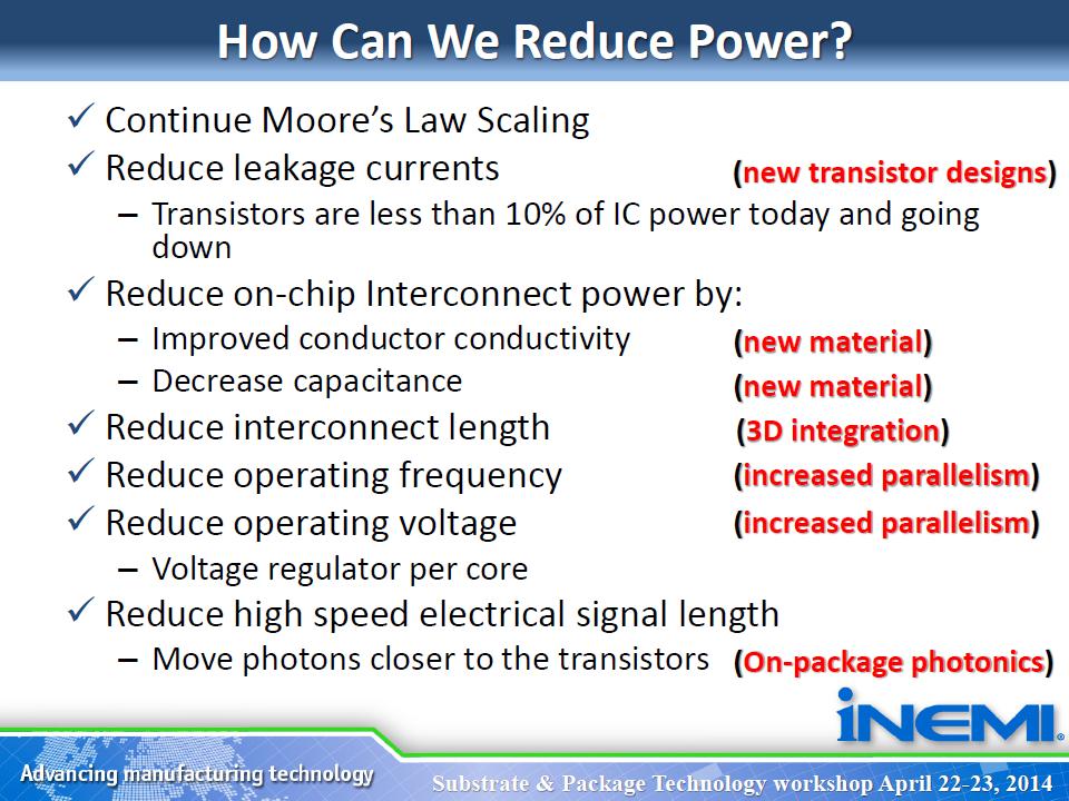
6 6 Power Reduction
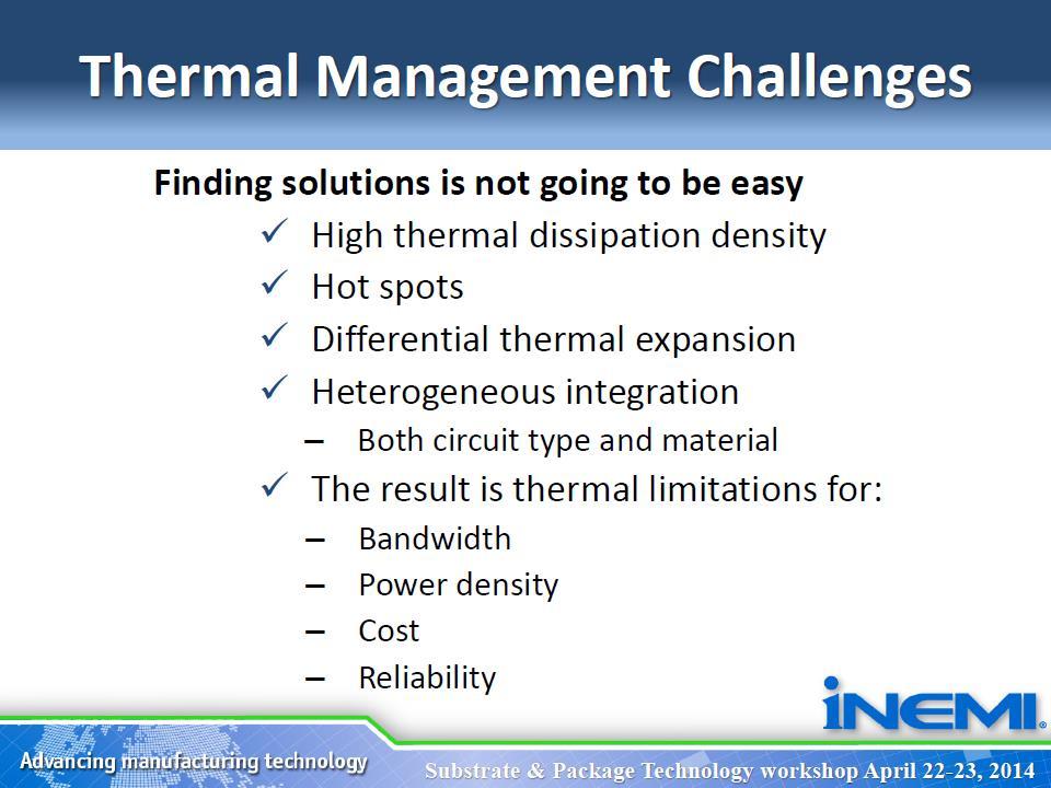
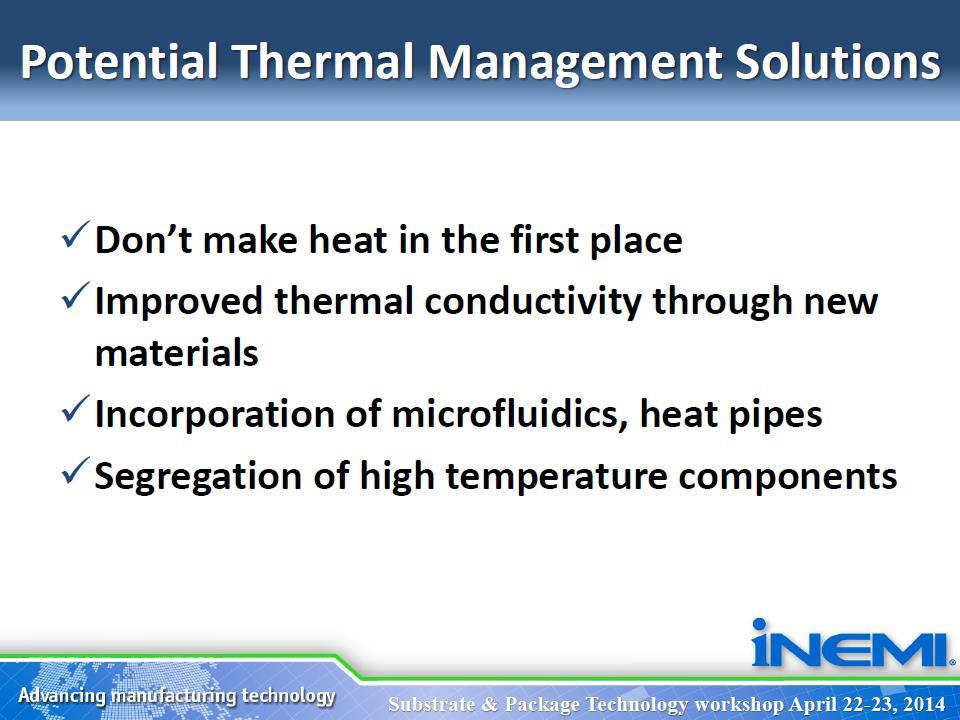

7 7 Thermal Management
8 Chapter Outline Executive Summary Introduction Situation Analysis - bench mark state of the art Packaging and Substrate Markets Roadmap of Quantified Key Attribute Needs Single Chip Packaging Component Substrates Wafer Level Packaging 3D integration MEMS Packaging Automotive Electronics SiP Packaging Gaps and Showstoppers Recommendations for Potential Alternative Technologies Critical Research Needs Contributors 9
9 Cross TWG Activity Technology Working Group / PEG Semiconductor Technology x x Final Assembly x Interconnect PCB (Organic) x x Modeling, Simulation & Design Tools x Optoelectronics x x Packaging & Component Substrates x RF Components & Subsystems x x Test, Inspection and Measurement x x Thermal Management x x Board Assembly x x Passive Components x x Interconnect Substrates (Ceramic) x Electronic Connectors x x MEMS/Sensors x Photovoltaics x Power Conversion Electronics x x Office / Consumer x x Portable / Wireless x x Automotive x x High-End Systems x x Medical x x Aerospace/Defense x x 10

10 11 All Materials will Change
11 Single-Chip Package Technology Year of Production Cost per Pin Minimum for Contract Assembly (Cents/Pin) Low-end, Low-cost package Mobile Device Package Memory Cost-performance High-performance Harsh Performance: chip-to-chip Low-end, Low-cost package(mhz) Mobile Device Package(MHz) Memory(MHz) Cost-performance (Gb/s) High-performance (Gb/s) Harsh Performance: Pkg-to-Board Manufacturable solutions exist, and are being optimized Manufacturable solutions are known Interim solutions are known Manufacturable solutions are NOT known Low-end, Low-cost package(mhz) Mobile Device Package(MHz) Memory(MHz) Cost-performance (Gb/s) High-performance (Gb/s)
12 The Rapid Change in Requirement is Driving a Revolution in Packaging New Material New Package Architecture 2.5D Packages Wafer Level Packages System Integration in a Package (SiP) New Manufacturing Process Cu Pillar No Underfills Panel Level Processing 13

13 New Materials Will Be Required Many are in use today Many are in development Cu interconnect Ultra Low k dielectrics High k dielectrics Organic semiconductors Green Materials Pb free Halogen free Nanotubes Nano Wires Macromolecules Nano Particles Composite materials But improvements are needed 14

14 15 WLP Complexity is Rising

15 16 2.5D/ 3D Integration
16 Future Co-Integrated SiP TSV memory stack, direct bonding interconnect, serdes in controller Electronics, Photonics and Plasmonics on an SOI Substrate Photonic engine Large on-package memory cache with serdes in controller DRAM DRAM DRAM DRAM Memory controller CMOS logic Flash memory Flash memory Flash memory Flash memory DRAM DRAM Memory controller Multiple voltage regulators to match power delivery to each component to the work in process Silicon Substrate with TSV interconnects and Si Waveguides Power Controller Photonic/electronic Circuit Board 17 PCB with electronic and photonic signals with embedded components
17 New Package Architectures Gaps & Challenges Gap 3D TSV Integration Cost Test Strategy Thermal Management Signal and Power Integrity Handing Thin Die/Wafer Bonding System in Package Change Needed Close the gap between Chip and Substrate Wiring Packaging for Higher Current Density Flexible System Packaging 3D Packaging Low Cost Package Manufacturing Processes for Complex wafer Level Packages Photonic to the Package Heterogeneous Integration Noise/Cross Talk Thermal Management Wafer Level Packaging Rapidly Increasing Complexity in WLP Contact Pitch 2013 Edition 2015 Edition Wafer2Wafer Bonding 18
18 Conclusion System Integration at the package level is the only path to meet the cost and Performance Requirement over the next ten years. The definition of research needs for new materials, new architectures and new manufacturing equipment and process is essential to ensure that solutions are ready before Gaps become Showstoppers. inemi roadmap is focused on meeting that needs. 19

19 2015 Roadmap Schedule 3Q2013: Recruit Product Sector Champions, teams and refine data charts/begin 2015 Roadmap Newsletter & send 2013 PEG chapters 3/4Q13: Product Sector Champions Develop Emulators September 16, 2013 Teleconference with P.E. Group Chairs September 27, 2013 Web based meeting TWG/PEG Chairs (key attributes) October 16, 2013 SMTAI Presentation on 2015 Plans October 17, Roadmap PEG Kick-off with PEG/TWG/TC at SMTAI 2013 Roadmap chapter, format, Exec. Summary ed to each TWG chair (Word) 1/3/2014 Organizing Teleconference with TWG Chairs 1/10/2014: Feb 19, PEG Workshop/TWG Kick-off Agilent Technologies, Santa Rosa, CA Product Sector Tables Complete PEG Chapter rough drafts written Cross cut issues are initially addressed May 13, 2014 Telecon With TWG Chairs, Preliminary PEG Chapters Due May 27, 2014 N.A. RM WS - Open Roadmap TWG Presentations in Orlando, FL (ECTC) June 11, 2014 European Roadmap Workshop/Webinar 9:00 AM EDT June 18, 2014 Asian Roadmap Workshop/Webinar 8:00 PM EDT July 14, 2014 TWG Drafts Due for TC Review August 20,21, 2014 TC Face-to-Face Review with TWG Chairs at IBM, RTP, N.C. September 22, 2014 Final Chapters of Roadmap Due October 2, 2014 TC Briefing/SMTA at SMTAI (Rosemont, Illinois) October 31, 2014 Edit, Prepare Appendix A-D, Executive Summary November 20, 2014 Go To Press December TBD, 2014 Ship to Members April TBD, 2015 Offer to Industry April TBD, 2015 Global industry roadmap presentations via webinars 20 20

20 Bill Bader Grace O Malley gomalley@inemi.org
inemi Roadmap and Technical Plan on Organic PCB Bill Bader, inemi inemi PCB/Laminate Workshop, Taipei October 22, 2013
 inemi Roadmap and Technical Plan on Organic PCB Bill Bader, inemi inemi PCB/Laminate Workshop, Taipei October 22, 2013 Agenda inemi Roadmap Process and Scope 2013 PCB Roadmap and TIG Outcomes Summary &
Trends and Challenges for Data Centers inemi Roadmap
 Trends and Challenges for Data Centers inemi Roadmap Trends and Challenges Context what's happening in the market and in the industry Changes new technology developments Challenges what is needed for the
PSMC Roadmap For Integrated Photonics Manufacturing
 PSMC Roadmap For Integrated Photonics Manufacturing Richard Otte Promex Industries Inc. Santa Clara California For the Photonics Systems Manufacturing Consortium April 21, 2016 Meeting the Grand Challenges
Introduction to inemi. Dr. Robert Pfahl VP of Global Operations
 Introduction to Dr. Robert Pfahl VP of Global Operations About Mission: Forecast and Accelerate improvements in the Electronics Manufacturing Industry for a Sustainable Future. 5 Key Deliverables: Technology
Heterogeneous Integration and the Photonics Packaging Roadmap
 Heterogeneous Integration and the Photonics Packaging Roadmap Presented by W. R. Bottoms Packaging Photonics for Speed & Bandwidth The Functions Of A Package Protect the contents from damage Mechanical
3D Integration & Packaging Challenges with through-silicon-vias (TSV)
") NSF Workshop 2/02/2012 3D Integration & Packaging Challenges with through-silicon-vias (TSV) Dr John U. Knickerbocker IBM - T.J. Watson Research, New York, USA Substrate IBM Research Acknowledgements IBM
NSF Workshop 2/02/2012 3D Integration & Packaging Challenges with through-silicon-vias (TSV) Dr John U. Knickerbocker IBM - T.J. Watson Research, New York, USA Substrate IBM Research Acknowledgements IBM
Packaging Challenges. Driven By The IoT And Migration To The Cloud. Presented by: W. R. Bottoms
 Packaging Challenges Driven By The IoT And Migration To The Cloud Presented by: W. R. Bottoms Emerging Technology Drivers There are 2 market driven trends forcing more fundamental change on the industry
inemi Roadmap A Systems Approach to Closing Technology Gaps
 inemi Roadmap A Systems Approach to Closing Technology Gaps Presented at : Microsystems: Embedded Software + Hardware Transforming the Innovation Landscape Jim McElroy, inemi Oct. 10/11, 2012 Topics inemi
ARCHIVE 2008 COPYRIGHT NOTICE
 Keynote Speaker ARCHIVE 2008 Packaging & Assembly in Pursuit of Moore s Law and Beyond Karl Johnson Ph.D. Vice President and Senior Fellow Advanced Packaging Systems Integration Laboratory Freescale Semiconductor
Advanced Packaging For Mobile and Growth Products
 Advanced Packaging For Mobile and Growth Products Steve Anderson, Senior Director Product and Technology Marketing, STATS ChipPAC Growing Needs for Silicon & Package Integration Packaging Trend Implication
Implementing the System-in-Package Technical Plan. Productronica 17 November, 2005
 Implementing the System-in-Package Technical Plan Productronica 17 November, 2005 0 Agenda 09:00 Welcome and Introduction Jim McElroy 09:10 inemi Technical Planning Process Jim McElroy 09:20 inemi SIP
2018 Project Focus of IPSR. Dr. Robert C. Pfahl Director of Roadmapping March 12, 2018 OFC
 2018 Project Focus of IPSR Dr. Robert C. Pfahl Director of Roadmapping March 12, 2018 OFC Sponsors & Participants Sponsor Lead Participants 1 Goals and Objectives of IPSR Goals Create A Self-Sustaining
Intro to: Ultra-low power, ultra-high bandwidth density SiP interconnects
 This work was supported in part by DARPA under contract HR0011-08-9-0001. The views, opinions, and/or findings contained in this article/presentation are those of the author/presenter
From 3D Toolbox to 3D Integration: Examples of Successful 3D Applicative Demonstrators N.Sillon. CEA. All rights reserved
 From 3D Toolbox to 3D Integration: Examples of Successful 3D Applicative Demonstrators N.Sillon Agenda Introduction 2,5D: Silicon Interposer 3DIC: Wide I/O Memory-On-Logic 3D Packaging: X-Ray sensor Conclusion
TechSearch International, Inc.
 Silicon Interposers: Ghost of the Past or a New Opportunity? Linda C. Matthew TechSearch International, Inc. www.techsearchinc.com Outline History of Silicon Carriers Thin film on silicon examples Multichip
Chapter 0 Introduction
 Chapter 0 Introduction Jin-Fu Li Laboratory Department of Electrical Engineering National Central University Jhongli, Taiwan Applications of ICs Consumer Electronics Automotive Electronics Green Power
WLSI Extends Si Processing and Supports Moore s Law. Douglas Yu TSMC R&D,
 WLSI Extends Si Processing and Supports Moore s Law Douglas Yu TSMC R&D, chyu@tsmc.com SiP Summit, Semicon Taiwan, Taipei, Taiwan, Sep. 9 th, 2016 Introduction Moore s Law Challenges Heterogeneous Integration
Monolithic 3D Integration using Standard Fab & Standard Transistors. Zvi Or-Bach CEO MonolithIC 3D Inc.
 Monolithic 3D Integration using Standard Fab & Standard Transistors Zvi Or-Bach CEO MonolithIC 3D Inc. 3D Integration Through Silicon Via ( TSV ), Monolithic Increase integration Reduce interconnect total
Define material specifications for high power and high density PCB's needed to support under-the-hood automotive applications
 Define material specifications for high power and high density PCB's needed to support under-the-hood automotive applications Call for Project Formation December, 2015 Initiative Leaders: Steve Brown,
3D systems-on-chip. A clever partitioning of circuits to improve area, cost, power and performance. The 3D technology landscape
 Edition April 2017 Semiconductor technology & processing 3D systems-on-chip A clever partitioning of circuits to improve area, cost, power and performance. In recent years, the technology of 3D integration
3D SYSTEM INTEGRATION TECHNOLOGY CHOICES AND CHALLENGE ERIC BEYNE, ANTONIO LA MANNA
 3D SYSTEM INTEGRATION TECHNOLOGY CHOICES AND CHALLENGE ERIC BEYNE, ANTONIO LA MANNA OUTLINE 3D Application Drivers and Roadmap 3D Stacked-IC Technology 3D System-on-Chip: Fine grain partitioning Conclusion
TechSearch International, Inc.
 On the Road to 3D ICs: Markets and Solutions E. Jan Vardaman President TechSearch International, Inc. www.techsearchinc.com High future cost of lithography Severe interconnect delay Noted in ITRS roadmap
Wafer Level Packaging The Promise Evolves Dr. Thomas Di Stefano Centipede Systems, Inc. IWLPC 2008
 Wafer Level Packaging The Promise Evolves Dr. Thomas Di Stefano Centipede Systems, Inc. IWLPC 2008 / DEVICE 1.E+03 1.E+02 1.E+01 1.E+00 1.E-01 1.E-02 1.E-03 1.E-04 1.E-05 1.E-06 1.E-07 Productivity Gains
Roadmap Trends and Emerging Technologies. Bob Pfahl
 Roadmap Trends and Emerging Technologies Bob Pfahl 2007 Roadmap Topics 2007 Research Priorities Key Gaps By Roadmap Areas By Research Areas Projects to address inemi Strategic Thrusts Conclusions and Summary
Vertical Circuits. Small Footprint Stacked Die Package and HVM Supply Chain Readiness. November 10, Marc Robinson Vertical Circuits, Inc
 Small Footprint Stacked Die Package and HVM Supply Chain Readiness Marc Robinson Vertical Circuits, Inc November 10, 2011 Vertical Circuits Building Blocks for 3D Interconnects Infrastructure Readiness
Emerging IC Packaging Platforms for ICT Systems - MEPTEC, IMAPS and SEMI Bay Area Luncheon Presentation
 Emerging IC Packaging Platforms for ICT Systems - MEPTEC, IMAPS and SEMI Bay Area Luncheon Presentation Dr. Li Li Distinguished Engineer June 28, 2016 Outline Evolution of Internet The Promise of Internet
Packaging Innovation for our Application Driven World
 Packaging Innovation for our Application Driven World Rich Rice ASE Group March 14 th, 2018 MEPTEC / IMAPS Luncheon Series 1 What We ll Cover Semiconductor Roadmap Drivers Package Development Thrusts Collaboration
Advancing high performance heterogeneous integration through die stacking
 Advancing high performance heterogeneous integration through die stacking Suresh Ramalingam Senior Director, Advanced Packaging European 3D TSV Summit Jan 22 23, 2013 The First Wave of 3D ICs Perfecting
Packaging Technology for Image-Processing LSI
 Packaging Technology for Image-Processing LSI Yoshiyuki Yoneda Kouichi Nakamura The main function of a semiconductor package is to reliably transmit electric signals from minute electrode pads formed on
3D technology for Advanced Medical Devices Applications
 3D technology for Advanced Medical Devices Applications By, Dr Pascal Couderc,Jerome Noiray, Dr Christian Val, Dr Nadia Boulay IMAPS MEDICAL WORKSHOP DECEMBER 4 & 5,2012 P.COUDERC 3D technology for Advanced
High Volume Manufacturing Supply Chain Ecosystem for 2.5D HBM2 ASIC SiPs
 Open-Silicon.com 490 N. McCarthy Blvd, #220 Milpitas, CA 95035 408-240-5700 HQ High Volume Manufacturing Supply Chain Ecosystem for 2.5D HBM2 ASIC SiPs Open-Silicon Asim Salim VP Mfg. Operations 20+ experience
Bringing 3D Integration to Packaging Mainstream
 Bringing 3D Integration to Packaging Mainstream Enabling a Microelectronic World MEPTEC Nov 2012 Choon Lee Technology HQ, Amkor Highlighted TSV in Packaging TSMC reveals plan for 3DIC design based on silicon
ARCHIVE Françoise von Trapp Editorial Director 3D InCites ABSTRACT
 2010 Invited Speaker ARCHIVE 2010 RISING TO THE 3D TSV TEST CHALLENGE: WILL YOU BE READY? by Françoise von Trapp Editorial Director 3D InCites 3D ABSTRACT integration is not a novel concept. Veterans in
Moore s s Law, 40 years and Counting
 Moore s s Law, 40 years and Counting Future Directions of Silicon and Packaging Bill Holt General Manager Technology and Manufacturing Group Intel Corporation InterPACK 05 2005 Heat Transfer Conference
Stacked Silicon Interconnect Technology (SSIT)
") Stacked Silicon Interconnect Technology (SSIT) Suresh Ramalingam Xilinx Inc. MEPTEC, January 12, 2011 Agenda Background and Motivation Stacked Silicon Interconnect Technology Summary Background and Motivation
Stacked Silicon Interconnect Technology (SSIT) Suresh Ramalingam Xilinx Inc. MEPTEC, January 12, 2011 Agenda Background and Motivation Stacked Silicon Interconnect Technology Summary Background and Motivation
Burn-in & Test Socket Workshop
 Burn-in & Test Socket Workshop IEEE March 4-7, 2001 Hilton Mesa Pavilion Hotel Mesa, Arizona IEEE COMPUTER SOCIETY Sponsored By The IEEE Computer Society Test Technology Technical Council COPYRIGHT NOTICE
EECS 598: Integrating Emerging Technologies with Computer Architecture. Lecture 10: Three-Dimensional (3D) Integration
 Integration") 1 EECS 598: Integrating Emerging Technologies with Computer Architecture Lecture 10: Three-Dimensional (3D) Integration Instructor: Ron Dreslinski Winter 2016 University of Michigan 1 1 1 Announcements
1 EECS 598: Integrating Emerging Technologies with Computer Architecture Lecture 10: Three-Dimensional (3D) Integration Instructor: Ron Dreslinski Winter 2016 University of Michigan 1 1 1 Announcements
Samsung emcp. WLI DDP Package. Samsung Multi-Chip Packages can help reduce the time to market for handheld devices BROCHURE
 Samsung emcp Samsung Multi-Chip Packages can help reduce the time to market for handheld devices WLI DDP Package Deliver innovative portable devices more quickly. Offer higher performance for a rapidly
Non-contact Test at Advanced Process Nodes
 Chris Sellathamby, J. Hintzke, B. Moore, S. Slupsky Scanimetrics Inc. Non-contact Test at Advanced Process Nodes June 8-11, 8 2008 San Diego, CA USA Overview Advanced CMOS nodes are a challenge for wafer
Multi-Die Packaging How Ready Are We?
 Multi-Die Packaging How Ready Are We? Rich Rice ASE Group April 23 rd, 2015 Agenda ASE Brief Integration Drivers Multi-Chip Packaging 2.5D / 3D / SiP / SiM Design / Co-Design Challenges: an OSAT Perspective
3D Hetero-Integration Technology for Future Automotive Smart Vehicle System
 3D Hetero-Integration Technology for Future Automotive Smart Vehicle System Kangwook Lee, Ph.D Professor, NICHe, Tohoku University Deputy Director, Global INTegration Initiative (GINTI) Kangwook Lee, Tohoku
High Reliability Electronics for Harsh Environments
 High Reliability Electronics for Harsh Environments Core Capabilities API Technologies is a world leader in the supply of microelectronic products and services supporting mission critical applications,
VISUALIZING THE PACKAGING ROADMAP
 IEEE SCV EPS Chapter Meeting 3/13/2019 VISUALIZING THE PACKAGING ROADMAP IVOR BARBER CORPORATE VICE PRESIDENT, PACKAGING AMD IEEE EPS Lunchtime Presentation March 2019 1 2 2 www.cpmt.org/scv 3/27/2019
3DIC & TSV interconnects business update
 3DIC & TSV interconnects business update ASET presentation. Infineon VTI Xilinx Synopsys Micron CEA LETI 2012 Copyrights Yole Developpement SA. All rights reserved. Fields of Expertise Yole Developpement
Material technology enhances the density and the productivity of the package
 Material technology enhances the density and the productivity of the package May 31, 2018 Toshihisa Nonaka, Ph D. Packaging Solution Center Advanced Performance Materials Business Headquarter Hitachi Chemical
Comparison & highlight on the last 3D TSV technologies trends Romain Fraux
 Comparison & highlight on the last 3D TSV technologies trends Romain Fraux Advanced Packaging & MEMS Project Manager European 3D Summit 18 20 January, 2016 Outline About System Plus Consulting 2015 3D
AT&S Company. Presentation. 3D Component Packaging. in Organic Substrate. Embedded Component. Mark Beesley IPC Apex 2012, San Diego.
 3D Component Packaging AT&S Company in Organic Substrate Presentation Embedded Component Mark Beesley IPC Apex 2012, San Diego www.ats.net Austria Technologie & Systemtechnik Aktiengesellschaft Fabriksgasse13
SMAFTI Package Technology Features Wide-Band and Large-Capacity Memory
 SMAFTI Package Technology Features Wide-Band and Large-Capacity Memory KURITA Yoichiro, SOEJIMA Koji, KAWANO Masaya Abstract and NEC Corporation have jointly developed an ultra-compact system-in-package
Company Overview March 12, Company Overview. Tuesday, October 03, 2017
 Company Overview Tuesday, October 03, 2017 HISTORY 1987 2001 2008 2016 Company started to design and manufacture low-cost, highperformance IC packages. Focus on using advanced organic substrates to reduce
3D & Advanced Packaging
 Tuesday, October 03, 2017 Company Overview March 12, 2015 3D & ADVANCED PACKAGING IS NOW WITHIN REACH WHAT IS NEXT LEVEL INTEGRATION? Next Level Integration blends high density packaging with advanced
3-D Package Integration Enabling Technologies
 3-D Package Integration Enabling Technologies Nanium - Semi Networking Day David Clark - Choon Heung Lee - Ron Huemoeller June 27th, 2013 Enabling a Microelectronic World Mobile Communications Driving
Applications, Processing and Integration Options for High Dielectric Constant Multi-Layer Thin-Film Barium Strontium Titanate (BST) Capacitors
 Capacitors") Applications, Processing and Integration Options for High Dielectric Constant Multi-Layer Thin-Film Barium Strontium Titanate (BST) Capacitors Agenda Introduction What is BST? Unique Characteristics of
Applications, Processing and Integration Options for High Dielectric Constant Multi-Layer Thin-Film Barium Strontium Titanate (BST) Capacitors Agenda Introduction What is BST? Unique Characteristics of
TechSearch International, Inc.
 Alternatives on the Road to 3D TSV E. Jan Vardaman President TechSearch International, Inc. www.techsearchinc.com Everyone Wants to Have 3D ICs 3D IC solves interconnect delay problem bandwidth bottleneck
Opportunities & Challenges: 28nm & 2.5/3-D IC Design and Manufacturing
 Opportunities & Challenges: 28nm & 2.5/3-D IC Design and Manufacturing Vincent Tong Senior Vice President & Asia Pacific Executive Leader Copyright 2011 Xilinx Agenda Xilinx Business Drivers All in at
SEMI 大半导体产业网 MEMS Packaging Technology Trend
 MEMS Packaging Technology Trend Authors Name: KC Yee Company Name: ASE Group Present Date:9/9/2010 1 Overview Market Trend Packaging Technology Trend Summary 2 2 MEMS Applications Across 4C Automotive
Ultra-thin Capacitors for Enabling Miniaturized IoT Applications
 Ultra-thin Capacitors for Enabling Miniaturized IoT Applications Fraunhofer Demo Day, Oct 8 th, 2015 Konrad Seidel, Fraunhofer IPMS-CNT 10/15/2015 1 CONTENT Why we need thin passive devices? Integration
3D Technologies For Low Power Integrated Circuits
 3D Technologies For Low Power Integrated Circuits Paul Franzon North Carolina State University Raleigh, NC paulf@ncsu.edu 919.515.7351 Outline 3DIC Technology Set Approaches to 3D Specific Power Minimization
Advanced CSP & Turnkey Solutions. Fumio Ohyama Tera Probe, Inc.
 Advanced CSP & Turnkey Solutions Fumio Ohyama Tera Probe, Inc. Tera Probe - Corporate Overview 1. Company : Tera Probe, Inc. 2. Founded : August, 2005 3. Capital : Approx. USD118.2 million (as of March
Soitec ultra-thin SOI substrates enabling FD-SOI technology. July, 2015
 Soitec ultra-thin SOI substrates enabling FD-SOI technology July, 2015 Agenda FD-SOI: Background & Value Proposition C1- Restricted July 8, 2015 2 Today Ultra-mobile & Connected Consumer At Any Time With
Thermal Management Challenges in Mobile Integrated Systems
 Thermal Management Challenges in Mobile Integrated Systems Ilyas Mohammed March 18, 2013 SEMI-THERM Executive Briefing Thermal Management Market Visions & Strategies, San Jose CA Contents Mobile computing
2013 inemi Environmentally Sustainable Electronics Roadmap. Bill Bader, CEO of inemi Sustech 2013 August 1 st, 2013
 2013 inemi Environmentally Sustainable Electronics Roadmap Bill Bader, CEO of inemi Sustech 2013 August 1 st, 2013 Agenda inemi Overview Technology Roadmap Environmentally Sustainable Electronics; Methodology,
Photonics & 3D, Convergence Towards a New Market Segment Eric Mounier Thibault Buisson IRT Nanoelec, Grenoble, 21 mars 2016
 From Technologies to Market Photonics & 3D, Convergence Towards a New Market Segment Eric Mounier Thibault Buisson IRT Nanoelec, Grenoble, 21 mars 2016 2016 CONTENT Silicon Photonics value proposition
IEEE Liaison report (Oct ) T v000 Tom Palkert, Macom
 T v000 Tom Palkert, Macom") IEEE 802.3 Liaison report (Oct 5 2017) T11-2017-00328-v000 Tom Palkert, Macom IEEE 802.3 Base Standards in Force The current version in force is IEEE Std 802.3-2015. Subsequent approved amendments include:
IEEE 802.3 Liaison report (Oct 5 2017) T11-2017-00328-v000 Tom Palkert, Macom IEEE 802.3 Base Standards in Force The current version in force is IEEE Std 802.3-2015. Subsequent approved amendments include:
Interconnect Challenges in a Many Core Compute Environment. Jerry Bautista, PhD Gen Mgr, New Business Initiatives Intel, Tech and Manuf Grp
 Interconnect Challenges in a Many Core Compute Environment Jerry Bautista, PhD Gen Mgr, New Business Initiatives Intel, Tech and Manuf Grp Agenda Microprocessor general trends Implications Tradeoffs Summary
SYSTEM IN PACKAGE AND FUNCTIONAL MODULE FOR MOBILE AND IoT DEVICE ASSEMBLY
 SYSTEM IN PACKAGE AND FUNCTIONAL MODULE FOR MOBILE AND IoT DEVICE ASSEMBLY W. Koh, PhD Huawei Technologies JEDEC Mobile & IOT Forum Copyright 2017 Huawei Technologies, Ltd. OUTLINE Mobile and IoT Device
3-Dimensional (3D) ICs: A Survey
 ICs: A Survey") 3-Dimensional (3D) ICs: A Survey Lavanyashree B.J M.Tech, Student VLSI DESIGN AND EMBEDDED SYSTEMS Dayananda Sagar College of engineering, Bangalore. Abstract VLSI circuits are scaled to meet improved
3-Dimensional (3D) ICs: A Survey Lavanyashree B.J M.Tech, Student VLSI DESIGN AND EMBEDDED SYSTEMS Dayananda Sagar College of engineering, Bangalore. Abstract VLSI circuits are scaled to meet improved
Power Matters. TM. Why Embedded Die? Piers Tremlett Microsemi 22/9/ Microsemi Corporation. Company Proprietary 1
 Power Matters. TM Why Embedded Die? Piers Tremlett Microsemi 22/9/16 1 Introduction This presentation: Outlines our journey to make miniaturised SiP modules Compares : Embedded Die Technology (EDT) With
WaferBoard Rapid Prototyping
 WaferBoard Rapid Prototyping WaferBoard (cover not shown) 1. Select components that are packaged in ball grid array, QFP, TSOP, etc. 2. Place the packaged components FPGAs, ASICs, processors, memories,
Beyond Chip Stacking---Quilt Packaging Enabled 3D Systems
 Beyond Chip Stacking---Quilt Packaging Enabled 3D Systems Jason Kulick, President & Co-Founder jason.kulick@indianaic.com 574-217-4612 (South Bend, IN) May 3, 2016 2016 New England IMAPS Symposium Presentation
Introduction. SK hynix
 It was very informative. I had a lot of questions answered. It was a good assembly of design and manufacturing elements. I learned a lot that I didn t know. It s good to hear that TSVs are ready for HBM.
IMEC CORE CMOS P. MARCHAL
 APPLICATIONS & 3D TECHNOLOGY IMEC CORE CMOS P. MARCHAL OUTLINE What is important to spec 3D technology How to set specs for the different applications - Mobile consumer - Memory - High performance Conclusions
TABLE OF CONTENTS III. Section 1. Executive Summary
 Section 1. Executive Summary... 1-1 Section 2. Global IC Industry Outlook and Cycles... 2-1 IC Insights' Forecast Methodology... 2-1 Overview... 2-1 Worldwide GDP... 2-1 Electronic System Sales... 2-2
inemi: Interconnection PCB-Organic Section The IPC Connection ca. 1510
 inemi: Interconnection PCB-Organic Section The IPC Connection ca. 1510 IPC MISSION STATEMENT IPC is a global trade association dedicated to furthering the competitive excellence and financial success of
ULTRA-THIN DOUBLE LAYER METROLOGY WITH HIGH LATERAL RESOLUTION. Semicon West 2018, Bernd Srocka
 ULTRA-THIN DOUBLE LAYER METROLOGY WITH HIGH LATERAL RESOLUTION Semicon West 2018, Bernd Srocka Mission Unity-SC provides a wide range of Solutions in Metrology& inspection to the Semiconductor Industry,
inemi Statement of Work (SOW) Medical TIG Medical Reliability for MLCCs (Multi-Layer Ceramic Capacitors) Project
 Medical TIG Medical Reliability for MLCCs (Multi-Layer Ceramic Capacitors) Project") inemi Statement of Work (SOW) Medical TIG Medical Reliability for MLCCs (MultiLayer Ceramic Capacitors) Project Version 4.0 Date: 16, 2008 Project Leader: Anthony Primavera (Boston Scientific CRM) CoProject
inemi Statement of Work (SOW) Medical TIG Medical Reliability for MLCCs (MultiLayer Ceramic Capacitors) Project Version 4.0 Date: 16, 2008 Project Leader: Anthony Primavera (Boston Scientific CRM) CoProject
Rethinking the Hierarchy of Electronic Interconnections. Joseph Fjelstad Verdant Electronics
 Rethinking the Hierarchy of Electronic Interconnections Joseph Fjelstad Verdant Electronics The Industry s Terminology Challenge» The electronics industry continues to explore and develop new methods to
CMOSETR Session C1, July 7 (Macroelectronics)
") Universal Flexible Hybrid System Development Kit including MCU, ADC and RFIC Prepared for: CMOSETR Session C1, July 7 (Macroelectronics) Doug Hackler President & CEO doughackler@americansemi.com 208 336-2773
Universal Flexible Hybrid System Development Kit including MCU, ADC and RFIC Prepared for: CMOSETR Session C1, July 7 (Macroelectronics) Doug Hackler President & CEO doughackler@americansemi.com 208 336-2773
NEMI Optoelectronic Substrates Project (Status Report) Jack Fisher - Project Leader
 Jack Fisher - Project Leader") NEMI Optoelectronic Substrates Project (Status Report) Jack Fisher - Project Leader The optoelectronics industry is moving at a rapid pace and new ideas and processes occur almost every week. The printed
NEMI Optoelectronic Substrates Project (Status Report) Jack Fisher - Project Leader The optoelectronics industry is moving at a rapid pace and new ideas and processes occur almost every week. The printed
Ultra Fine Pitch RDL Development in Multi-layer ewlb (embedded Wafer Level BGA) Packages
 Packages") Ultra Fine Pitch RDL Development in Multi-layer ewlb (embedded Wafer Level BGA) Packages Won Kyoung Choi*, Duk Ju Na*, Kyaw Oo Aung*, Andy Yong*, Jaesik Lee**, Urmi Ray**, Riko Radojcic**, Bernard Adams***
Ultra Fine Pitch RDL Development in Multi-layer ewlb (embedded Wafer Level BGA) Packages Won Kyoung Choi*, Duk Ju Na*, Kyaw Oo Aung*, Andy Yong*, Jaesik Lee**, Urmi Ray**, Riko Radojcic**, Bernard Adams***
Physical Design Implementation for 3D IC Methodology and Tools. Dave Noice Vassilios Gerousis
 I NVENTIVE Physical Design Implementation for 3D IC Methodology and Tools Dave Noice Vassilios Gerousis Outline 3D IC Physical components Modeling 3D IC Stack Configuration Physical Design With TSV Summary
September 13, 2016 Keynote
 BiTS China 2016 Premium Archive 2016 BiTS Workshop Image: 一花一菩提 /HuiTu.com September 13, 2016 Keynote Burn-in & Test Strategies Workshop www.bitsworkshop.org September 13, 2016 BiTS China 2016 Premium
Photon-to-Photon CMOS Imager: Opto-Electronic 3D Integration
 Photon-to-Photon CMOS Imager: Opto-Electronic 3D Integration Outline Key technologies for future CMOS imagers Bottlenecks for high speed imaging Our proposal Take home message Oct 12, 2017 Photon-to-Photon
Organics in Photonics: Opportunities & Challenges. Louay Eldada DuPont Photonics Technologies
 Organics in Photonics: Opportunities & Challenges Louay Eldada DuPont Photonics Technologies Market Drivers for Organic Photonics Telecom Application Product Examples Requirements What Organics Offer Dynamic
Start Your HBM/2.5D Design Today
 Kevin Tran SK hynix Inc. Paul Silvestri Amkor Technology, Inc. Bill Isaacson esilicon Corporation Brian Daellenbach Northwest Logic Chris Browy Avery Design Systems Executive Summary High-bandwidth memory
Package level Interconnect Options
 Package level Interconnect Options J.Balachandran,S.Brebels,G.Carchon, W.De Raedt, B.Nauwelaers,E.Beyne imec 2005 SLIP 2005 April 2 3 Sanfrancisco,USA Challenges in Nanometer Era Integration capacity F
Obsolete Parameter Conditions Minimum Typical Maximum Units
 Product Description The PE4242 UltraCMOS RF Switch is designed to cover a broad range of applications from 1 MHz through 3 GHz. This reflective switch integrates on-board CMOS control logic with a low
TSV Test. Marc Loranger Director of Test Technologies Nov 11 th 2009, Seoul Korea
 TSV Test Marc Loranger Director of Test Technologies Nov 11 th 2009, Seoul Korea # Agenda TSV Test Issues Reliability and Burn-in High Frequency Test at Probe (HFTAP) TSV Probing Issues DFT Opportunities
Next-Generation Electronic Packaging: Trend & Materials Challenges. Lai Group R&D ASE
 Next-Generation Electronic Packaging: Trend & Materials Challenges Yi-Shao Lai Group R&D ASE Jun 26, 2010 Evolution & Growth of Electronics 2 Evolution of Electronic Products Audion Tube (1906) Transistor
DFT Trends in the More than Moore Era. Stephen Pateras Mentor Graphics
 DFT Trends in the More than Moore Era Stephen Pateras Mentor Graphics steve_pateras@mentor.com Silicon Valley Test Conference 2011 1 Outline Semiconductor Technology Trends DFT in relation to: Increasing
V DD Power supply voltage V. V I Voltage on any input -0.3 T ST T OP. PIN Input power (50Ω) 30 dbm V ESD
 30 dbm V ESD") Product Description The PE4239 UltraCMOS RF switch is designed to cover a broad range of applications from DC through 3. GHz. This reflective switch integrates on-board CMOS control logic with a low voltage
Product Description The PE4239 UltraCMOS RF switch is designed to cover a broad range of applications from DC through 3. GHz. This reflective switch integrates on-board CMOS control logic with a low voltage
AIM Photonics: Manufacturing Challenges for Photonic Integrated Circuits
 AIM Photonics: Manufacturing Challenges for Photonic Integrated Circuits November 16, 2017 Michael Liehr Industry Driving Force EXA FLOP SCALE SYSTEM Blades SiPh Interconnect Network Memory Stack HP HyperX
3D technology evolution to smart interposer and high density 3D ICs
 3D technology evolution to smart interposer and high density 3D ICs Patrick Leduc, Jean Charbonnier, Nicolas Sillon, Séverine Chéramy, Yann Lamy, Gilles Simon CEA-Leti, Minatec Campus Why 3D integration?
Chapter 1 Introduction of Electronic Packaging
 Chapter 1 Introduction of Electronic Packaging 1 Introduction of Electronic Packaging 2 Why Need Package? IC Foundry Packaging house Module Sub-system Product 3 Concept of Electric Packaging 4 Moore s
Challenges of Integration of Complex FHE Systems. Nancy Stoffel GE Global Research
 Challenges of Integration of Complex FHE Systems Nancy Stoffel GE Global Research Products drive requirements to sub-systems, components and electronics GE PRODUCTS CTQs: SWaP, $$, operating environment,
Packaging and Integration Technologies for Silicon Photonics. Dr. Peter O Brien, Tyndall National Institute, Ireland.
 Packaging and Integration Technologies for Silicon Photonics Dr. Peter O Brien, Tyndall National Institute, Ireland. Opportunities for Silicon Photonics Stress Sensors Active Optical Cable 300 mm Silicon
On Board Optical Interconnection A Joint Development Project Consortium. Terry Smith & John MacWilliams October 31, 2016
 On Board Optical Interconnection A Joint Development Project Consortium Terry Smith & John MacWilliams October 31, 2016 Presentation Outline Executive Summary Issues in Board-Level Optical Interconnect
AltiumLive 2017: Novel Thermal Analysis Tool for Altium Designer
 AltiumLive 2017: Novel Thermal Analysis Tool for Altium Designer Bernd Schröder Fraunhofer IZM, Berlin Munich October 24-25, 2017 Agenda 1 Fraunhofer Institute for Reliability and Microintegration IZM
2.5D interposer, 3DIC and TSV Interconnects Applications, market trends and supply chain evolutions
 2.5D interposer, 3DIC and TSV Interconnects Applications, market trends and supply chain evolutions Dr Lionel Cadix cadix@yole.fr CEA LETI Infineon VTI Synopsys Xilinx Micron 2012 Outline Introduction
Packaging avancé pour les modules photoniques
 I N S T I T U T D E R E C H E R C H E T E C H N O L O G I Q U E Packaging avancé pour les modules photoniques S. Bernabé, CEA-Leti Marc Epitaux, SAMTEC Workshop «Photonique sur Silicium, une rupture attendue»
3D TECHNOLOGIES: SOME PERSPECTIVES FOR MEMORY INTERCONNECT AND CONTROLLER
 3D TECHNOLOGIES: SOME PERSPECTIVES FOR MEMORY INTERCONNECT AND CONTROLLER CODES+ISSS: Special session on memory controllers Taipei, October 10 th 2011 Denis Dutoit, Fabien Clermidy, Pascal Vivet {denis.dutoit@cea.fr}