TSV : impact on microelectronics European 3D TSV Summit MINATEC Campus Grenoble, January 22nd, 2013
|
|
|
- Audrey Davis
- 6 years ago
- Views:
Transcription


1 TSV : impact on microelectronics European 3D TSV Summit MINATEC Campus Grenoble, January 22nd, 2013
2 Welcome in Grenoble Grenoble : 3D by Nature Pour modifier: Insertion / En Tête/Pied de page -Titre de la présentation Auteur 2


3 Welcome in MINATEC Campus a living example of heterogeneous integration Nanoscience Campus Campus European Photon&Neutron Science Campus Pour modifier: Insertion / En Tête/Pied de page -Titre de la présentation Auteur 3
4 Welcome in LETI Pour modifier: Insertion / En Tête/Pied de page -Titre de la présentation Auteur 4


5 Welcome in LETI Leti: Mission & Focus A unique mission : Innovate with Industry Over 1,900 patents in portfolio 1,300 staff members 300 PhD Students & post-docs 250 industrial assignees 5


6 LETI : a complete toolset for 3D CMOS D 300 CMOS 200 mm MEMS & 3D 200 mm Fully operationnal 300mm line dedicated to 3D inaugurated in 2011, January Nanoscale Characterization
7 TSV applications Where do westand? What challenges & perspectives for digital applications Pour modifier: Insertion / En Tête/Pied de page -Titre de la présentation Auteur 7


8 A whole set of applications Yole Development, 2011
9 Where do we stand In Production In Introduction In Development CIS (imagers) Interposers Power Sensors Passives Stacked memories LEDs Logic Pour modifier: Insertion / En Tête/Pied de page -Titre de la présentation Auteur 9


; Ziptronix Logic on Logic Logic with")

 GF (Amkor) Samsung")


, Advanced")
 Photonics: IBM,")

10 3D Industrialization status Memory stack Memory Stack Samsung HMC cube Under industrialization Large players : Hynix; members of HMC consortium (Samsung Micron IBM Altera..); Ziptronix Logic on Logic Logic with TSV Interposer Logic with TSV Development near to production, mainly depending on market Many known technology players ST Renesas TI (IBM/Amkor) GF (Amkor) Samsung & fabless Qualcomm STE IBM ST/STE Imagers In production for Conventional Back Side Illuminated Imagers (BSI) Some recent announces from Sony for active BSI Interposer Passive: in production for TSMC (CoWos with Xilinx, Altera), Advanced level of R&D for Shinko Active: Qualcomm(& other fabless) Photonics: IBM, Alcatel-Lucent Logic on Logic Coarse partitionning: Prototyping and Development Fine partitionning: Pushed by academics Some fabless interested (Qualcomm) Xilinx Qualcomm 10
11 Interposers An important sector : As a market As a first introduction of digital «non-2d» architectures As a first return on invests With markets of various size to serve Pour modifier: Insertion / En Tête/Pied de page -Titre de la présentation Auteur 11
 TSV: 10x100µm Cu damascene")


12 Silicon Interposer Technology Interposer size: 26x26mm² (warp management required) TSV: 10x100µm Cu damascene routing : Metal1-Via1-Metal2, 0.5µm line/0.5µm space Micro copper pillars: Pitch 50µm, /interposer TSV exposure RDL and passivation: 10µm Line / Space, one level Large copper pillar: pitch 500µm, height 70µm cumulative Micro Cu pillar Damascene TSV RDL and Passivation Large Cu Pillar Joined Lab J. Charbonnier et al., ESTC 2012
13 Interposers are not just wires Pour modifier: Insertion / En Tête/Pied de page -Titre de la présentation Auteur 13


 Health: Implantable electronics")
14 Towards smart interposers : More than Wires Thermal Interposer Computing Power Lighting Application processor Active Interposer Power management High Voltage External I/O (Mature node) Passives Interposer Smart interposer Photonic Interposer RF Platform for Baseband Lighting Application Processor (decoupling capacitance) Health: Implantable electronics Servers Data centers Computing
15 Active Interposer Concept Heterogeneous integration rationale: Small dies shorten new process introduction and improve overall yield Analog design and IOs doesn t shrink a lot with process technology Short interconnect improves signal and power integrity SoCpartitioning into several dies, with different technology nodes Processing layer: High performance multicore processors Multi-core SoC SDRAM Memory layer: High bandwidth, Wide data interface Active Interposer: Analog, interconnect, memory control and I/O peripherals Multi-core SoC Multi-core SoC On LETI roadmap for 2015


16 Digital applications A generic trend and expectation : Power Efficiency MID Segment PC, Video, Gaming Servers Pour modifier: Insertion / En Tête/Pied de page -Titre de la présentation Auteur 16


17 A global approach to energy efficiency in nanoelectronics Multi-core HW/SW architectures Local & dynamical trade-offs New transistors (FinFET vs Planar/SOI) Integrated photonics Intrinsicpower consumption µ-proc to mem access Speed I/O 3D integration& architectures
18 3D IC evolution Si interposer 2,5D 3D Wide IO Memory Logic-on-logic (Advanced on Mature) Logic-on-analog Large grain 3D partitionning ( 50µm pitch) Active interposer Modular and Stackable logic (3D Network-On-Chip)
19


20 Face-to-Back integration WideIO Matrix TSV SoC Front Side Bumps WideIO Memory SoC In collaboration with 1,0 Cumulated percentage pourcentage Cumulated percentage cumulé 200mm & 300mm processes & characterization for face to back flow chart for Wide I/O, S. Chéramy & Al, 8th International Conference and Exhibition on Device Packaging (2012) 0,8 0,6 0,4 0,2 0,0 2,4 2,6 2,8 3,0 3,2 3,4 3,6 R 50 TSV (Ω) P01 P02 P03 P04


21 Face-to-Face Integration for logic/analog partitioning (65nm technology stacked on 65nm) BGA TSV BEOL Top / bottom dies connection Cu TSV Cu TSV Bottom die / BGA connection Cu RDL
22 3D IC evolution Si interposer 2,5D 3D Wide IO Memory Logic-on-logic (Advanced on Mature) Logic-on-analog Large grain 3D partitionning ( 50µm pitch) Active interposer Modular and Stackable logic (3D Network-On-Chip)

23 Logic-on-logic : 3D Asynchronous NoC Easily stackable logic tiles A set of tiles will give you the performance for your application Increase number of applications for a single die, reach required volume production Constraints? High bandwidth between dies, Easy staking, no clock distribution issues Power distribution, Testability, Fault Tolerance Proposal : 3D Asynchronous NoC Fast serial link Full asynchronous logic Demonstration in 2014 NoC Serial Links 2D NoC Router 3D NoC Router Processing Unit
24 3D IC evolution Si interposer 2,5D 3D Wide IO Memory Logic-on-logic (Advanced on Mature) Logic-on-analog Large grain 3D partitionning ( 50µm pitch) Active interposer Modular and Stackable logic (3D Network-On-Chip) 3D Cache memory on manycore processor Fine grain 3D partitionning ( 10µm pitch)


25 3D Cache Memory on manycore Non-uniform Memory Architecture (NUMA) : splitting uniform cache into multiple banks interconnected with a NOC 3D stacking adding flexibility, high capacity and a gain on power consumption High bandwidth and fault tolerance 1Oµm TSV pitch required >10000 TSVs per chip Eric Guthmuller et al., Adaptive Stackable 3D Cache Architecture for Manycores, ISVLSI2012
 Si KAZ TSV diameter 6 Surface occupied by x TSV [mm²] 5 1000 4 2000 TSV Surface [mm²] 3 2 1 5000 10000 Si 0 0 2 4 6 8 10 TSV diameter")
26 TSV shrink for cost reduction Surface Cost TSV surface + Keep away zone (KAZ) Active + M1-Mx layers Number of TSVs (today 1000 for Wide IO memory) Si KAZ TSV diameter 6 Surface occupied by x TSV [mm²] TSV Surface [mm²] Si TSV diameter [µm] 26


27 Low diameter TSV 15µm 15µm 3µm M1 Reducing Si thickness : 15µm High Density TSV s demosntrated in 65nm MOSFETS M5 Investigation on TSV impact on 65nm CMOS devices and circuits H. Chaabouni, M. Rousseau, P. Leduc et al., IEDM 2010


28 Cu direct bonding Full characterization of Cu/Cu direct bonding for 3D integration, Rachid Taibi, Léa Di Ciocciob et al., ECTC2010 >90% yield of daisy Chain with x3µm² Cu contacts Contact resistance : 2,5mΩ Contact chain SEM cross section Optical top view Acoustic image of bonding 0.5 µm thick line standard deviation σ ~ 1.2% Resistance (Ω)
 Integrated photonics Intrinsicpower consumption µ-proc to mem access Speed I/O 3D integration&")
29 A global approach to energy efficiency in nanoelectronics Multi-core HW/SW architectures Local & dynamical trade-offs New transistors (FinFET vs Planar/SOI) Integrated photonics Intrinsicpower consumption µ-proc to mem access Speed I/O 3D integration& architectures


 -")
30 Design challenges : collaborative definition of flow with EDA partners Yesterday: Survivor kit - manual implementation of TSV - Manual partitioning with 2D tools 3D Stack definition - Multiple techno nodes - Die partitioning - Architecture exploration - Simultaneous floorplan and TSV location exploration Optimized design and modeling Multiple partnerships to prepare 3D design flow 3D Stack/Package analysis & optimization: - Early floorplan & TSV Placement - 3D Thermal Profile -3D Test 3D Implementation - 3D Floorplan - 3D Power planning - 2D Place & CTS & Route - 3D analysis (power/timing) - 3D Verification

")
31 Impact on advanced devices Thermal studies Possibility of measureafterback end 3D assembly & packaging Deep understanding of impact on CMOS BEOL top die 20% TSV Radius in <110> Rcupi+RCupB 15% complete design rules for design kits Lcupi+LCupB 10% amincissement RTSV Vsub 5% IFoucauts Stress impact Determination of the min distance TSV -MOS Electrical impact Interconnects modelization & density impact Mobility variation (%) LTSV 0% Mode de conduction -5% M -10% -15% -20% M Cox Cdep Vsub BEOL bottom die Csi Gsi CM1-Sub Cu stress Longitudinal NMOS Cbeol-Sub Transverse NMOS Longitudinal PMOS Transverse PMOS Distance from TSV (µm) MOS


32 Thermal challenges Long distance heat dissipation Local heatdissipation (hot spot removal) Thermal heat spreader (carbone graphite, Cu, AlN Dynamic temperature smoothing Heat spreader Phase change materials Temperature cold Thermal model and design Rules Time
33 Conclusions TSV and 3D have (and will have) a global impact Applications in Digital require a global approach Leti develops 3D globally: A generic toolbox available (technology & design) Capability to transform 3D concepts into silicon demonstrators A roadmap of developments and demonstrators Generic R&D run in open innovation model Specific developments and prototyping through proprietary cooperation


34 Thank you for your attention and questions
3D technology evolution to smart interposer and high density 3D ICs
 3D technology evolution to smart interposer and high density 3D ICs Patrick Leduc, Jean Charbonnier, Nicolas Sillon, Séverine Chéramy, Yann Lamy, Gilles Simon CEA-Leti, Minatec Campus Why 3D integration?
From 3D Toolbox to 3D Integration: Examples of Successful 3D Applicative Demonstrators N.Sillon. CEA. All rights reserved
 From 3D Toolbox to 3D Integration: Examples of Successful 3D Applicative Demonstrators N.Sillon Agenda Introduction 2,5D: Silicon Interposer 3DIC: Wide I/O Memory-On-Logic 3D Packaging: X-Ray sensor Conclusion
3D TECHNOLOGIES: SOME PERSPECTIVES FOR MEMORY INTERCONNECT AND CONTROLLER
 3D TECHNOLOGIES: SOME PERSPECTIVES FOR MEMORY INTERCONNECT AND CONTROLLER CODES+ISSS: Special session on memory controllers Taipei, October 10 th 2011 Denis Dutoit, Fabien Clermidy, Pascal Vivet {denis.dutoit@cea.fr}
THERMAL EXPLORATION AND SIGN-OFF ANALYSIS FOR ADVANCED 3D INTEGRATION
 THERMAL EXPLORATION AND SIGN-OFF ANALYSIS FOR ADVANCED 3D INTEGRATION Cristiano Santos 1, Pascal Vivet 1, Lee Wang 2, Michael White 2, Alexandre Arriordaz 3 DAC Designer Track 2017 Pascal Vivet Jun/2017
Physical Design Implementation for 3D IC Methodology and Tools. Dave Noice Vassilios Gerousis
 I NVENTIVE Physical Design Implementation for 3D IC Methodology and Tools Dave Noice Vassilios Gerousis Outline 3D IC Physical components Modeling 3D IC Stack Configuration Physical Design With TSV Summary
3D SYSTEM INTEGRATION TECHNOLOGY CHOICES AND CHALLENGE ERIC BEYNE, ANTONIO LA MANNA
 3D SYSTEM INTEGRATION TECHNOLOGY CHOICES AND CHALLENGE ERIC BEYNE, ANTONIO LA MANNA OUTLINE 3D Application Drivers and Roadmap 3D Stacked-IC Technology 3D System-on-Chip: Fine grain partitioning Conclusion
Bringing 3D Integration to Packaging Mainstream
 Bringing 3D Integration to Packaging Mainstream Enabling a Microelectronic World MEPTEC Nov 2012 Choon Lee Technology HQ, Amkor Highlighted TSV in Packaging TSMC reveals plan for 3DIC design based on silicon
3D Integration & Packaging Challenges with through-silicon-vias (TSV)
") NSF Workshop 2/02/2012 3D Integration & Packaging Challenges with through-silicon-vias (TSV) Dr John U. Knickerbocker IBM - T.J. Watson Research, New York, USA Substrate IBM Research Acknowledgements IBM
NSF Workshop 2/02/2012 3D Integration & Packaging Challenges with through-silicon-vias (TSV) Dr John U. Knickerbocker IBM - T.J. Watson Research, New York, USA Substrate IBM Research Acknowledgements IBM
Stacked Silicon Interconnect Technology (SSIT)
") Stacked Silicon Interconnect Technology (SSIT) Suresh Ramalingam Xilinx Inc. MEPTEC, January 12, 2011 Agenda Background and Motivation Stacked Silicon Interconnect Technology Summary Background and Motivation
Stacked Silicon Interconnect Technology (SSIT) Suresh Ramalingam Xilinx Inc. MEPTEC, January 12, 2011 Agenda Background and Motivation Stacked Silicon Interconnect Technology Summary Background and Motivation
EECS 598: Integrating Emerging Technologies with Computer Architecture. Lecture 10: Three-Dimensional (3D) Integration
 Integration") 1 EECS 598: Integrating Emerging Technologies with Computer Architecture Lecture 10: Three-Dimensional (3D) Integration Instructor: Ron Dreslinski Winter 2016 University of Michigan 1 1 1 Announcements
1 EECS 598: Integrating Emerging Technologies with Computer Architecture Lecture 10: Three-Dimensional (3D) Integration Instructor: Ron Dreslinski Winter 2016 University of Michigan 1 1 1 Announcements
3D systems-on-chip. A clever partitioning of circuits to improve area, cost, power and performance. The 3D technology landscape
 Edition April 2017 Semiconductor technology & processing 3D systems-on-chip A clever partitioning of circuits to improve area, cost, power and performance. In recent years, the technology of 3D integration
TechSearch International, Inc.
 Alternatives on the Road to 3D TSV E. Jan Vardaman President TechSearch International, Inc. www.techsearchinc.com Everyone Wants to Have 3D ICs 3D IC solves interconnect delay problem bandwidth bottleneck
TechSearch International, Inc.
 Silicon Interposers: Ghost of the Past or a New Opportunity? Linda C. Matthew TechSearch International, Inc. www.techsearchinc.com Outline History of Silicon Carriers Thin film on silicon examples Multichip
WLSI Extends Si Processing and Supports Moore s Law. Douglas Yu TSMC R&D,
 WLSI Extends Si Processing and Supports Moore s Law Douglas Yu TSMC R&D, chyu@tsmc.com SiP Summit, Semicon Taiwan, Taipei, Taiwan, Sep. 9 th, 2016 Introduction Moore s Law Challenges Heterogeneous Integration
Interconnect Challenges in a Many Core Compute Environment. Jerry Bautista, PhD Gen Mgr, New Business Initiatives Intel, Tech and Manuf Grp
 Interconnect Challenges in a Many Core Compute Environment Jerry Bautista, PhD Gen Mgr, New Business Initiatives Intel, Tech and Manuf Grp Agenda Microprocessor general trends Implications Tradeoffs Summary
Thermal Sign-Off Analysis for Advanced 3D IC Integration
 Sign-Off Analysis for Advanced 3D IC Integration Dr. John Parry, CEng. Senior Industry Manager Mechanical Analysis Division May 27, 2018 Topics n Acknowledgements n Challenges n Issues with Existing Solutions
Xilinx SSI Technology Concept to Silicon Development Overview
 Xilinx SSI Technology Concept to Silicon Development Overview Shankar Lakka Aug 27 th, 2012 Agenda Economic Drivers and Technical Challenges Xilinx SSI Technology, Power, Performance SSI Development Overview
3D SoC and Heterogeneous Integrations
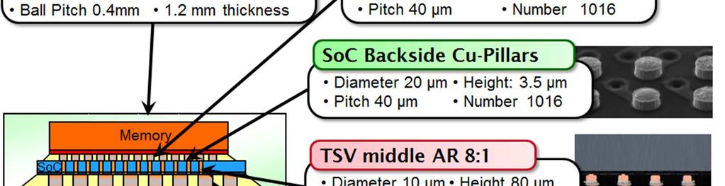
 3D SoC and Heterogeneous Integrations Content Introduction ST positioning Why 3D-Integration? CMOS Imager Sensor: the TSV success story! 3D SOC technology & applications Via Middle FE integrations Back-side
L évolution des architectures et des technologies d intégration des circuits intégrés dans les Data centers
 I N S T I T U T D E R E C H E R C H E T E C H N O L O G I Q U E L évolution des architectures et des technologies d intégration des circuits intégrés dans les Data centers 10/04/2017 Les Rendez-vous de
Monolithic 3D Integration using Standard Fab & Standard Transistors. Zvi Or-Bach CEO MonolithIC 3D Inc.
 Monolithic 3D Integration using Standard Fab & Standard Transistors Zvi Or-Bach CEO MonolithIC 3D Inc. 3D Integration Through Silicon Via ( TSV ), Monolithic Increase integration Reduce interconnect total
3D INTEGRATION, A SMART WAY TO ENHANCE PERFORMANCE. Leti Devices Workshop December 3, 2017
 3D INTEGRATION, A SMART WAY TO ENHANCE PERFORMANCE OVERAL GOAL OF THIS TALK Hybrid bonding 3D sequential 3D VLSI technologies (3D VIA Pitch
TechSearch International, Inc.
 On the Road to 3D ICs: Markets and Solutions E. Jan Vardaman President TechSearch International, Inc. www.techsearchinc.com High future cost of lithography Severe interconnect delay Noted in ITRS roadmap
Emerging IC Packaging Platforms for ICT Systems - MEPTEC, IMAPS and SEMI Bay Area Luncheon Presentation
 Emerging IC Packaging Platforms for ICT Systems - MEPTEC, IMAPS and SEMI Bay Area Luncheon Presentation Dr. Li Li Distinguished Engineer June 28, 2016 Outline Evolution of Internet The Promise of Internet
Interposer Technology: Past, Now, and Future
 Interposer Technology: Past, Now, and Future Shang Y. Hou TSMC 侯上勇 3D TSV: Have We Waited Long Enough? Garrou (2014): A Little More Patience Required for 2.5/3D All things come to those who wait In 2016,
Technology Platform Segmentation
 HOW TECHNOLOGY R&D LEADERSHIP BRINGS A COMPETITIVE ADVANTAGE FOR MULTIMEDIA CONVERGENCE Technology Platform Segmentation HP LP 2 1 Technology Platform KPIs Performance Design simplicity Power leakage Cost
Power dissipation! The VLSI Interconnect Challenge. Interconnect is the crux of the problem. Interconnect is the crux of the problem.
 The VLSI Interconnect Challenge Avinoam Kolodny Electrical Engineering Department Technion Israel Institute of Technology VLSI Challenges System complexity Performance Tolerance to digital noise and faults
Photon-to-Photon CMOS Imager: Opto-Electronic 3D Integration
 Photon-to-Photon CMOS Imager: Opto-Electronic 3D Integration Outline Key technologies for future CMOS imagers Bottlenecks for high speed imaging Our proposal Take home message Oct 12, 2017 Photon-to-Photon
High Volume Manufacturing Supply Chain Ecosystem for 2.5D HBM2 ASIC SiPs
 Open-Silicon.com 490 N. McCarthy Blvd, #220 Milpitas, CA 95035 408-240-5700 HQ High Volume Manufacturing Supply Chain Ecosystem for 2.5D HBM2 ASIC SiPs Open-Silicon Asim Salim VP Mfg. Operations 20+ experience
Addressable Test Chip Technology for IC Design and Manufacturing. Dr. David Ouyang CEO, Semitronix Corporation Professor, Zhejiang University 2014/03
 Addressable Test Chip Technology for IC Design and Manufacturing Dr. David Ouyang CEO, Semitronix Corporation Professor, Zhejiang University 2014/03 IC Design & Manufacturing Trends Both logic and memory
VLSI IMPLEMENTATION OF L2 MEMORY DESIGN FOR 3-D INTEGRATION G.Sri Harsha* 1, S.Anjaneeyulu 2
 ISSN 2277-2685 IJESR/June 2016/ Vol-6/Issue-6/150-156 G. Sri Harsha et. al., / International Journal of Engineering & Science Research VLSI IMPLEMENTATION OF L2 MEMORY DESIGN FOR 3-D INTEGRATION G.Sri
IMEC CORE CMOS P. MARCHAL
 APPLICATIONS & 3D TECHNOLOGY IMEC CORE CMOS P. MARCHAL OUTLINE What is important to spec 3D technology How to set specs for the different applications - Mobile consumer - Memory - High performance Conclusions
Technology and Manufacturing
 Technology and Manufacturing Executive Vice President Field Trip 2006 - London, May 23rd Field Trip 2006 - London, May 23rd Technology Technology Development Centers and Main Programs CMOS Logic Platform
Non-destructive, High-resolution Fault Imaging for Package Failure Analysis. with 3D X-ray Microscopy. Application Note
 Non-destructive, High-resolution Fault Imaging for Package Failure Analysis with 3D X-ray Microscopy Application Note Non-destructive, High-resolution Fault Imaging for Package Failure Analysis with 3D
Advanced Heterogeneous Solutions for System Integration
 Advanced Heterogeneous Solutions for System Integration Kees Joosse Director Sales, Israel TSMC High-Growth Applications Drive Product and Technology Smartphone Cloud Data Center IoT CAGR 12 17 20% 24%
Material technology enhances the density and the productivity of the package
 Material technology enhances the density and the productivity of the package May 31, 2018 Toshihisa Nonaka, Ph D. Packaging Solution Center Advanced Performance Materials Business Headquarter Hitachi Chemical
Soitec ultra-thin SOI substrates enabling FD-SOI technology. July, 2015
 Soitec ultra-thin SOI substrates enabling FD-SOI technology July, 2015 Agenda FD-SOI: Background & Value Proposition C1- Restricted July 8, 2015 2 Today Ultra-mobile & Connected Consumer At Any Time With
DEPARTMENT WAFER LEVEL SYSTEM INTEGRATION
 FRAUNHOFER INSTITUTE FOR RELIABILITY AND MICROINTEGRATION IZM DEPARTMENT WAFER LEVEL SYSTEM INTEGRATION ALL SILICON SYSTEM INTEGRATION DRESDEN ASSID ALL SILICON SYSTEM INTEGRATION DRESDEN FRAUNHOFER IZM-ASSID
Thermo Mechanical Modeling of TSVs
 Thermo Mechanical Modeling of TSVs Jared Harvest Vamsi Krishna ih Yaddanapudi di 1 Overview Introduction to Through Silicon Vias (TSVs) Advantages of TSVs over wire bonding in packages Role of TSVs in
3D technology for Advanced Medical Devices Applications
 3D technology for Advanced Medical Devices Applications By, Dr Pascal Couderc,Jerome Noiray, Dr Christian Val, Dr Nadia Boulay IMAPS MEDICAL WORKSHOP DECEMBER 4 & 5,2012 P.COUDERC 3D technology for Advanced
DFT-3D: What it means to Design For 3DIC Test? Sanjiv Taneja Vice President, R&D Silicon Realization Group
 I N V E N T I V E DFT-3D: What it means to Design For 3DIC Test? Sanjiv Taneja Vice President, R&D Silicon Realization Group Moore s Law & More : Tall And Thin More than Moore: Diversification Moore s
Comparison & highlight on the last 3D TSV technologies trends Romain Fraux
 Comparison & highlight on the last 3D TSV technologies trends Romain Fraux Advanced Packaging & MEMS Project Manager European 3D Summit 18 20 January, 2016 Outline About System Plus Consulting 2015 3D
3DIC & TSV interconnects business update
 3DIC & TSV interconnects business update ASET presentation. Infineon VTI Xilinx Synopsys Micron CEA LETI 2012 Copyrights Yole Developpement SA. All rights reserved. Fields of Expertise Yole Developpement
Advanced CSP & Turnkey Solutions. Fumio Ohyama Tera Probe, Inc.
 Advanced CSP & Turnkey Solutions Fumio Ohyama Tera Probe, Inc. Tera Probe - Corporate Overview 1. Company : Tera Probe, Inc. 2. Founded : August, 2005 3. Capital : Approx. USD118.2 million (as of March
Chapter 0 Introduction
 Chapter 0 Introduction Jin-Fu Li Laboratory Department of Electrical Engineering National Central University Jhongli, Taiwan Applications of ICs Consumer Electronics Automotive Electronics Green Power
Probing 25µm-diameter micro-bumps for Wide-I/O 3D SICs
 The International Magazine for the Semiconductor Packaging Industry Volume 18, Number 1 January February 2014 Probing 25µm-diameter micro-bumps for Wide-I/O 3D SICs Page 20 3D ICs The future of interposers
NoC Round Table / ESA Sep Asynchronous Three Dimensional Networks on. on Chip. Abbas Sheibanyrad
 NoC Round Table / ESA Sep. 2009 Asynchronous Three Dimensional Networks on on Chip Frédéric ric PétrotP Outline Three Dimensional Integration Clock Distribution and GALS Paradigm Contribution of the Third
3DIC & TSV interconnects
 3DIC & TSV interconnects 2012 Business update Semicon Taiwan 2012 baron@yole.fr Infineon VTI Xilinx Synopsys Micron CEA LETI 2012 Copyrights Yole Developpement SA. All rights reserved. Semiconductor chip
On GPU Bus Power Reduction with 3D IC Technologies
 On GPU Bus Power Reduction with 3D Technologies Young-Joon Lee and Sung Kyu Lim School of ECE, Georgia Institute of Technology, Atlanta, Georgia, USA yjlee@gatech.edu, limsk@ece.gatech.edu Abstract The
Advancing high performance heterogeneous integration through die stacking
 Advancing high performance heterogeneous integration through die stacking Suresh Ramalingam Senior Director, Advanced Packaging European 3D TSV Summit Jan 22 23, 2013 The First Wave of 3D ICs Perfecting
3D Embedded Multi-core: Some Perspectives
 3D Embedded Multi-core: Some Perspectives Fabien Clermidy, Florian Darve, Denis Dutoit, Walid Lafi, Pascal Vivet CEA-LETI, Minatec Campus, 38054 Grenoble, FRANCE {firstname.lastname@cea.fr} Abstract 3D
SMAFTI Package Technology Features Wide-Band and Large-Capacity Memory
 SMAFTI Package Technology Features Wide-Band and Large-Capacity Memory KURITA Yoichiro, SOEJIMA Koji, KAWANO Masaya Abstract and NEC Corporation have jointly developed an ultra-compact system-in-package
Moore s s Law, 40 years and Counting
 Moore s s Law, 40 years and Counting Future Directions of Silicon and Packaging Bill Holt General Manager Technology and Manufacturing Group Intel Corporation InterPACK 05 2005 Heat Transfer Conference
Heterogeneous Integration and the Photonics Packaging Roadmap
 Heterogeneous Integration and the Photonics Packaging Roadmap Presented by W. R. Bottoms Packaging Photonics for Speed & Bandwidth The Functions Of A Package Protect the contents from damage Mechanical
Japanese two Samurai semiconductor ventures succeeded in near 3D-IC but failed the business, why? and what's left?
 Japanese two Samurai semiconductor ventures succeeded in near 3D-IC but failed the business, why? and what's left? Liquid Design Systems, Inc CEO Naoya Tohyama Overview of this presentation Those slides
Five Emerging DRAM Interfaces You Should Know for Your Next Design
 Five Emerging DRAM Interfaces You Should Know for Your Next Design By Gopal Raghavan, Cadence Design Systems Producing DRAM chips in commodity volumes and prices to meet the demands of the mobile market
Packaging Technology for Image-Processing LSI
 Packaging Technology for Image-Processing LSI Yoshiyuki Yoneda Kouichi Nakamura The main function of a semiconductor package is to reliably transmit electric signals from minute electrode pads formed on
Multi-Die Packaging How Ready Are We?
 Multi-Die Packaging How Ready Are We? Rich Rice ASE Group April 23 rd, 2015 Agenda ASE Brief Integration Drivers Multi-Chip Packaging 2.5D / 3D / SiP / SiM Design / Co-Design Challenges: an OSAT Perspective
3D Hetero-Integration Technology for Future Automotive Smart Vehicle System
 3D Hetero-Integration Technology for Future Automotive Smart Vehicle System Kangwook Lee, Ph.D Professor, NICHe, Tohoku University Deputy Director, Global INTegration Initiative (GINTI) Kangwook Lee, Tohoku
Ultra-thin Capacitors for Enabling Miniaturized IoT Applications
 Ultra-thin Capacitors for Enabling Miniaturized IoT Applications Fraunhofer Demo Day, Oct 8 th, 2015 Konrad Seidel, Fraunhofer IPMS-CNT 10/15/2015 1 CONTENT Why we need thin passive devices? Integration
ECE520 VLSI Design. Lecture 1: Introduction to VLSI Technology. Payman Zarkesh-Ha
 ECE520 VLSI Design Lecture 1: Introduction to VLSI Technology Payman Zarkesh-Ha Office: ECE Bldg. 230B Office hours: Wednesday 2:00-3:00PM or by appointment E-mail: pzarkesh@unm.edu Slide: 1 Course Objectives
OPTICAL TECHNOLOGIES FOR TSV INSPECTION Arun A. Aiyer, Frontier Semiconductor 2127 Ringwood Ave, San Jose, California 95131
 OPTICAL TECHNOLOGIES FOR TSV INSPECTION Arun A. Aiyer, Frontier Semiconductor 2127 Ringwood Ave, San Jose, California 95131 ABSTRACT: In this paper, Frontier Semiconductor will introduce a new technology
The Evolution of Multi-Chip Packaging: from MCMs to 2.5/3D to Photonics. David McCann November 14, 2016
 The Evolution of Multi-Chip Packaging: from MCMs to 2.5/3D to Photonics David McCann November 14, 2016 Outline Multi-Chip Module Evolution We had MCM s. What Happened? What Have we Learned? Trends and
Thermal Modeling and Active Cooling
 Thermal Modeling and Active Cooling for 3D MPSoCs Prof. David Atienza, Embedded Systems Laboratory (ESL), EE Institute, Faculty of Engineering MPSoC 09, 2-7 August 2009 (Savannah, Georgia, USA) Thermal-Reliability
Wafer Level Packaging The Promise Evolves Dr. Thomas Di Stefano Centipede Systems, Inc. IWLPC 2008
 Wafer Level Packaging The Promise Evolves Dr. Thomas Di Stefano Centipede Systems, Inc. IWLPC 2008 / DEVICE 1.E+03 1.E+02 1.E+01 1.E+00 1.E-01 1.E-02 1.E-03 1.E-04 1.E-05 1.E-06 1.E-07 Productivity Gains
Advanced Packaging For Mobile and Growth Products
 Advanced Packaging For Mobile and Growth Products Steve Anderson, Senior Director Product and Technology Marketing, STATS ChipPAC Growing Needs for Silicon & Package Integration Packaging Trend Implication
3-D Package Integration Enabling Technologies
 3-D Package Integration Enabling Technologies Nanium - Semi Networking Day David Clark - Choon Heung Lee - Ron Huemoeller June 27th, 2013 Enabling a Microelectronic World Mobile Communications Driving
Challenges of Integration of Complex FHE Systems. Nancy Stoffel GE Global Research
 Challenges of Integration of Complex FHE Systems Nancy Stoffel GE Global Research Products drive requirements to sub-systems, components and electronics GE PRODUCTS CTQs: SWaP, $$, operating environment,
Packaging of Selected Advanced Logic in 2x and 1x nodes. 1 I TechInsights
 Packaging of Selected Advanced Logic in 2x and 1x nodes 1 I TechInsights Logic: LOGIC: Packaging of Selected Advanced Devices in 2x and 1x nodes Xilinx-Kintex 7XC 7 XC7K325T TSMC 28 nm HPL HKMG planar
Beyond Chip Stacking---Quilt Packaging Enabled 3D Systems
 Beyond Chip Stacking---Quilt Packaging Enabled 3D Systems Jason Kulick, President & Co-Founder jason.kulick@indianaic.com 574-217-4612 (South Bend, IN) May 3, 2016 2016 New England IMAPS Symposium Presentation
Opportunities & Challenges: 28nm & 2.5/3-D IC Design and Manufacturing
 Opportunities & Challenges: 28nm & 2.5/3-D IC Design and Manufacturing Vincent Tong Senior Vice President & Asia Pacific Executive Leader Copyright 2011 Xilinx Agenda Xilinx Business Drivers All in at
Package level Interconnect Options
 Package level Interconnect Options J.Balachandran,S.Brebels,G.Carchon, W.De Raedt, B.Nauwelaers,E.Beyne imec 2005 SLIP 2005 April 2 3 Sanfrancisco,USA Challenges in Nanometer Era Integration capacity F
BREAKING THE MEMORY WALL
 BREAKING THE MEMORY WALL CS433 Fall 2015 Dimitrios Skarlatos OUTLINE Introduction Current Trends in Computer Architecture 3D Die Stacking The memory Wall Conclusion INTRODUCTION Ideal Scaling of power
Introduction 1. GENERAL TRENDS. 1. The technology scale down DEEP SUBMICRON CMOS DESIGN
 1 Introduction The evolution of integrated circuit (IC) fabrication techniques is a unique fact in the history of modern industry. The improvements in terms of speed, density and cost have kept constant
Embedded Power Dies for System-in-Package (SiP)
") Embedded Power Dies for System-in-Package (SiP) D. Manessis, L. Boettcher, S. Karaszkiewicz, R.Patzelt, D. Schuetze, A. Podlasky, A. Ostmann Fraunhofer Institute for Reliability and Microintegration (IZM),
Embedded Power Dies for System-in-Package (SiP) D. Manessis, L. Boettcher, S. Karaszkiewicz, R.Patzelt, D. Schuetze, A. Podlasky, A. Ostmann Fraunhofer Institute for Reliability and Microintegration (IZM),
3D-IC is Now Real: Wide-IO is Driving 3D-IC TSV. Samta Bansal and Marc Greenberg, Cadence EDPS Monterey, CA April 5-6, 2012
 3D-IC is Now Real: Wide-IO is Driving 3D-IC TSV Samta Bansal and Marc Greenberg, Cadence EDPS Monterey, CA April 5-6, 2012 What the fuss is all about * Source : ECN Magazine March 2011 * Source : EDN Magazine
Embedded UTCP interposers for miniature smart sensors
 Embedded UTCP interposers for miniature smart sensors T. Sterken 1,2, M. Op de Beeck 2, Tom Torfs 2, F. Vermeiren 1,2, C. Van Hoof 2, J. Vanfleteren 1,2 1 CMST (affiliated with Ugent and IMEC), Technologiepark
EMERGING NON VOLATILE MEMORY
 EMERGING NON VOLATILE MEMORY Innovative components for neuromorphic architecture Leti, technology research institute Contact: leti.contact@cea.fr Neuromorphic architecture Brain-inspired computing has
edram to the Rescue Why edram 1/3 Area 1/5 Power SER 2-3 Fit/Mbit vs 2k-5k for SRAM Smaller is faster What s Next?
 edram to the Rescue Why edram 1/3 Area 1/5 Power SER 2-3 Fit/Mbit vs 2k-5k for SRAM Smaller is faster What s Next? 1 Integrating DRAM and Logic Integrate with Logic without impacting logic Performance,
Introduction. SK hynix
 It was very informative. I had a lot of questions answered. It was a good assembly of design and manufacturing elements. I learned a lot that I didn t know. It s good to hear that TSVs are ready for HBM.
Vertical Circuits. Small Footprint Stacked Die Package and HVM Supply Chain Readiness. November 10, Marc Robinson Vertical Circuits, Inc
 Small Footprint Stacked Die Package and HVM Supply Chain Readiness Marc Robinson Vertical Circuits, Inc November 10, 2011 Vertical Circuits Building Blocks for 3D Interconnects Infrastructure Readiness
PicoServer : Using 3D Stacking Technology To Enable A Compact Energy Efficient Chip Multiprocessor
 PicoServer : Using 3D Stacking Technology To Enable A Compact Energy Efficient Chip Multiprocessor Taeho Kgil, Shaun D Souza, Ali Saidi, Nathan Binkert, Ronald Dreslinski, Steve Reinhardt, Krisztian Flautner,
TSV Test. Marc Loranger Director of Test Technologies Nov 11 th 2009, Seoul Korea
 TSV Test Marc Loranger Director of Test Technologies Nov 11 th 2009, Seoul Korea # Agenda TSV Test Issues Reliability and Burn-in High Frequency Test at Probe (HFTAP) TSV Probing Issues DFT Opportunities
More Course Information
 More Course Information Labs and lectures are both important Labs: cover more on hands-on design/tool/flow issues Lectures: important in terms of basic concepts and fundamentals Do well in labs Do well
Thermal-Aware 3D IC Physical Design and Architecture Exploration
 Thermal-Aware 3D IC Physical Design and Architecture Exploration Jason Cong & Guojie Luo UCLA Computer Science Department cong@cs.ucla.edu http://cadlab.cs.ucla.edu/~cong Supported by DARPA Outline Thermal-Aware
There is a paradigm shift in semiconductor industry towards 2.5D and 3D integration of heterogeneous parts to build complex systems.
 Direct Connection and Testing of TSV and Microbump Devices using NanoPierce Contactor for 3D-IC Integration There is a paradigm shift in semiconductor industry towards 2.5D and 3D integration of heterogeneous
Intel: Driving the Future of IT Technologies. Kevin C. Kahn Senior Fellow, Intel Labs Intel Corporation
 Research @ Intel: Driving the Future of IT Technologies Kevin C. Kahn Senior Fellow, Intel Labs Intel Corporation kp Intel Labs Mission To fuel Intel s growth, we deliver breakthrough technologies that
Keynote Speaker. Matt Nowak Senior Director Advanced Technology Qualcomm CDMA Technologies
 Keynote Speaker Emerging High Density 3D Through Silicon Stacking (TSS) What s Next? Matt Nowak Senior Director Advanced Technology Qualcomm CDMA Technologies 8 Emerging High Density 3D Through Silicon
Gigascale Integration Design Challenges & Opportunities. Shekhar Borkar Circuit Research, Intel Labs October 24, 2004
 Gigascale Integration Design Challenges & Opportunities Shekhar Borkar Circuit Research, Intel Labs October 24, 2004 Outline CMOS technology challenges Technology, circuit and μarchitecture solutions Integration
VISUALIZING THE PACKAGING ROADMAP
 IEEE SCV EPS Chapter Meeting 3/13/2019 VISUALIZING THE PACKAGING ROADMAP IVOR BARBER CORPORATE VICE PRESIDENT, PACKAGING AMD IEEE EPS Lunchtime Presentation March 2019 1 2 2 www.cpmt.org/scv 3/27/2019
International Journal of Applied Sciences, Engineering and Management ISSN , Vol. 04, No. 05, September 2015, pp
 A Modular Shared L2 Memory Design for 3-D Integration P. Aparna 1, B. Kishore Kumar 2 1 Mtech Scholar, JB Institute of Engineering and Technology. Hyderabad. 2 Associate Professor, JB Institute of Engineering
Quilt Packaging For Power Electronics
 Quilt Packaging For Power Electronics 21 March 2013 Jason M. Kulick President, Co-Founder Indiana Integrated Circuits, LLC Overview Introduction Quilt Packaging (QP) technology Concept Examples Advantages
PSMC Roadmap For Integrated Photonics Manufacturing
 PSMC Roadmap For Integrated Photonics Manufacturing Richard Otte Promex Industries Inc. Santa Clara California For the Photonics Systems Manufacturing Consortium April 21, 2016 Meeting the Grand Challenges
2.5D interposer, 3DIC and TSV Interconnects Applications, market trends and supply chain evolutions
 2.5D interposer, 3DIC and TSV Interconnects Applications, market trends and supply chain evolutions Dr Lionel Cadix cadix@yole.fr CEA LETI Infineon VTI Synopsys Xilinx Micron 2012 Outline Introduction
Technology & Manufacturing. Laurent Bosson Executive Vice President Front End Technology & Manufacturing
 Technology & Manufacturing Laurent Bosson Executive Vice President Front End Technology & Manufacturing Manufacturing and Technology Strategy LEADING EDGE TECHNOLOGY + SHAREHOLDER VALUE TIME TO MARKET
SoC Memory Interfaces. Today and tomorrow at TSMC 2013 TSMC, Ltd
 SoC Memory Interfaces. Today and tomorrow at TSMC 2013 TSMC, Ltd 2 Agenda TSMC IP Ecosystem DDR Interfaces for SoCs Summary 3 TSMC Highlights Founded in 1987 The world's first dedicated semiconductor foundry
Stacking Untested Wafers to Improve Yield. The 3D Enigma
 Stacking Untested Wafers to Improve Yield or 3D: Where the Timid Go to Die The 3D Enigma The Promise High Performance Low Power Improved Density More than Moore or at least as much as Moore The Reality
Introduction. Summary. Why computer architecture? Technology trends Cost issues
 Introduction 1 Summary Why computer architecture? Technology trends Cost issues 2 1 Computer architecture? Computer Architecture refers to the attributes of a system visible to a programmer (that have
Innovative 3D Structures Utilizing Wafer Level Fan-Out Technology
 Innovative 3D Structures Utilizing Wafer Level Fan-Out Technology JinYoung Khim #, Curtis Zwenger *, YoonJoo Khim #, SeWoong Cha #, SeungJae Lee #, JinHan Kim # # Amkor Technology Korea 280-8, 2-ga, Sungsu-dong,
Industry Trends in 3D and Advanced Packaging
 Industry Trends in 3D and Advanced Packaging Outline Industry System and Component Challenges & Trends 3D and Advanced Packaging Value-proposition and Client Examples 3D Technology Details 3DIC / 3DTSV
Power Matters. TM. Why Embedded Die? Piers Tremlett Microsemi 22/9/ Microsemi Corporation. Company Proprietary 1
 Power Matters. TM Why Embedded Die? Piers Tremlett Microsemi 22/9/16 1 Introduction This presentation: Outlines our journey to make miniaturised SiP modules Compares : Embedded Die Technology (EDT) With