SECTION-A
|
|
|
- Julia Malone
- 5 years ago
- Views:
Transcription
1 M.Sc(CS) ( First Semester) Examination,2013 Digital Electronics Paper: Fifth SECTION-A I) An electronics circuit/ device which manipulates the operation on binary bits such as logical and arithemetic. It has one or more inputs and only one output used for making logical decision is called logic gates. Basic logic gates are AND, OR and NOT ii) Flip flops in its simplest form is known as latches. Latches are bistable device which can store either o or 1 binary bit. latches can be memory devices, and can store one bit of data for as long as the device is powered. iii) ( ) 2 =( ) 2 =(6 E. 8 A) 16 iv) ( 0.563)8 =. 5 X X X 8-3 V) PROM stands for Programmable Read only memory. It can be programmed once. EPROM stands for Erasable programmable memory. Content of this type of ROM can be altered electrically. vi) X X X 10 5 Vii) Drivers are the software which gives information or direct the operating system about how to interact with particular hardware devices. Example: Printer driver, CD driver, graphics adapter, sound card driver etc.
2 viii) ASCII code stands for American standard code for information inter change. It is a 7 bit code containing 128 characters. ASCII 65 is for the character A. basically ASCII codes are used for representing characters. ix) The Short comings of SR flip flop is the undetermined condition (input 11) is never used because its output is undetermined and the input 00 produces no change in the output. X) (5B.3A) 16 = ( ) 2 = ( ) 2 = ( )
3 SECTION-B 2. JK FLIP FLOP Fig. 2.5 shows one way to build a JK flip flop the variables J and K are called control inputs because they determine what the flip flop does on the arrival of a positive clock edge.
4 Inactiver: When J and K are both low, both AND gates are disabled and the circuit is inactive at all times including the rising edge of the clock. Reset : When J is low and K is high, the upper gate is disabled; so there is no way to set the flip - flop. The only possibility is reset. When Q is high, the lower gate passes a reset trigger as soon as the next positive clock edge arrives. This forces Q to become low. Therefore, J=0 and K=1 means that the next positive clock edge resets the flip-flop. Set: When J is high and K is low, the lower gate is disabled; So it is impossible to reset the flip-flop. But you can set the flip-flop as follows. When Q is low, Q is high; therefore, the upper gate passes a set trigger on the positive clock edge. This drives Q into the high state. That is, J=1 and K =0 means that the next positive clock edge sets the flip - flop. Toggle: When J and K both are high ( notice that this is the forbidden state with an RS flip - flop), it is possible to set or reset the flip - flop. If Q is high, the lower gate passes a reset trigger on the next positive clock edge. When Q is low, the upper gate passes a set trigger on the next positive clock edge. Either way Q changes to the compliment of the last state. Therefore, J =1 and K=1 means that the flip - flop will toggle on the next positive clock edge. ( toggle means switch to opposite state) Clocked RS flip flop Two different methods for constructing an RS flip flop were discussed in the previous section with NOR gate and NAND gate
5 realization. Both of these RS flip flops or latches, are said to be transparent ; that is any change in input at R or S is transmitted immediately to the output at Q and Q thus they acts as short term memory. It is possible to store or clock the flip flop in order to store information ( set it or reset it ) at any time, and then hold the stored information for any desired period of time. This flip flop is called clocked RS flip flop. The circuit of a clocked RS flip flop is shown in figure 2.6 with its symbol and truth table. Clocked RS flip flop x symbol and its truth table It consists of two additional and gates added at the input of R S flip flop. In addition to control inputs R and S, there is a clock input CK. The output of the two and circuits ( S 1 and R 1 ) will be 0 as long as CK = 0. then the state of the flip flop will remain unchanged and if S = 0, R = 1

 Y= ABD(C+C )+AC D (B+B )+A BC (D+D )+ABC D+AB CD =ABCD + ABC D + ABC D +AB C D +A")
6 3. i) then S = 0 R = 1 and the flip flop is reset to 0. On the other hand if S = 1, R = 0 then S =1 R = 1 and the flip flop is set to 1. the presence of R 1 =1 and S 1 =1, will however, results in an undetermined state ii) Y= ABD(C+C )+AC D (B+B )+A BC (D+D )+ABC D+AB CD =ABCD + ABC D + ABC D +AB C D +A BCD+A BC D + ABC D + AB CD (Any three differences of each)
7 Static RAM : 1. Used for cache memory. 2.Very cost effective. 3. Access time is faster 4. less storage space Dynamic Ram 1. Used for main memory 2. Cost is less than SRAM 3. Access time is less as compared to SRAM 4. Storage capability is high. Primary memory: 1. Access speed is high. 2. Less storage capacity. 3. Primary memories are internal memory. 4. May be volatile or non volatile. Secondary memory:1. Access speed is slow 2. High storage capacity 3. Secondary memories are external. 4. Secondary memories are non volatile memories. Main memory: 1. Storage capacity is high 2. High access speed
8 3.Constructed from DRAMs 4. Stores currently used data. Cache memory: 1. Storage capacity is low 2. low access speed 3. Constructed from SRAM 4. Stores frequently used data. Multiplexer: 1.It is a digital circuit which takes n input data line and selects one out of them or produces one output line. 2.Many input and one output. De multiplexer: 1.It is a digital circuit which takes one data input line and places the data on any of 2 n output lines. 2.One input line and many output line SEMICONDUCTOR MEMORIES Recent developments in semiconductor technology have provided a number or reliable and economical MSI and LSI memory circuits. The typical semiconductor memory consists of a rectangular array of memory cells. The basic memory cell is typically a transistor flip flop or a circuit capable of storing charge and used to store 1 bit of
9 information. The two general categories of semiconductor memories are RAM and ROM. They can be further divided into various types as illustrated as follows Memory Terminology: Read only memories come in four versions. The standard ROM is programmed by the manufacturer. The PROM can be programmed permanently by the user or manufacturer using special equipment. It can be programmed only once. The EPROM (Erasable Programmable Read Only Memory) can be programmed and erased by the user. Stored data in EPROM can be erased by passing high intensity ultraviolet light through a special transparent window in the top of the IC. Another erasable PROM is the EEPROM ( electrically Erasable Programmable Read Only Memory). The EEPROM can be erased and programmed by the user with special equipment. It is erased electrically rather than with ultraviolet light. All the types of ROM s
10 are non volatile light. All the types of ROM s area non volatile, which means they will not lose their data when power to the IC is turned off: PROMS AND EPROMS: The term ROM is generally reserved for memory chips that are programmed by the manufacturer. You have to send a list of data to be stored in the different memory locations to the manufacturer, who then produce a mask. Now the user can be able to read the stored. Data from the ROM. Programmable: A programmable ROM(PROM) is different. It allows the user to store the data. An instrument called a PROM programmer is used in storing the data( also called burning in ). once this has been done, the programming is permanent, that is the stored bits cannot be erased. Erasable: The erasable PROM(EPROM) used MOSFETs. Data is stored with a PROM programmer. Later, data can be erased with ultraviolet light passing through a window present on the top of memory chip. This releases stored charges and the effect is to wipe out the stored contents. The user can erase and store until the program and data are perfected. EEPROM: Another type of reprogrammable ROM device is the EEPROM (Electrically Erasable Read Only Memory). It is a non volatile like EPROM but does not require ultraviolet light to erase the data. It can be erased by using electrical pulses. It can be used for slower Semi conductor RAM s: Semiconductor RAMs may be static or

11 dynamic. Static RAM: Static RAM retain stored information only as long as the power supply is on. The static RAM uses bipolar or MOS flip flops. Static memory are cost effective. It consumes much power. they do not need re refreshing circuitry Dynamic RAM: A dynamic RAM may contain thousand of memory cells like this. The stored data must be refreshed ( Recharged) for every few milliseconds. Because the capacitor charge leaks off. Since memory cells than a static RAM of the same physical size. The disadvantage of dynamic RAM is the need to refresh the capacitor charge every few milliseconds. Dynamic RAMS are cheaper Figures for RAM and ROM Secondary memory with diagrams:
12 a Various types of codes (Any three) EBCDIC code : It is extended binary coded decimal interchange code. It is the standard character code for larger computer. It is an 8 bit code without parity. A ninth bit can be used for parity. With 8 its up to 256 characters can be coded. Gray codes: In gray codes there is only one bit changes at a time when a transition is made from one number to another: gray codes : 0000, 0001,0011, 0010,. Excess three codes: Excess three codes are unweighted codes. Ther are formed by adding three to a binary number. Excess three code of 4 is 4+3 = 7 Example : 101 (5) 1000 in excess three code. The ASCII code: To get information into and out of a computer, we need to use numbers, letters, and other symbols. This implies some kind of alphanumeric code for the I/O unit of a computer. At one time, every manufacturer had a different code, which led to all kinds of confusion. Eventually, industry settles on a input output code known as the American Standard code for Information Interchange (abbreviated ASCII). This code allows manufacturers, to standardize I/O hardware such as keyboards, Printers, video displays, and so on. It is a 7 bit code consisting of 128 characters.
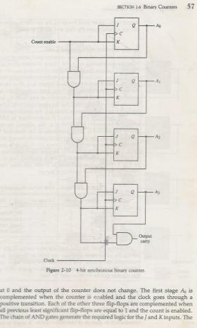
13 Ascii code also contains 8 bit including the parity bit. Other codes are BCD codes, Excess three codes b. 1. X+Y=Y+X 2. X.Y=Y.X 3. X(YZ)=(XY)Z=XYZ 4. X+XY=X 5. X(X+Y) =X 6. X(Y+Z)=XY+XZ 7. XY+XY =X 8. (X+Y)+Z=X+(Y+Z)=X+Y+Z 9. X+Y.Z = (X+Y)(X+Z) 10. (X+Y)(X+Y )=X b 4-Bit binary counter: A register that goes through a predetermined sequence of steps up on the application of input pulses is known as counters.a counter that follows binary sequence is called binary counter. A n bit counter is a register of n Flip flops and associated gates. A binary counter goes through the sequence of binary number 0000,0001, Every lower order bit is complemented after the next sequence. Ex- Binary count 0111 to 1000 is obtained by a) complementing the lower order bit b) complementing the second order bit because the first two bits of 0111 is 1 and complementing 4 th bit because all previous bits are 1 A 4 bit binary counter can be implemented by By using JK FF. JK FF has the property of toggling when the inpts are 11 and No change when
14 the inputs are 00. In addition the counter is controlled by using an enable input that turns the counter on or off. If the JK input is maintained at 00 there is no change in output. Wnen the enable input is 1 The lower order bit changes to 1 and rest of the bits doesnot change giving rise to the sequence The next clock pulses results
15 b

16 Registers: A register is a group of flip-flops capable of storing one bit of information. An n bit register has agroup of n flip-flop and capable of storing any binary information of n bits. 4 bit register consists of 4 D flip flops with common clock pulses. The clear input goes to special input of flip flops. When input goes to 0 all FFs reset. Clear input is used for clearing the register a. Digital Integrated Circuits:
17
18 8.b. Logic gates: Circuits used to process digital signals are called logic gates. Logic symbols are used to identify these circuits. They have one or more input signals but only one output signal. Gates are often called logic circuits because they can be analyzed with Boolean algebra As well as a standard Boolean Expression, the input and output information of any Logic Gate or circuit can be plotted into a table to give a visual representation of the switching function of the system and this is commonly called a Truth Table. A logic gate truth table shows each possible input combination to the gate or circuit with the resultant output depending upon the combination of these input(s). For example, consider a single 2-input logic circuit with input variables labeled as A and B. There are "four" possible input combinations or 2 2 of "OFF" and "ON" for the two inputs. However, when dealing with Boolean expressions and especially logic gate truth tables, we do not general use "ON" or "OFF" but instead give them bit values which represent a logic level "1" or a logic level "0" respectively. Then the four possible combinations of A and B for a 2-input logic gate is given as: Input Combination 1. - "OFF" - "OFF" or ( 0, 0 ) Input Combination 2. - "OFF" - "ON" or ( 0, 1 ) Input Combination 3. - "ON" - "OFF" or ( 1, 0 ) Input Combination 4. - "ON" - "ON" or ( 1, 1 ) Therefore, a 3-input logic circuit would have 8 possible input combinations or 2 3 and a 4-input logic circuit would have 16 or 2 4, and so on as the number of inputs increases. Then a logic circuit with "n" number of inputs would have 2 n possible input combinations of both "OFF" and "ON". In order
19 to keep things simple to understand, we will only deal with simple 2-input logic gates, but the principals are still the same for gates with more inputs. The Truth tables for a 2-input AND Gate, a 2-input OR Gate and a NOT Gate are given as: 2-input AND Gate For a 2-input AND gate, the output Q is true if BOTH input A "AND" input B are both true, giving the Boolean Expression of: ( Q = A and B ). Symbol Boolean Expression Q = A.B Truth Table A B Q Read as A AND B gives Q Note that the Boolean Expression for a two input AND gate can be written as: A.B or just simply AB without the decimal point. 2-input OR (Inclusive OR) Gate For a 2-input OR gate, the output Q is true if EITHER input A "OR" input B is true, giving the Boolean Expression of: ( Q = A or B ). Symbol Boolean Expression Q = A+B Truth Table A B Q Read as A OR B gives Q NOT Gate For a single input NOT gate, the output Q is ONLY true when the input is "NOT" true, the output is the inverse or complement of the input giving the Boolean Expression of: ( Q = NOT A ).
20 Symbol Truth Table A Q Boolean Expression Q = NOT A or A Read as inverse of A gives Q The NAND and the NOR Gates are a combination of the AND and OR Gates with that of a NOT Gate or inverter. 2-input NAND (Not AND) Gate For a 2-input NAND gate, the output Q is true if BOTH input A and input B are NOT true, giving the Boolean Expression of: ( Q = not(a and B) ). Symbol Boolean Expression Q = A.B Truth Table A B Q Read as A AND B gives NOT-Q 2-input NOR (Not OR) Gate For a 2-input NOR gate, the output Q is true if BOTH input A and input B are NOT true, giving the Boolean Expression of: ( Q = not(a or B) ). Symbol Boolean Expression Q = A+B Truth Table A B Q Read as A OR B gives NOT-Q
21 As well as the standard logic gates there are also two special types of logic gate function called an Exclusive-OR Gate and an Exclusive-NOR Gate. The actions of both of these types of gates can be made using the above standard gates however, as they are widely used functions, they are now available in standard IC form and have been included here as reference. 2-input EX-OR (Exclusive OR) Gate For a 2-input Ex-OR gate, the output Q is true if EITHER input A or if input B is true, but NOT both giving the Boolean Expression of: ( Q = (A and NOT B) or (NOT A and B) ). Symbol Boolean Expression Q = A B Truth Table A B Q input EX-NOR (Exclusive NOR) Gate For a 2-input Ex-NOR gate, the output Q is true if BOTH input A and input B are the same, either true or false, giving the Boolean Expression of: ( Q = (A and B) or (NOT A and NOT B) ). Symbol Boolean Expression Q = A B Truth Table A B Q Summary of all the 2-input Gates described above. The following Truth Table compares the logical functions of the 2-input logic gates above.
22 Inputs Truth Table Outputs for each Gate A B AND NAND OR NOR EX-OR EX-NOR The following table gives a list of the common logic functions and their equivalent Boolean notation. Logic Function Boolean Notation AND A.B OR A+B NOT A NAND A.B NOR A+B EX-OR (A.B) + (A.B) or A B EX-NOR (A.B) + or A B 2-input logic gate truth tables are given here as examples of the operation of each logic function, but there are many more logic gates with 3, 4 even 8 individual inputs. The multiple input gates are no different to the simple 2-input gates above, So a 4- input AND gate would still require ALL 4-inputs to be present to produce the required output at Q and its larger truth table would reflect that
Code No: R Set No. 1
 Code No: R059210504 Set No. 1 II B.Tech I Semester Supplementary Examinations, February 2007 DIGITAL LOGIC DESIGN ( Common to Computer Science & Engineering, Information Technology and Computer Science
Logic and Computer Design Fundamentals. Chapter 8 Memory Basics
 Logic and Computer Design Fundamentals Memory Basics Overview Memory definitions Random Access Memory (RAM) Static RAM (SRAM) integrated circuits Arrays of SRAM integrated circuits Dynamic RAM (DRAM) Read
MULTIMEDIA COLLEGE JALAN GURNEY KIRI KUALA LUMPUR
 STUDENT IDENTIFICATION NO MULTIMEDIA COLLEGE JALAN GURNEY KIRI 54100 KUALA LUMPUR SECOND SEMESTER FINAL EXAMINATION, 2013/2014 SESSION ITC2223 COMPUTER ORGANIZATION & ARCHITECTURE DSEW-E-F 1/13 18 FEBRUARY
PROGRAMMABLE LOGIC DEVICES
 PROGRAMMABLE LOGIC DEVICES Programmable logic devices (PLDs) are used for designing logic circuits. PLDs can be configured by the user to perform specific functions. The different types of PLDs available
M. Sc (CS) (II Semester) Examination, Subject: Computer System Architecture Paper Code: M.Sc-CS-203. Time: Three Hours] [Maximum Marks: 60
![M. Sc (CS) (II Semester) Examination, Subject: Computer System Architecture Paper Code: M.Sc-CS-203. Time: Three Hours] [Maximum Marks: 60](/thumbs/87/96339673.jpg "M. Sc (CS) (II Semester) Examination, Subject: Computer System Architecture Paper Code: M.Sc-CS-203. Time: Three Hours] [Maximum Marks: 60") M. Sc (CS) (II Semester) Examination, 2012-13 Subject: Computer System Architecture Paper Code: M.Sc-CS-203 Time: Three Hours] [Maximum Marks: 60 Note: Question Number 1 is compulsory. Answer any four
M. Sc (CS) (II Semester) Examination, 2012-13 Subject: Computer System Architecture Paper Code: M.Sc-CS-203 Time: Three Hours] [Maximum Marks: 60 Note: Question Number 1 is compulsory. Answer any four
Principles of Digital Techniques PDT (17320) Assignment No State advantages of digital system over analog system.
 Assignment No State advantages of digital system over analog system.") Assignment No. 1 1. State advantages of digital system over analog system. 2. Convert following numbers a. (138.56) 10 = (?) 2 = (?) 8 = (?) 16 b. (1110011.011) 2 = (?) 10 = (?) 8 = (?) 16 c. (3004.06)
Assignment No. 1 1. State advantages of digital system over analog system. 2. Convert following numbers a. (138.56) 10 = (?) 2 = (?) 8 = (?) 16 b. (1110011.011) 2 = (?) 10 = (?) 8 = (?) 16 c. (3004.06)
Injntu.com Injntu.com Injntu.com R16
 1. a) What are the three methods of obtaining the 2 s complement of a given binary (3M) number? b) What do you mean by K-map? Name it advantages and disadvantages. (3M) c) Distinguish between a half-adder
VALLIAMMAI ENGINEERING COLLEGE. SRM Nagar, Kattankulathur DEPARTMENT OF ELECTRONICS AND COMMUNICATION ENGINEERING EC6302 DIGITAL ELECTRONICS
 VALLIAMMAI ENGINEERING COLLEGE SRM Nagar, Kattankulathur-603 203 DEPARTMENT OF ELECTRONICS AND COMMUNICATION ENGINEERING EC6302 DIGITAL ELECTRONICS YEAR / SEMESTER: II / III ACADEMIC YEAR: 2015-2016 (ODD
Unit 6 1.Random Access Memory (RAM) Chapter 3 Combinational Logic Design 2.Programmable Logic
 Chapter 3 Combinational Logic Design 2.Programmable Logic") EE 200: Digital Logic Circuit Design Dr Radwan E Abdel-Aal, COE Unit 6.Random Access Memory (RAM) Chapter 3 Combinational Logic Design 2. Logic Logic and Computer Design Fundamentals Part Implementation
EE 200: Digital Logic Circuit Design Dr Radwan E Abdel-Aal, COE Unit 6.Random Access Memory (RAM) Chapter 3 Combinational Logic Design 2. Logic Logic and Computer Design Fundamentals Part Implementation
Lecture Objectives. Introduction to Computing Chapter 0. Topics. Numbering Systems 04/09/2017
 Lecture Objectives Introduction to Computing Chapter The AVR microcontroller and embedded systems using assembly and c Students should be able to: Convert between base and. Explain the difference between
END-TERM EXAMINATION
 (Please Write your Exam Roll No. immediately) END-TERM EXAMINATION DECEMBER 2006 Exam. Roll No... Exam Series code: 100919DEC06200963 Paper Code: MCA-103 Subject: Digital Electronics Time: 3 Hours Maximum
HANSABA COLLEGE OF ENGINEERING & TECHNOLOGY (098) SUBJECT: DIGITAL ELECTRONICS ( ) Assignment
 SUBJECT: DIGITAL ELECTRONICS ( ) Assignment") Assignment 1. What is multiplexer? With logic circuit and function table explain the working of 4 to 1 line multiplexer. 2. Implement following Boolean function using 8: 1 multiplexer. F(A,B,C,D) = (2,3,5,7,8,9,12,13,14,15)
Assignment 1. What is multiplexer? With logic circuit and function table explain the working of 4 to 1 line multiplexer. 2. Implement following Boolean function using 8: 1 multiplexer. F(A,B,C,D) = (2,3,5,7,8,9,12,13,14,15)
Code No: R Set No. 1
 Code No: R059210504 Set No. 1 II B.Tech I Semester Regular Examinations, November 2006 DIGITAL LOGIC DESIGN ( Common to Computer Science & Engineering, Information Technology and Computer Science & Systems
Presentation 4: Programmable Combinational Devices
 Presentation 4: Programmable Combinational Devices Asst. Prof Dr. Ahmet ÖZKURT DEUEEE Based on the Presentation by Prof. Kim, Young Ho Dept. of Information Computer Engineering E-mail : yhkim@hyowon.cs.pusan.ac.kr
Concept of Memory. The memory of computer is broadly categories into two categories:
 Concept of Memory We have already mentioned that digital computer works on stored programmed concept introduced by Von Neumann. We use memory to store the information, which includes both program and data.
Model EXAM Question Bank
 VELAMMAL COLLEGE OF ENGINEERING AND TECHNOLOGY, MADURAI Department of Information Technology Model Exam -1 1. List the main difference between PLA and PAL. PLA: Both AND and OR arrays are programmable
UNIT - V MEMORY P.VIDYA SAGAR ( ASSOCIATE PROFESSOR) Department of Electronics and Communication Engineering, VBIT
 Department of Electronics and Communication Engineering, VBIT") UNIT - V MEMORY P.VIDYA SAGAR ( ASSOCIATE PROFESSOR) contents Memory: Introduction, Random-Access memory, Memory decoding, ROM, Programmable Logic Array, Programmable Array Logic, Sequential programmable
UNIT - V MEMORY P.VIDYA SAGAR ( ASSOCIATE PROFESSOR) contents Memory: Introduction, Random-Access memory, Memory decoding, ROM, Programmable Logic Array, Programmable Array Logic, Sequential programmable
COLLEGE OF ENGINEERING DEPARTMENT OF ELECTRICAL AND ELECTRONICS ENGINEERING QUESTION BANK SUBJECT CODE & NAME: EC 1312 DIGITAL LOGIC CIRCUITS UNIT I
 KINGS COLLEGE OF ENGINEERING DEPARTMENT OF ELECTRICAL AND ELECTRONICS ENGINEERING QUESTION BANK SUBJECT CODE & NAME: EC 1312 DIGITAL LOGIC CIRCUITS YEAR / SEM: III / V UNIT I NUMBER SYSTEM & BOOLEAN ALGEBRA
Code No: 07A3EC03 Set No. 1
 Code No: 07A3EC03 Set No. 1 II B.Tech I Semester Regular Examinations, November 2008 SWITCHING THEORY AND LOGIC DESIGN ( Common to Electrical & Electronic Engineering, Electronics & Instrumentation Engineering,
Memory and Programmable Logic
 Memory and Programmable Logic Memory units allow us to store and/or retrieve information Essentially look-up tables Good for storing data, not for function implementation Programmable logic device (PLD),
Read and Write Cycles
 Read and Write Cycles The read cycle is shown. Figure 41.1a. The RAS and CAS signals are activated one after the other to latch the multiplexed row and column addresses respectively applied at the multiplexed
UNIT V (PROGRAMMABLE LOGIC DEVICES)
") UNIT V (PROGRAMMABLE LOGIC DEVICES) Introduction There are two types of memories that are used in digital systems: Random-access memory(ram): perform both the write and read operations. Read-only memory(rom):
UNIT V (PROGRAMMABLE LOGIC DEVICES) Introduction There are two types of memories that are used in digital systems: Random-access memory(ram): perform both the write and read operations. Read-only memory(rom):
B.Tech II Year I Semester (R13) Regular Examinations December 2014 DIGITAL LOGIC DESIGN
 Regular Examinations December 2014 DIGITAL LOGIC DESIGN") B.Tech II Year I Semester () Regular Examinations December 2014 (Common to IT and CSE) (a) If 1010 2 + 10 2 = X 10, then X is ----- Write the first 9 decimal digits in base 3. (c) What is meant by don
B.Tech II Year I Semester () Regular Examinations December 2014 (Common to IT and CSE) (a) If 1010 2 + 10 2 = X 10, then X is ----- Write the first 9 decimal digits in base 3. (c) What is meant by don
COMP2121: Microprocessors and Interfacing. Introduction to Microprocessors
 COMP2121: Microprocessors and Interfacing Introduction to Microprocessors http://www.cse.unsw.edu.au/~cs2121 Lecturer: Hui Wu Session 2, 2017 1 1 Contents Processor architectures Bus Memory hierarchy 2
Sense Amplifiers 6 T Cell. M PC is the precharge transistor whose purpose is to force the latch to operate at the unstable point.
 Announcements (Crude) notes for switching speed example from lecture last week posted. Schedule Final Project demo with TAs. Written project report to include written evaluation section. Send me suggestions
SHRI ANGALAMMAN COLLEGE OF ENGINEERING. (An ISO 9001:2008 Certified Institution) SIRUGANOOR, TIRUCHIRAPPALLI
 SIRUGANOOR, TIRUCHIRAPPALLI") SHRI ANGALAMMAN COLLEGE OF ENGINEERING AND TECHNOLOGY (An ISO 9001:2008 Certified Institution) SIRUGANOOR, TIRUCHIRAPPALLI 621 105 DEPARTMENT OF ELECTRONICS AND COMMUNICATION ENGINEERING EC1201 DIGITAL
SHRI ANGALAMMAN COLLEGE OF ENGINEERING AND TECHNOLOGY (An ISO 9001:2008 Certified Institution) SIRUGANOOR, TIRUCHIRAPPALLI 621 105 DEPARTMENT OF ELECTRONICS AND COMMUNICATION ENGINEERING EC1201 DIGITAL
CREATED BY M BILAL & Arslan Ahmad Shaad Visit:
 CREATED BY M BILAL & Arslan Ahmad Shaad Visit: www.techo786.wordpress.com Q1: Define microprocessor? Short Questions Chapter No 01 Fundamental Concepts Microprocessor is a program-controlled and semiconductor
8051 INTERFACING TO EXTERNAL MEMORY
 8051 INTERFACING TO EXTERNAL MEMORY Memory Capacity The number of bits that a semiconductor memory chip can store Called chip capacity It can be in units of Kbits (kilobits), Mbits (megabits), and so on
Lecture 13: Memory and Programmable Logic
 Lecture 13: Memory and Programmable Logic Syed M. Mahmud, Ph.D ECE Department Wayne State University Aby K George, ECE Department, Wayne State University Contents Introduction Random Access Memory Memory
II/IV B.Tech (Regular/Supplementary) DEGREE EXAMINATION. Answer ONE question from each unit.
 DEGREE EXAMINATION. Answer ONE question from each unit.") Hall Ticket Number: 14CS IT303 November, 2017 Third Semester Time: Three Hours Answer Question No.1 compulsorily. II/IV B.Tech (Regular/Supplementary) DEGREE EXAMINATION Common for CSE & IT Digital Logic
Hall Ticket Number: 14CS IT303 November, 2017 Third Semester Time: Three Hours Answer Question No.1 compulsorily. II/IV B.Tech (Regular/Supplementary) DEGREE EXAMINATION Common for CSE & IT Digital Logic
CS 320 February 2, 2018 Ch 5 Memory
 CS 320 February 2, 2018 Ch 5 Memory Main memory often referred to as core by the older generation because core memory was a mainstay of computers until the advent of cheap semi-conductor memory in the
Logic design Ibn Al Haitham collage /Computer science Eng. Sameer
 DEMORGAN'S THEOREMS One of DeMorgan's theorems stated as follows: The complement of a product of variables is equal to the sum of the complements of the variables. DeMorgan's second theorem is stated as
Code No: R Set No. 1
 Code No: R059210504 Set No. 1 II B.Tech I Semester Regular Examinations, November 2007 DIGITAL LOGIC DESIGN ( Common to Computer Science & Engineering, Information Technology and Computer Science & Systems
R07
 www..com www..com SET - 1 II B. Tech I Semester Supplementary Examinations May 2013 SWITCHING THEORY AND LOGIC DESIGN (Com. to EEE, EIE, BME, ECC) Time: 3 hours Max. Marks: 80 Answer any FIVE Questions
3. The high voltage level of a digital signal in positive logic is : a) 1 b) 0 c) either 1 or 0
 1 b) 0 c) either 1 or 0") 1. The number of level in a digital signal is: a) one b) two c) four d) ten 2. A pure sine wave is : a) a digital signal b) analog signal c) can be digital or analog signal d) neither digital nor analog
1. The number of level in a digital signal is: a) one b) two c) four d) ten 2. A pure sine wave is : a) a digital signal b) analog signal c) can be digital or analog signal d) neither digital nor analog
Hours / 100 Marks Seat No.
 17320 21718 3 Hours / 100 Seat No. Instructions (1) All Questions are Compulsory. (2) Answer each next main Question on a new page. (3) Figures to the right indicate full marks. (4) Assume suitable data,
DHANALAKSHMI SRINIVASAN COLLEGE OF ENGINEERING AND TECHNOLOGY
 DHANALAKSHMI SRINIVASAN COLLEGE OF ENGINEERING AND TECHNOLOGY Dept/Sem: II CSE/03 DEPARTMENT OF ECE CS8351 DIGITAL PRINCIPLES AND SYSTEM DESIGN UNIT I BOOLEAN ALGEBRA AND LOGIC GATES PART A 1. How many
Memory and Programmable Logic
 Memory and Programmable Logic Mano & Ciletti Chapter 7 By Suleyman TOSUN Ankara University Outline RAM Memory decoding Error detection and correction ROM Programmable Logic Array (PLA) Programmable Array
(ii) Simplify and implement the following SOP function using NOR gates:
 Simplify and implement the following SOP function using NOR gates:") DHANALAKSHMI COLLEGE OF ENGINEERING DEPARTMENT OF ELECTRONICS AND COMMUNICATION ENGINEERING EE6301 DIGITAL LOGIC CIRCUITS UNIT I NUMBER SYSTEMS AND DIGITAL LOGIC FAMILIES PART A 1. How can an OR gate be
DHANALAKSHMI COLLEGE OF ENGINEERING DEPARTMENT OF ELECTRONICS AND COMMUNICATION ENGINEERING EE6301 DIGITAL LOGIC CIRCUITS UNIT I NUMBER SYSTEMS AND DIGITAL LOGIC FAMILIES PART A 1. How can an OR gate be
Memory memories memory
 Memory Organization Memory Hierarchy Memory is used for storing programs and data that are required to perform a specific task. For CPU to operate at its maximum speed, it required an uninterrupted and
DIRECTORATE OF DISTANCE EDUCATION COMPUTER ORGANIZATION AND ARCHITECTURE/INTRODUCTION TO COMPUTER ORGANIZATION AND ARCHITECTURE
 www.lpude.in DIRECTORATE OF DISTANCE EDUCATION COMPUTER ORGANIZATION AND ARCHITECTURE/INTRODUCTION TO COMPUTER ORGANIZATION AND ARCHITECTURE Copyright 2012 Lovely Professional University All rights reserved
Memory Study Material
 Computer memory refers to the devices that are used to store data or programs on a temporary or permanent basis for use in a computer. Any data or instruction entered into the memory of a computer is considered
CONTENTS CHAPTER 1: NUMBER SYSTEM. Foreword...(vii) Preface... (ix) Acknowledgement... (xi) About the Author...(xxiii)
 Preface... (ix) Acknowledgement... (xi) About the Author...(xxiii)") CONTENTS Foreword...(vii) Preface... (ix) Acknowledgement... (xi) About the Author...(xxiii) CHAPTER 1: NUMBER SYSTEM 1.1 Digital Electronics... 1 1.1.1 Introduction... 1 1.1.2 Advantages of Digital Systems...
CONTENTS Foreword...(vii) Preface... (ix) Acknowledgement... (xi) About the Author...(xxiii) CHAPTER 1: NUMBER SYSTEM 1.1 Digital Electronics... 1 1.1.1 Introduction... 1 1.1.2 Advantages of Digital Systems...
Digital Logic Design Exercises. Assignment 1
 Assignment 1 For Exercises 1-5, match the following numbers with their definition A Number Natural number C Integer number D Negative number E Rational number 1 A unit of an abstract mathematical system
Dec Hex Bin ORG ; ZERO. Introduction To Computing
 Dec Hex Bin 0 0 00000000 ORG ; ZERO Introduction To Computing OBJECTIVES this chapter enables the student to: Convert any number from base 2, base 10, or base 16 to any of the other two bases. Add and
Computer Logical Organization Tutorial
 Computer Logical Organization Tutorial COMPUTER LOGICAL ORGANIZATION TUTORIAL Simply Easy Learning by tutorialspoint.com tutorialspoint.com i ABOUT THE TUTORIAL Computer Logical Organization Tutorial Computer
Memory Overview. Overview - Memory Types 2/17/16. Curtis Nelson Walla Walla University
 Memory Overview Curtis Nelson Walla Walla University Overview - Memory Types n n n Magnetic tape (used primarily for long term archive) Magnetic disk n Hard disk (File, Directory, Folder) n Floppy disks
Basic Organization Memory Cell Operation. CSCI 4717 Computer Architecture. ROM Uses. Random Access Memory. Semiconductor Memory Types
 CSCI 4717/5717 Computer Architecture Topic: Internal Memory Details Reading: Stallings, Sections 5.1 & 5.3 Basic Organization Memory Cell Operation Represent two stable/semi-stable states representing
Microcontroller Systems. ELET 3232 Topic 11: General Memory Interfacing
 Microcontroller Systems ELET 3232 Topic 11: General Memory Interfacing 1 Objectives To become familiar with the concepts of memory expansion and the data and address bus To design embedded systems circuits
Semiconductor Memories: RAMs and ROMs
 Semiconductor Memories: RAMs and ROMs Lesson Objectives: In this lesson you will be introduced to: Different memory devices like, RAM, ROM, PROM, EPROM, EEPROM, etc. Different terms like: read, write,
Programmable Logic Devices
 Programmable Logic Devices Programmable Logic Devices Fig. (1) General structure of PLDs Programmable Logic Device (PLD): is an integrated circuit with internal logic gates and/or connections that can
ELCT 912: Advanced Embedded Systems
 Advanced Embedded Systems Lecture 2: Memory and Programmable Logic Dr. Mohamed Abd El Ghany, Memory Random Access Memory (RAM) Can be read and written Static Random Access Memory (SRAM) Data stored so
R07. Code No: V0423. II B. Tech II Semester, Supplementary Examinations, April
 SET - 1 II B. Tech II Semester, Supplementary Examinations, April - 2012 SWITCHING THEORY AND LOGIC DESIGN (Electronics and Communications Engineering) Time: 3 hours Max Marks: 80 Answer any FIVE Questions
 Get Free notes at Module-I One s Complement: Complement all the bits.i.e. makes all 1s as 0s and all 0s as 1s Two s Complement: One s complement+1 SIGNED BINARY NUMBERS Positive integers (including zero)
THE MICROCOMPUTER SYSTEM CHAPTER - 2
 THE MICROCOMPUTER SYSTEM CHAPTER - 2 20 2.1 GENERAL ASPECTS The first computer was developed using vacuum tubes. The computers thus developed were clumsy and dissipating more power. After the invention
This tutorial gives a complete understanding on Computer Logical Organization starting from basic computer overview till its advanced architecture.
 About the Tutorial Computer Logical Organization refers to the level of abstraction above the digital logic level, but below the operating system level. At this level, the major components are functional
MEMORY BHARAT SCHOOL OF BANKING- VELLORE
 A memory is just like a human brain. It is used to store data and instructions. Computer memory is the storage space in computer where data is to be processed and instructions required for processing are
COMP3221: Microprocessors and. and Embedded Systems. Overview. Lecture 23: Memory Systems (I)
") COMP3221: Microprocessors and Embedded Systems Lecture 23: Memory Systems (I) Overview Memory System Hierarchy RAM, ROM, EPROM, EEPROM and FLASH http://www.cse.unsw.edu.au/~cs3221 Lecturer: Hui Wu Session
COMP3221: Microprocessors and Embedded Systems Lecture 23: Memory Systems (I) Overview Memory System Hierarchy RAM, ROM, EPROM, EEPROM and FLASH http://www.cse.unsw.edu.au/~cs3221 Lecturer: Hui Wu Session
Memory classification:- Topics covered:- types,organization and working
 Memory classification:- Topics covered:- types,organization and working 1 Contents What is Memory? Cache Memory PC Memory Organisation Types 2 Memory what is it? Usually we consider this to be RAM, ROM
R10. II B. Tech I Semester, Supplementary Examinations, May
 SET - 1 1. a) Convert the following decimal numbers into an equivalent binary numbers. i) 53.625 ii) 4097.188 iii) 167 iv) 0.4475 b) Add the following numbers using 2 s complement method. i) -48 and +31
CS 265. Computer Architecture. Wei Lu, Ph.D., P.Eng.
 CS 265 Computer Architecture Wei Lu, Ph.D., P.Eng. Part 4: Memory Organization Our goal: understand the basic types of memory in computer understand memory hierarchy and the general process to access memory
Hours / 100 Marks Seat No.
 17333 13141 3 Hours / 100 Seat No. Instructions (1) All Questions are Compulsory. (2) Answer each next main Question on a new page. (3) Illustrate your answers with neat sketches wherever necessary. (4)
 www.vidyarthiplus.com Question Paper Code : 31298 B.E./B.Tech. DEGREE EXAMINATION, NOVEMBER/DECEMBER 2013. Third Semester Computer Science and Engineering CS 2202/CS 34/EC 1206 A/10144 CS 303/080230012--DIGITAL
COA. Prepared By: Dhaval R. Patel Page 1. Q.1 Define MBR.
 Q.1 Define MBR. MBR( Memory buffer register) A Memory Buffer Register (MBR) is the register in a computers processor that stores the data being transferred to and from the devices It allowing the processor
Summer 2003 Lecture 18 07/09/03
 Summer 2003 Lecture 18 07/09/03 NEW HOMEWORK Instruction Execution Times: The 8088 CPU is a synchronous machine that operates at a particular clock frequency. In the case of the original IBM PC, that clock
Chapter 5 Internal Memory
 Chapter 5 Internal Memory Memory Type Category Erasure Write Mechanism Volatility Random-access memory (RAM) Read-write memory Electrically, byte-level Electrically Volatile Read-only memory (ROM) Read-only
KINGS COLLEGE OF ENGINEERING DEPARTMENT OF ELECTRICAL AND ELECTRONICS ENGINEERING QUESTION BANK NAME OF THE SUBJECT: EE 2255 DIGITAL LOGIC CIRCUITS
 KINGS COLLEGE OF ENGINEERING DEPARTMENT OF ELECTRICAL AND ELECTRONICS ENGINEERING QUESTION BANK NAME OF THE SUBJECT: EE 2255 DIGITAL LOGIC CIRCUITS YEAR / SEM: II / IV UNIT I BOOLEAN ALGEBRA AND COMBINATIONAL
DIGITAL SYSTEM FUNDAMENTALS (ECE421) DIGITAL ELECTRONICS FUNDAMENTAL (ECE4220. PROGRAMMABLE LOGIC DEVICES (PLDs)
 DIGITAL ELECTRONICS FUNDAMENTAL (ECE4220. PROGRAMMABLE LOGIC DEVICES (PLDs)") COURSE / CODE DIGITAL SYSTEM FUNDAMENTALS (ECE421) DIGITAL ELECTRONICS FUNDAMENTAL (ECE4220 PROGRAMMABLE LOGIC DEVICES (PLDs) A PLD, or programmable logic device, is an electronic component that is used
COURSE / CODE DIGITAL SYSTEM FUNDAMENTALS (ECE421) DIGITAL ELECTRONICS FUNDAMENTAL (ECE4220 PROGRAMMABLE LOGIC DEVICES (PLDs) A PLD, or programmable logic device, is an electronic component that is used
Organization. 5.1 Semiconductor Main Memory. William Stallings Computer Organization and Architecture 6th Edition
 William Stallings Computer Organization and Architecture 6th Edition Chapter 5 Internal Memory 5.1 Semiconductor Main Memory 5.2 Error Correction 5.3 Advanced DRAM Organization 5.1 Semiconductor Main Memory
MEMORY AND PROGRAMMABLE LOGIC
 MEMORY AND PROGRAMMABLE LOGIC Memory is a device where we can store and retrieve information It can execute a read and a write Programmable Logic is a device where we can store and retrieve information
William Stallings Computer Organization and Architecture 8th Edition. Chapter 5 Internal Memory
 William Stallings Computer Organization and Architecture 8th Edition Chapter 5 Internal Memory Semiconductor Memory The basic element of a semiconductor memory is the memory cell. Although a variety of
Memory. Outline. ECEN454 Digital Integrated Circuit Design. Memory Arrays. SRAM Architecture DRAM. Serial Access Memories ROM
 ECEN454 Digital Integrated Circuit Design Memory ECEN 454 Memory Arrays SRAM Architecture SRAM Cell Decoders Column Circuitry Multiple Ports DRAM Outline Serial Access Memories ROM ECEN 454 12.2 1 Memory
William Stallings Computer Organization and Architecture 6th Edition. Chapter 5 Internal Memory
 William Stallings Computer Organization and Architecture 6th Edition Chapter 5 Internal Memory Semiconductor Memory Types Semiconductor Memory RAM Misnamed as all semiconductor memory is random access
BHARATHIDASAN ENGINEERING COLLEGE Degree / Branch : B.E./ECE Year / Sem : II/ III Sub.Code / Name : EC6302/DIGITAL ELECTRONICS
 BHARATHIDASAN ENGINEERING COLLEGE Degree / Branch : B.E./ECE Year / Sem : II/ III Sub.Code / Name : EC6302/DIGITAL ELECTRONICS FREQUENTLY ASKED QUESTIONS UNIT I MINIMIZATION TECHNIQUES AND LOGIC GATES
INSTITUTE OF AERONAUTICAL ENGINEERING (Autonomous) Dundigal, Hyderabad
 Dundigal, Hyderabad") INSTITUTE OF AERONAUTICAL ENGINEERING (Autonomous) Dundigal, Hyderabad - 500 043 COMPUTER SCIENCE AND ENGINEERING TUTORIAL QUESTION BANK Name : DIGITAL LOGIC DESISN Code : AEC020 Class : B Tech III Semester
INSTITUTE OF AERONAUTICAL ENGINEERING (Autonomous) Dundigal, Hyderabad - 500 043 COMPUTER SCIENCE AND ENGINEERING TUTORIAL QUESTION BANK Name : DIGITAL LOGIC DESISN Code : AEC020 Class : B Tech III Semester
EECS150 Homework 2 Solutions Fall ) CLD2 problem 2.2. Page 1 of 15
 CLD2 problem 2.2. Page 1 of 15") 1.) CLD2 problem 2.2 We are allowed to use AND gates, OR gates, and inverters. Note that all of the Boolean expression are already conveniently expressed in terms of AND's, OR's, and inversions. Thus,
1.) CLD2 problem 2.2 We are allowed to use AND gates, OR gates, and inverters. Note that all of the Boolean expression are already conveniently expressed in terms of AND's, OR's, and inversions. Thus,
Computer Architecture: Part III. First Semester 2013 Department of Computer Science Faculty of Science Chiang Mai University
 Computer Architecture: Part III First Semester 2013 Department of Computer Science Faculty of Science Chiang Mai University Outline Decoders Multiplexers Registers Shift Registers Binary Counters Memory
Module 5a: Introduction To Memory System (MAIN MEMORY)
") Module 5a: Introduction To Memory System (MAIN MEMORY) R E F E R E N C E S : S T A L L I N G S, C O M P U T E R O R G A N I Z A T I O N A N D A R C H I T E C T U R E M O R R I S M A N O, C O M P U T E
Module 5a: Introduction To Memory System (MAIN MEMORY) R E F E R E N C E S : S T A L L I N G S, C O M P U T E R O R G A N I Z A T I O N A N D A R C H I T E C T U R E M O R R I S M A N O, C O M P U T E
Lecture-7 Characteristics of Memory: In the broad sense, a microcomputer memory system can be logically divided into three groups: 1) Processor
 Processor") Lecture-7 Characteristics of Memory: In the broad sense, a microcomputer memory system can be logically divided into three groups: 1) Processor memory 2) Primary or main memory 3) Secondary memory Processor
Lecture-7 Characteristics of Memory: In the broad sense, a microcomputer memory system can be logically divided into three groups: 1) Processor memory 2) Primary or main memory 3) Secondary memory Processor
Memory and Programmable Logic
 Digital Circuit Design and Language Memory and Programmable Logic Chang, Ik Joon Kyunghee University Memory Classification based on functionality ROM : Read-Only Memory RWM : Read-Write Memory RWM NVRWM
Computer Organization. 8th Edition. Chapter 5 Internal Memory
 William Stallings Computer Organization and Architecture 8th Edition Chapter 5 Internal Memory Semiconductor Memory Types Memory Type Category Erasure Write Mechanism Volatility Random-access memory (RAM)
VALLIAMMAI ENGINEERING COLLEGE
 VALLIAMMAI ENGINEERING COLLEGE SRM Nagar, Kattankulathur 603 203 DEPARTMENT OF INFORMATION TECHNOLOGY QUESTION BANK Academic Year 2018 19 III SEMESTER CS8351-DIGITAL PRINCIPLES AND SYSTEM DESIGN Regulation
Memory & Simple I/O Interfacing
 Chapter 10 Memory & Simple I/O Interfacing Expected Outcomes Explain the importance of tri-state devices in microprocessor system Distinguish basic type of semiconductor memory and their applications Relate
k -bit address bus n-bit data bus Control lines ( R W, MFC, etc.)
") THE MEMORY SYSTEM SOME BASIC CONCEPTS Maximum size of the Main Memory byte-addressable CPU-Main Memory Connection, Processor MAR MDR k -bit address bus n-bit data bus Memory Up to 2 k addressable locations
THE MEMORY SYSTEM SOME BASIC CONCEPTS Maximum size of the Main Memory byte-addressable CPU-Main Memory Connection, Processor MAR MDR k -bit address bus n-bit data bus Memory Up to 2 k addressable locations
Memories. Design of Digital Circuits 2017 Srdjan Capkun Onur Mutlu.
 Memories Design of Digital Circuits 2017 Srdjan Capkun Onur Mutlu http://www.syssec.ethz.ch/education/digitaltechnik_17 Adapted from Digital Design and Computer Architecture, David Money Harris & Sarah
Introduction read-only memory random access memory
 Memory Interface Introduction Simple or complex, every microprocessorbased system has a memory system. Almost all systems contain two main types of memory: read-only memory (ROM) and random access memory
An Overview of the Computer System. Kafui A. Prebbie 24
 An Overview of the Computer System Kafui A. Prebbie -kafui@kafui.com 24 The Parts of a Computer System What is a Computer? Hardware Software Data Users Kafui A. Prebbie -kafui@kafui.com 25 The Parts of
+1 (479)
") Memory Courtesy of Dr. Daehyun Lim@WSU, Dr. Harris@HMC, Dr. Shmuel Wimer@BIU and Dr. Choi@PSU http://csce.uark.edu +1 (479) 575-6043 yrpeng@uark.edu Memory Arrays Memory Arrays Random Access Memory Serial
Memory Courtesy of Dr. Daehyun Lim@WSU, Dr. Harris@HMC, Dr. Shmuel Wimer@BIU and Dr. Choi@PSU http://csce.uark.edu +1 (479) 575-6043 yrpeng@uark.edu Memory Arrays Memory Arrays Random Access Memory Serial
PART B. 3. Minimize the following function using K-map and also verify through tabulation method. F (A, B, C, D) = +d (0, 3, 6, 10).
 = +d (0, 3, 6, 10).") II B. Tech II Semester Regular Examinations, May/June 2015 SWITCHING THEORY AND LOGIC DESIGN (Com. to EEE, ECE, ECC, EIE.) Time: 3 hours Max. Marks: 70 Note: 1. Question Paper consists of two parts (Part-A
II B. Tech II Semester Regular Examinations, May/June 2015 SWITCHING THEORY AND LOGIC DESIGN (Com. to EEE, ECE, ECC, EIE.) Time: 3 hours Max. Marks: 70 Note: 1. Question Paper consists of two parts (Part-A
APPENDIX A SHORT QUESTIONS AND ANSWERS
 APPENDIX A SHORT QUESTIONS AND ANSWERS Unit I Boolean Algebra and Logic Gates Part - A 1. Define binary logic? Binary logic consists of binary variables and logical operations. The variables are designated
Aryan College. Computer Fundamental. Introduction to Computer System
 Computer Fundamental Unit 1 Introduction to Computer System 1. List various characteristics of computer. (2017) 2. Give name of two super computers. (2017) 3. What do you mean by system software? (2017)
MGU-BCA-205- Second Sem- Core VI- Fundamentals of Digital Systems- MCQ s. 2. Why the decimal number system is also called as positional number system?
 MGU-BCA-205- Second Sem- Core VI- Fundamentals of Digital Systems- MCQ s Unit-1 Number Systems 1. What does a decimal number represents? A. Quality B. Quantity C. Position D. None of the above 2. Why the
Computer Organization and Assembly Language (CS-506)
") Computer Organization and Assembly Language (CS-506) Muhammad Zeeshan Haider Ali Lecturer ISP. Multan ali.zeeshan04@gmail.com https://zeeshanaliatisp.wordpress.com/ Lecture 2 Memory Organization and Structure
Computer Organization and Assembly Language (CS-506) Muhammad Zeeshan Haider Ali Lecturer ISP. Multan ali.zeeshan04@gmail.com https://zeeshanaliatisp.wordpress.com/ Lecture 2 Memory Organization and Structure
Lecture (05) Boolean Algebra and Logic Gates
 Boolean Algebra and Logic Gates") Lecture (05) Boolean Algebra and Logic Gates By: Dr. Ahmed ElShafee ١ Minterms and Maxterms consider two binary variables x and y combined with an AND operation. Since eachv ariable may appear in either
Lecture (05) Boolean Algebra and Logic Gates By: Dr. Ahmed ElShafee ١ Minterms and Maxterms consider two binary variables x and y combined with an AND operation. Since eachv ariable may appear in either
Computer Arithematics Solved MCQs MCQs Multiple Choice Questions
 http://itbookshub.com/ Computer Arithematics Solved MCQs MCQs Multiple Choice Questions Computer Arithematics Solved MCQs 1) The advantage of single bus over a multi bus is? a. low cost b. flexibility
IT T35 Digital system desigm y - ii /s - iii
 UNIT - IV Sequential Logic II Memory and Programmable Logic: Random Access Memory memory decoding error detection and correction Read Only Memory Programmable Logic Arrays Programmable Array Logic. PRE-REQUISITE
Storage Elements & Sequential Circuits
 Storage Elements & Sequential Circuits LC-3 Data Path Revisited Now Registers and Memory 5-2 Combinational vs. Sequential Combinational Circuit always gives the same output for a given set of inputs Øex:
Overview. Memory Classification Read-Only Memory (ROM) Random Access Memory (RAM) Functional Behavior of RAM. Implementing Static RAM
 Random Access Memory (RAM) Functional Behavior of RAM. Implementing Static RAM") Memories Overview Memory Classification Read-Only Memory (ROM) Types of ROM PROM, EPROM, E 2 PROM Flash ROMs (Compact Flash, Secure Digital, Memory Stick) Random Access Memory (RAM) Types of RAM Static
Memories Overview Memory Classification Read-Only Memory (ROM) Types of ROM PROM, EPROM, E 2 PROM Flash ROMs (Compact Flash, Secure Digital, Memory Stick) Random Access Memory (RAM) Types of RAM Static
SIDDHARTH GROUP OF INSTITUTIONS :: PUTTUR Siddharth Nagar, Narayanavanam Road QUESTION BANK (DESCRIPTIVE)
") SIDDHARTH GROUP OF INSTITUTIONS :: PUTTUR Siddharth Nagar, Narayanavanam Road 517583 QUESTION BANK (DESCRIPTIVE) Subject with Code : STLD(16EC402) Year & Sem: II-B.Tech & I-Sem Course & Branch: B.Tech
SIDDHARTH GROUP OF INSTITUTIONS :: PUTTUR Siddharth Nagar, Narayanavanam Road 517583 QUESTION BANK (DESCRIPTIVE) Subject with Code : STLD(16EC402) Year & Sem: II-B.Tech & I-Sem Course & Branch: B.Tech
Review: Chip Design Styles
 MPT-50 Introduction to omputer Design SFU, Harbour entre, Spring 007 Lecture 9: Feb. 6, 007 Programmable Logic Devices (PLDs) - Read Only Memory (ROM) - Programmable Array Logic (PAL) - Programmable Logic