O N C A D E N C E V I R T U O S O. CHEN, Jason Application Engineer, Keysight Technologies
|
|
|
- Bernadette Lambert
- 5 years ago
- Views:
Transcription

1 O N C A D E N C E V I R T U O S O CHEN, Jason Application Engineer, Keysight Technologies
2 Introduction to Momentum Momentum Features for RFIC Design Circuit/EM Cosimulation Flow on Cadence Virtuoso Conclusion 2


3 3


4 Support Arbitrary Multi-layer structures High accuracy simulation for complex parasitics and EM coupling effects. Integrated in both ADS and Virtuoso Environment. Essential for passive components, patch antenna simulation and verification in RFIC, MMIC, PCB and RF modules. 4


5 ADS 201x Virtuoso IC / 6.x 3D Viewer BroadBand Spice Model Generator.subst.ltd 5

6 6


7 Lateral coupling Open Boundary Vertical coupling Vias Dielectric Layer1 Dielectric Layer2 Delectric Layers are extended to infinity Different materials on the same Z-coordination is not supported Arbitrary conductors crossing layers are not supported 7
8 S I D E W A L L C U R R E N T O F T H I C K C O N D U C T O R S Sidewall current flow, including vertical and horizontal, of thick metal is considered Top Bottom horizontal Sidewall vertical Sidewall horizontal ground plane Sidewall coupling effect can be simulated. 8


9 T H I C K C O N D U C T O R M O D E L Thick conductors can be analyzed in Momentum 3 Types of setting for Conductors 1. 3D Distributed Current densities of top, bottom and sidewall are all considered. Recommended Setting 2. 2D Distributed Only vertical current is considered at sidewall 3. Sheet Sidewall current is not considered Used for specific conditions Mesh shield GND Slow wave GND Patterned GND for eddy current reduction 9

10 V I A M O D E L 1. 3D Distributed Model Vertical and Horizontal current of vias are considered For high accuracy 2. 2D Distributed Model Vertical current of Vias are considered Recommended for IC. Usually via array is simplified to single via. There is no horizontal current of merged vias. 3. Lumped Model Vias are replaced with LR lumped model. Meshes are not generated for vias. Mutual inductance and self, mutual capacitance are not considered. 10
11 R F M O D E A N D M I C R O W A V E M O D E SPICE Momentum RF Momentum MW Spice model S parameters RF S parameters MW Frequency indep. L.... Frequency indep. C.... DC Conductor Loss(s).. DC Substrate Loss(s).. Loss tangent Skin Effect Substrate Surface Radiation Space Radiation MicroWave Mode=Full Wave RF Mode= Quasi-static 11
12 F R E Q U E N C Y R A N G E O F R F M O D E Limit of Layout Size (Space radiation can be ignored) D Dimension WaveLength 2 C light 2 Freq Limit of Substrate Stack-up (Surface radiation can be ignored) Freq [GHz] Thickness < 150 D [mm] Wavelength a (e r -1) The frequency range for RF mode will be shown in Status Window when running simulation. T e r a = 20 (with ground plane) a = 10 (without ground plane) Freq [GHz] < 300 a (e r -1) T [mm] 12

13 13
14 Cadence display.drf Support IC Interoperability Automatic Substrate Generation Metal Bias and Temperature Effect Layout Simplification Coilsys 14


15 ADS Layout Window Virtuoso Layout Window 15


16 Solving complex SiRF IC design challenges while working seamlessly of a single ADS / Virtuoso OA library Schematic and layout design optimization in ADS on OA library (EM & ETH-cosim, module and system level). Improved design efficiency and faster time to market while using RF-centric design tools at a competitive cost. Foundry PDK s & Rule Decks Forward looking nmdrc, nmlvs, PEX Calibre Interactive / Assura Schematic / Layout Virtuoso OA PDK + ADS callbacks & pcells Schematic / Layout ADS 2016 Virtuoso IC 6.1 CMOS SOI antenna switch Fan-out WLCSP Multi-technology PA module 16

 formats Similar to")

17 I T F & E N C R Y P T E D I R C X Automatic substrate generation for EM from foundry ICT (Cadence) and ITF (Synopsys) formats Similar to TSMC s ircx importer of ADS2016 Optionally generates Momentum module 17
 Metal bias tables specify the actual line width and spacing with respect to the drawn width and spacing With metal bias Without metal bias")
18 W I T H I T F O R I R C X EM simulation takes into account under/over etching of metal ircx and ITF files provide metal bias tables (GF and TSMC usually) Metal bias tables specify the actual line width and spacing with respect to the drawn width and spacing With metal bias Without metal bias 18


19 Momentum accounts for temperature-dependent conductor resistivity Substrate Editor Layout Simulation Circuit/EM Cosimulation 19
20 Computing Time Better accuracy, longer computing time Computing time is highly relative to number of meshes What s Mesh? Meshes are the divided elements of specific structures For larger layout, number of meshes also become larger For RFIC Although the layout size is small compared to wavelength, higher complexity leads to larger number of meshes. Layout simplification is required to reduce number of meshes without loss of accuracy 20

21 V I A A R R A Y Layout simplification for best speed and accuracy trade-off. Guidelines of Simplification Keep original layout of critical path If there are relatively thick and large ground patterns, current change on other pattern due to layout simplification is relatively small. GND Vias are used to make sure all GND patterns are at the same potential. Most current flow on thick metals and only few current flow in vias. It s better to merge Via array to single via. Via Merge Original Layout Simplified Layout 21
 Via Simplification Dummy Metal")
22 V I A A R R A Y Pcell is supported. Original layout is unchanged. Simplification is performed in background. The result of simplification can be checked and adjusted. Check in 3D viewer Display the simplified structure Pcell Can be adjust after check Simplified Model Simplification Setting (Stored in State) Via Simplification Dummy Metal Fill Option 22


23 V I A A R R A Y One more simplification method Number of meshes is less NEW Increment/clip to Lid Boundary 23
 For arbitrary metal fills 2. Metal Fill Presence 1. Assume is not existed if not drawn 2. Using layer purpose 3.")
24 M E T A L F I L L 1. Metal Fill Modeling Approach 1. Ignore 2. Equivalent dielectric constant (doesn t affect memory & simulation time) Assume metal fill is uniform 3. As original layout (memory consumption and simulation time is affected) For arbitrary metal fills 2. Metal Fill Presence 1. Assume is not existed if not drawn 2. Using layer purpose 3. Using pattern size 24

 are")
25 M E T A L F I L L M O D E L I N G Used when unrelated metal (=metal fill) are existed 25
26 M E T A L F I L L M O D E L I N G : R E M O V E U N R E L A T E D M E T A L Remove unrelated metal: Ignore metal fills The effect of metal fills are not considered. Metal fill layer 26


27 M E T A L F I L L M O D E L I N G : R E P L A C E D B Y E Q U I V A L E N T L A Y E R Replace by equivalent layer: change dielectric constant to equivalent value. Simulation time is the same. Metal Fill effect is considered Metal fill layer er: 3.9 XXX is calculated at the background. Related to Area fill fraction 27

28 M E T A L F I L L M O D E L I N G : K E E P U N R E L A T E D M E T A L Keep unrelated metal: solve metal fills as normal patterns. Use new algorism for unrelated metal. Less memory consumption and lower simulation time than previous version. 28


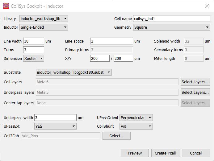
29 A U T O M A T I C I N D U C T O R D E S I G N E R 29

30 30
31 31

32 E M _ E X T R A C T E D V I E W G E N E R A T I O N Framework Virtuoso ADS Virtuoso Flow Create / Edit Top Design in Virtuoso Open in ADS Perform EM Partitioning Generate Views New Perform EM simulation Simulate in ADE New OA database Top Layout Top Layout Top EM Setup Top em_extracted Top_emcosim layout Top em_extracted Top_emcosim emmodel Top_emcosim emmodel Top_emcosim emmodel Express Pcell Plug-in Top_emcosim layout Express Pcell Plug-in 32
33 S T A R T F R O M V I R T U O S O L A Y O U T A N D O P E N I N A D S Top:layout in Virtuoso Top:layout* in ADS Layout and instance parameterization will be evaluated when the Top:layout express Pcells are created in Virtuoso or when ADS first uses the Top:layout view and they cannot be changed after that anymore. *Layout must be writeable if you need to edit the port setup 33

34 C R E A T E E M S E T U P V I E W A N D C O N F I G U R E T H E S E T U P Top:layout Top:emSetup Define partitioning E.g. 2 transistors and 2 mimcaps will be circuit-simulated Substrate, Simulation Options, Including proper ADS layer binding! Open the Port Editor and check/update the port definition Global scope added to override all port definitions Optionally modify the EM Model simulation setup 34
35 A U T O - C R E A T E T H E C O S I M U L A T I O N I T E M S After the user clicks Go, the following items will be auto-created: the auxiliary EM-modeling cell (Top_emCosim) with the proper CDF data the following views layout (Layout) emmodel (EM Model) spectre (symbol/cds simulation stop view) extra virtuoso cosimulation cell views: Top:emExtracted (Layout) 35


36 G E N E R A T E E M M O D E L D A T A Generate EM Model data Launch Momentum/FEM by clicking Evaluate model for default parameter values on the Database tab. Optionally included with cosimulation view creation to reduce number of clicks 36


37 T O P : E M _ E X T R A C T E D V I E W F O R S I M U L A T I O N This view can be the View for simulation in Cadence Similar to Assura-Virtuoso s av_extracted view. This auto-generated Layout view contains: The circuit-modeled component instances The em-modeled TopCell_emCosim instance The pins of TopCell:layout 37


38 R U N S I M U L A T I O N I N C A D E N C E A D E Instantiate the Top:symbol in a cadence testbench:schematic Run the simulation in ADE em_extracted must come upfront in the switch view list The EM Model view will be a stop view for spectre or GoldenGate 38
39 In this presentation, we have introduced Basics of Momentum Momentum Features for RFIC Design Circuit/EM cosimulation flow on Virtuoso With IC interoperability, users can choose Keysight solutions for advanced analyses, such as IC/Package EM simulation Electro-Thermal simulation System-Level analysis Useful tools in ADS (Loadpull, built-in display templates) 39
40
Joe Civello ADS Product Manager/ Keysight EEsof EDA
 Joe Civello 2018.01.11 ADS Product Manager/ Keysight EEsof EDA 3D Layout Viewing directly from the Layout Window 3D Editing & Routing PCB & IC/Module Design Dramatically Improved Visual Inspection Simplified
Outline. Darren Wang ADS Momentum P2
 Outline Momentum Basics: Microstrip Meander Line Momentum RF Mode: RFIC Launch Designing with Momentum: Via Fed Patch Antenna Momentum Techniques: 3dB Splitter Look-alike Momentum Optimization: 3 GHz Band
Using Sonnet in a Cadence Virtuoso Design Flow
 Using Sonnet in a Cadence Virtuoso Design Flow Purpose of this document: This document describes the Sonnet plug-in integration for the Cadence Virtuoso design flow, for silicon accurate EM modelling of
Chip/Package/Board Design Flow
 Chip/Package/Board Design Flow EM Simulation Advances in ADS 2011.10 1 EM Simulation Advances in ADS2011.10 Agilent EEsof Chip/Package/Board Design Flow 2 RF Chip/Package/Board Design Industry Trends Increasing
Introducing Virtuoso RF Designer (RFD) For RFIC Designs
 For RFIC Designs") A seminar on Cadence Virtuoso RF Designer is scheduled for March 5, 2008. To know more, write to Brajesh Heda at brajesh@cadence.com Introducing Virtuoso RF Designer (RFD) For RFIC Designs Introduction
A seminar on Cadence Virtuoso RF Designer is scheduled for March 5, 2008. To know more, write to Brajesh Heda at brajesh@cadence.com Introducing Virtuoso RF Designer (RFD) For RFIC Designs Introduction
Genesys 2012 Tutorial - Using Momentum Analysis for Microwave Planar Circuits
 Genesys 2012 Tutorial - Using Momentum Analysis for Microwave Planar Circuits Create the following schematics in Figure 1 with Genesys s schematic editor, which depicts two sections of a cascaded microstrip
Using Sonnet Interface in Eagleware-Elanix GENESYS. Sonnet Application Note: SAN-205A JULY 2005
 Using Sonnet Interface in Eagleware-Elanix GENESYS Sonnet Application Note: SAN-205A JULY 2005 Description of Sonnet Suites Professional Sonnet Suites Professional is an industry leading full-wave 3D Planar
Keysight EEsof EDA Planar Electromagnetic (EM) Simulation in ADS. Demo Guide
 Simulation in ADS. Demo Guide") Keysight EEsof EDA Planar Electromagnetic (EM) Simulation in ADS Demo Guide 02 Keysight Planar Electromagnetic (EM) Simulation in ADS - Demo Guide Keysight ADS provides two key electromagnetic simulators
Keysight EEsof EDA Planar Electromagnetic (EM) Simulation in ADS Demo Guide 02 Keysight Planar Electromagnetic (EM) Simulation in ADS - Demo Guide Keysight ADS provides two key electromagnetic simulators
TUTORIAL II ECE 555 / 755 Updated on September 11 th 2006 CADENCE LAYOUT AND PARASITIC EXTRACTION
 TUTORIAL II ECE 555 / 755 Updated on September 11 th 2006 CADENCE LAYOUT AND PARASITIC EXTRACTION After finishing a schematic of your design (Tutorial-I), the next step is creating masks which are for
Cadence Virtuoso Schematic Design and Circuit Simulation Tutorial
 Cadence Virtuoso Schematic Design and Circuit Simulation Tutorial Introduction This tutorial is an introduction to schematic capture and circuit simulation for ENGN1600 using Cadence Virtuoso. These courses
At Sonnet, we've been developing 3D planar high frequency EM software since 1983, and our software has earned a solid reputation as the world's most
 14.52 Rev 1.0 At Sonnet, we've been developing 3D planar high frequency EM software since 1983, and our software has earned a solid reputation as the world's most accurate commercial planar EM analysis
LAB EXERCISE 2 EM Basics (Momentum)
") ADS 2012 EM Basics (v2 April 2013) LAB EXERCISE 2 EM Basics (Momentum) Topics: EM simulation in ADS, focusing on Momentum, including substrate and port setups, 3D viewing, visualization, and more. Audience:
ADS 2012 EM Basics (v2 April 2013) LAB EXERCISE 2 EM Basics (Momentum) Topics: EM simulation in ADS, focusing on Momentum, including substrate and port setups, 3D viewing, visualization, and more. Audience:
AXIEM EM Simulation/Verification of a Cadence Allegro PCB
 Application Example AXIEM EM Simulation/Verification of a Cadence Allegro PCB Overview This application example outlines the electromagnetic (EM) simulation and verification flow that exists between Cadence
EDA Cloud ADS CIC EDA Cloud ADS Software User Manual
 EDA Cloud ADS CIC EDA Cloud ADS Software User Manual ADS www.cic.org.tw Ver.4.0 0 2016/11 1.0 EDA cloud ADS Flow 2.0 2015.08 2 EDA Cloud ADS EM 3.0 2015.12 2 EDA Cloud ADS EM A B C 2.0 2 3 3.1 2016.04
EM Analysis of High Frequency Printed Circuit Boards. Dr.-Ing. Volker Mühlhaus
 EM Analysis of High Frequency Printed Circuit Boards Dr.-Ing. Volker Mühlhaus volker@muehlhaus.com Agenda EM tools overview When to use EM analysis Application examples: Filters The importance of meshing
ESE 570 Cadence Lab Assignment 2: Introduction to Spectre, Manual Layout Drawing and Post Layout Simulation (PLS)
") ESE 570 Cadence Lab Assignment 2: Introduction to Spectre, Manual Layout Drawing and Post Layout Simulation (PLS) Objective Part A: To become acquainted with Spectre (or HSpice) by simulating an inverter,
ESE 570 Cadence Lab Assignment 2: Introduction to Spectre, Manual Layout Drawing and Post Layout Simulation (PLS) Objective Part A: To become acquainted with Spectre (or HSpice) by simulating an inverter,
EE434 ASIC & Digital Systems. From Layout to SPICE Simulation (Virtuoso, Calibre, HSpice) Spring 2017 Dae Hyun Kim
 Spring 2017 Dae Hyun Kim") EE434 ASIC & Digital Systems From Layout to SPICE Simulation (Virtuoso, Calibre, HSpice) Spring 2017 Dae Hyun Kim daehyun@eecs.wsu.edu 1 Preparation for Lab2 Download the following file into your working
EE434 ASIC & Digital Systems From Layout to SPICE Simulation (Virtuoso, Calibre, HSpice) Spring 2017 Dae Hyun Kim daehyun@eecs.wsu.edu 1 Preparation for Lab2 Download the following file into your working
Expert Layout Editor. Technical Description
 Expert Layout Editor Technical Description Agenda Expert Layout Editor Overview General Layout Editing Features Technology File Setup Multi-user Project Library Setup Advanced Programmable Features Schematic
Introduction to AWR Design Flow and New Features for V10
 Introduction to AWR Design Flow and New Features for V10 What s New In Version 10 imatch Matching Network Synthesis Matching Network Synthesis Tight integration with AWR tools Excellent starting point
Cadence IC Design Manual
 Cadence IC Design Manual For EE5518 ZHENG Huan Qun Lin Long Yang Revised on May 2017 Department of Electrical & Computer Engineering National University of Singapore 1 P age Contents 1 INTRODUCTION...
Amplifier Simulation Tutorial. Design Kit: Cadence 0.18μm CMOS PDK (gpdk180) (Cadence Version 6.1.5)
 (Cadence Version 6.1.5)") Amplifier Simulation Tutorial Design Kit: Cadence 0.18μm CMOS PDK (gpdk180) (Cadence Version 6.1.5) Yongsuk Choi, Marvin Onabajo This tutorial provides a quick introduction to the use of Cadence tools
Amplifier Simulation Tutorial Design Kit: Cadence 0.18μm CMOS PDK (gpdk180) (Cadence Version 6.1.5) Yongsuk Choi, Marvin Onabajo This tutorial provides a quick introduction to the use of Cadence tools
TQPED MMIC Design Training
 TQPED MMIC Design Training Outline Installation and Use of the Library AWR AWR Design Kit (PDK Process Design Kit) ICED Layout Kit Create a new document using the Library Environment Setup Hotkeys Background
Virtuoso Custom Design Platform GXL. Open Database. PDKs. Constraint Management. Customer IP
 Virtuoso Custom Design Platform GL The Cadence Virtuoso custom design platform is the industry s leading design system for complete front-to-back analog, RF, mixed-signal, and custom digital design. The
LAB EXERCISE 3B EM Techniques (Momentum)
") ADS 2012 EM Basics (v2 April 2013) LAB EXERCISE 3B EM Techniques (Momentum) Topics: EM options for meshing and the preprocessor, and using EM to simulate an inductor and use the model in schematic. Audience:
ADS 2012 EM Basics (v2 April 2013) LAB EXERCISE 3B EM Techniques (Momentum) Topics: EM options for meshing and the preprocessor, and using EM to simulate an inductor and use the model in schematic. Audience:
PDK-Based Analog/Mixed-Signal/RF Design Flow 11/17/05
 PDK-Based Analog/Mixed-Signal/RF Design Flow 11/17/05 Silvaco s What is a PDK? Which people build, use, and support PDKs? How do analog/mixed-signal/rf engineers use a PDK to design ICs? What is an analog/mixed-signal/rf
Integrating ADS into a High Speed Package Design Process
 Integrating ADS into a High Speed Package Design Process Page 1 Group/Presentation Title Agilent Restricted Month ##, 200X Agenda High Speed SERDES Package Design Requirements Performance Factor and Design
AWR. White Paper. Exactly How Electromagnetic Should Be Part of a Design Flow! introduction
 Extract Flow introduction Modern RF/microwave design flows make extensive use of electromagnetic (EM) analysis in many ways, and its co-existence and concurrency with circuit design and analysis can not
CVI_blink_cover Link to here
 CVI_blink_cover Link to here 14.52 Rev 1.0 At Sonnet, we've been developing 3D planar high frequency EM software since 1983, and our software has earned a solid reputation as the world's most accurate
A comprehensive workflow and methodology for parasitic extraction
 A comprehensive workflow and methodology for parasitic extraction Radoslav Prahov, Achim Graupner Abstract: In this paper is presented, analysed and assessed a design automation methodology of a tool employed
Efficient Meshing in Sonnet
 Efficient Meshing in Sonnet Purpose of this document: In this document, we will discuss efficient meshing in Sonnet, based on a wide variety of application examples. It will be shown how manual changes
Package on Board Simulation with 3-D Electromagnetic Simulation
 White Paper Package on Board Simulation with 3-D Electromagnetic Simulation For many years, designers have taken into account the effect of package parasitics in simulation, from using simple first-order
DEVELOPMENT OF PARAMETERIZED CELL OF SPIRAL INDUCTOR USING SKILL LANGUAGE
 DEVELOPMENT OF PARAMETERIZED CELL OF SPIRAL INDUCTOR USING SKILL LANGUAGE Vladimir Emilov Grozdanov 1, Diana Ivanova Pukneva 1, Marin Hristov Hristov 2 1 Smartcom, 7 th km, Tzarigradsko Chausee Blvd, 1784
m/matl - The EM Technology File Editor for RFIC
 m/matl - The EM Technology File Editor for RFIC Table of contents: m/matl - The EM Technology File Editor for RFIC... 1 1. Introduction... 2 2. What file formats and design flows are supported?... 2 Read
Microwave Office Training
 Microwave Office Training Schematic Layout Schematic Layout Schematic View Circuit We are Here! Schematic Layout View External World Need Export Mapping Two views of the same circuit! - including connectivity
Professor Muller Fall 2016 Sameet Ramakrishnan Eric Chang Adapted from prior EE140 and EE141 labs. EE 140/240A Lab 0 Full IC Design Flow
 Professor Muller Fall 2016 Sameet Ramakrishnan Eric Chang Adapted from prior EE140 and EE141 labs EE 140/240A Lab 0 Full IC Design Flow In this lab, you will walk through the full process an analog designer
CPE/EE 427, CPE 527, VLSI Design I: Tutorial #2, Schematic Capture, DC Analysis, Transient Analysis (Inverter, NAND2)
") CPE/EE 427, CPE 527, VLSI Design I: Tutorial #2, Schematic Capture, DC Analysis, Transient Analysis (Inverter, NAND2) Joel Wilder, Aleksandar Milenkovic, ECE Dept., The University of Alabama in Huntsville
CPE/EE 427, CPE 527, VLSI Design I: Tutorial #2, Schematic Capture, DC Analysis, Transient Analysis (Inverter, NAND2) Joel Wilder, Aleksandar Milenkovic, ECE Dept., The University of Alabama in Huntsville
Cadence Tutorial 2: Layout, DRC/LVS and Circuit Simulation with Extracted Parasitics
 Cadence Tutorial 2: Layout, DRC/LVS and Circuit Simulation with Extracted Parasitics Introduction This tutorial describes how to generate a mask layout in the Cadence Virtuoso Layout Editor. Use of DIVA
Chapter 4 Determining Cell Size
 Chapter 4 Determining Cell Size Chapter 4 Determining Cell Size The third tutorial is designed to give you a demonstration in using the Cell Size Calculator to obtain the optimal cell size for your circuit
HFSS 14 Update for SI and RF Applications Markus Kopp Product Manager, Electronics ANSYS, Inc.
 HFSS 14 Update for SI and RF Applications Markus Kopp Product Manager, Electronics ANSYS, Inc. 1 ANSYS, Inc. September 21, Advanced Solvers: Finite Arrays with DDM 2 ANSYS, Inc. September 21, Finite Arrays
An Overview of Standard Cell Based Digital VLSI Design
 An Overview of Standard Cell Based Digital VLSI Design With examples taken from the implementation of the 36-core AsAP1 chip and the 1000-core KiloCore chip Zhiyi Yu, Tinoosh Mohsenin, Aaron Stillmaker,
TABLE OF CONTENTS 1.0 PURPOSE INTRODUCTION ESD CHECKS THROUGHOUT IC DESIGN FLOW... 2
 TABLE OF CONTENTS 1.0 PURPOSE... 1 2.0 INTRODUCTION... 1 3.0 ESD CHECKS THROUGHOUT IC DESIGN FLOW... 2 3.1 PRODUCT DEFINITION PHASE... 3 3.2 CHIP ARCHITECTURE PHASE... 4 3.3 MODULE AND FULL IC DESIGN PHASE...
TSBCD025 High Voltage 0.25 mm BCDMOS
 TSBCD025 High Voltage 0.25 mm BCDMOS TSI Semiconductors' 0.25 mm process is a feature rich platform with best in class CMOS, LDMOS, and BiPolar devices. The BCD technology enables logic, Mixed-Signal,
AMS DESIGN METHODOLOGY
 OVER VIEW CADENCE ANALOG/ MIXED-SIGNAL DESIGN METHODOLOGY The Cadence Analog/Mixed-Signal (AMS) Design Methodology employs advanced Cadence Virtuoso custom design technologies and leverages silicon-accurate
UNIVERSITY OF WATERLOO
 UNIVERSITY OF WATERLOO UW ASIC DESIGN TEAM: Cadence Tutorial Description: Part I: Layout & DRC of a CMOS inverter. Part II: Extraction & LVS of a CMOS inverter. Part III: Post-Layout Simulation. The Cadence
RC Extraction. of an Inverter Circuit
 RC Extraction of an Inverter Circuit Santa Clara University Department of Electrical Engineering Under Guidance of Dr Samiha Mourad & Dr Shoba Krishnan Date of Last Revision: February 1, 2010 Copyright
Advanced Surface Based MoM Techniques for Packaging and Interconnect Analysis
 Electrical Interconnect and Packaging Advanced Surface Based MoM Techniques for Packaging and Interconnect Analysis Jason Morsey Barry Rubin, Lijun Jiang, Lon Eisenberg, Alina Deutsch Introduction Fast
Process technology and introduction to physical
 Neuromorphic Engineering II Lab 3, Spring 2014 1 Lab 3 March 10, 2014 Process technology and introduction to physical layout Today you will start to learn to use the Virtuoso layout editor XL which is
HIPEX Full-Chip Parasitic Extraction. Summer 2004 Status
 HIPEX Full-Chip Parasitic Extraction Summer 2004 Status What is HIPEX? HIPEX Full-Chip Parasitic Extraction products perform 3D-accurate and 2D-fast extraction of parasitic capacitors and resistors from
Lab 2. Standard Cell layout.
 Lab 2. Standard Cell layout. The purpose of this lab is to demonstrate CMOS-standard cell design. Use the lab instructions and the cadence manual (http://www.es.lth.se/ugradcourses/cadsys/cadence.html)
HFSS for ECAD: Package Modeling, MMIC and on-die extraction
 HFSS for ECAD: Package Modeling, MMIC and on-die extraction Alain Michel Technical Director, Europe 2010 ANSYS, Inc. All rights reserved. 1 ANSYS, Inc. Proprietary Agenda Introduction HFSS integrated Solver
Sonnet User s Guide Release 10
 Sonnet User s Guide Release 10 Cover: James Clerk Maxwell (1831-1879). A professor at Cambridge University, England, Maxwell established the interdependence of electricity and magnetism. In his classic
SONNET USER S GUIDE RELEASE 11
 SONNET USER S GUIDE RELEASE 11 Cover: James Clerk Maxwell (1831-1879). A professor at Cambridge University, England, Maxwell established the interdependence of electricity and magnetism. In his classic
Welcome. Joe Civello ADS Product Manager Agilent Technologies
 Welcome Joe Civello ADS Product Manager Agilent Technologies Agilent Technologies 2011 Agenda RF & microwave market trends & how Agilent EEsof is investing its R&D Multi-technology design with ADS 2011
Electromagnetic Compatibility ( EMC )
") Electromagnetic Compatibility ( EMC ) ESD Strategies in IC and System Design 8-1 Agenda ESD Design in IC Level ( ) Design Guide Lines CMOS Design Process Level Method Circuit Level Method Whole Chip Design
Electromagnetic Compatibility ( EMC ) ESD Strategies in IC and System Design 8-1 Agenda ESD Design in IC Level ( ) Design Guide Lines CMOS Design Process Level Method Circuit Level Method Whole Chip Design
Simulation and Modeling Techniques for Compact LTCC Packages
 Simulation and Modeling Techniques for Compact LTCC Packages Ted A. Miracco, Lloyd Nakamura, Malcolm Edwards Applied Wave Research, Inc. 1960 East Grand Avenue, Ste 430 El Segundo, CA 90245 Tel. 310-726-3000,
Hipex Full-Chip Parasitic Extraction
 What is Hipex? products perform 3D-accurate and 2D-fast extraction of parasitic capacitors and resistors from hierarchical layouts into hierarchical transistor-level netlists using nanometer process technology
High Speed and High Power Connector Design
 High Speed and High Power Connector Design Taiwan User Conference 2014 Introduction High speed connector: Electrically small Using differential signaling Data rate >100Mbps High power connector: Static
VLSI Lab Tutorial 3. Virtuoso Layout Editing Introduction
 VLSI Lab Tutorial 3 Virtuoso Layout Editing Introduction 1.0 Introduction The purpose of this lab tutorial is to guide you through the design process in creating a custom IC layout for your CMOS inverter
Sonnet s Cadence Virtuoso Interface Release 13 Update
 100 Elwood Davis Road North Syracuse, NY 13212 USA Sonnet s Cadence Virtuoso Interface Release 13 Update 2012 Sonnet Software, Inc. Sonnet is a registered trademark of Sonnet Software, Inc. Specialists
Extraction of Parasitic Capacitance and Resistances for HSPICE Simulation
 Extraction of Parasitic Capacitance and Resistances for HSPICE Simulation Make the layout window active and select Calibre > Run PEX from the top menu bar to start a Parasitic EXtraction. You will need
FACULTY OF ENGINEERING MULTIMEDIA UNIVERSITY LAB SHEET DIGITAL INTEGRATED CIRCUIT
 FACULTY OF ENGINEERING MULTIMEDIA UNIVERSITY LAB SHEET DIGITAL INTEGRATED CIRCUIT DIC1: Schematic Design Entry, Simulation & Verification DIC2: Schematic Driven Layout Drawing (SDL) Design Rule Check (DRC)
Silicon Creations and Calibre Ensuring Silicon Results will Match Circuit Simulation
 Silicon Creations and Calibre Ensuring Silicon Results will Match Circuit Simulation Andrew Cole VP, Silicon Creations Chris Clee Product Marketing Manager, Calibre Parasitic Extraction Products Agenda:
CS755 CAD TOOL TUTORIAL
 CS755 CAD TOOL TUTORIAL CREATING SCHEMATIC IN CADENCE Shi-Ting Zhou shi-ting@cs.wisc.edu After you have figured out what you want to design, and drafted some pictures and diagrams, it s time to input schematics
The Gold Standard for Parasitic Extraction and Signal Integrity Solutions
 The Gold Standard for Parasitic Extraction and Signal Integrity Solutions Critical Net Extraction and Analysis Full 3D seamless field solution High accuracy extraction Extracts net, tree, or entire path
Prepared by Dr. Ulkuhan Guler GT-Bionics Lab Georgia Institute of Technology
 Prepared by Dr. Ulkuhan Guler GT-Bionics Lab Georgia Institute of Technology OUTLINE Introduction Mapping for Schematic and Layout Connectivity Generate Layout from Schematic Connectivity Some Useful Features
Use of Symbolic Performance Models in Layout-Inclusive Synthesis of RF Low-Noise Amplifiers
 Use of Symbolic Performance Models in Layout-Inclusive Synthesis of RF Low-Noise Amplifiers Mukesh Ranjan, Amitava Bhaduri, Ranga Vemuri University of Cincinnati, Cincinnati, Ohio, USA. Wim Verhaegen,
Keysight EEsof EDA EMPro
 Keysight EEsof EDA EMPro 3D Electromagnetic Modeling and Simulation Environment Integrated with your ADS Design Flow Brochure Introduction Electromagnetic Professional (EMPro) is a 3D modeling and simulation
Circuits Multi Projets
 Circuits Multi Projets MPW Services Center for IC / MEMS Prototyping http://cmp.imag.fr Grenoble France CMP annual users meeting, 4 Feb. 2016, PARIS STMicroelectronics Standard Technology offers at CMP
CENG 4480 Lecture 11: PCB
 CENG 4480 Lecture 11: PCB Bei Yu Reference: Chapter 5 of Ground Planes and Layer Stacking High speed digital design by Johnson and Graham 1 Introduction What is a PCB Why we need one? For large scale production/repeatable
At Sonnet, we've been developing 3D planar high frequency EM software since 1983, and our software has earned a solid reputation as the world's most
 14.52 Rev 1.0 At Sonnet, we've been developing 3D planar high frequency EM software since 1983, and our software has earned a solid reputation as the world's most accurate commercial planar EM analysis
Creating the inv1 cell WITHOUT power pins
 Simulating with extracted parasitic Let s assume I designed the cell inv1, for which I created the views schematic, symbol and layout. Creating the inv1 cell WITHOUT power pins First, create the inverter
Solving the challenges posed by Chip/Package/Board Co-Design
 Solving the challenges posed by Chip/Package/Board Co-Design Identify and locate sources of unwanted coupling Simulation link to EM: Critical Interconnect, Vias, Discontinuities, Embedded Passives, etc
EE115C Digital Electronic Circuits. Tutorial 4: Schematic-driven Layout (Virtuoso XL)
") EE115C Digital Electronic Circuits Tutorial 4: Schematic-driven Layout (Virtuoso XL) This tutorial will demonstrate schematic-driven layout on the example of a 2-input NAND gate. Simple Layout (that won
EE115C Digital Electronic Circuits Tutorial 4: Schematic-driven Layout (Virtuoso XL) This tutorial will demonstrate schematic-driven layout on the example of a 2-input NAND gate. Simple Layout (that won
Sonnet is based in Syracuse, NY, USA with representatives across the globe.
 Getting Started At Sonnet, we've been developing 3D planar high frequency EM software since 1983, and our software has earned a solid reputation as the world's most accurate commercial planar EM analysis
ANALOG MICROELECTRONICS ( A)
") ANALOG MICROELECTRONICS (304-534A) IBM 130 nm CMOS Technology An Introduction to Cadence Virtuoso Layout Tool and the Analog Simulation Environment Prepared By - Azhar A. Chowdhury Updated by Ming Yang
ANALOG MICROELECTRONICS (304-534A) IBM 130 nm CMOS Technology An Introduction to Cadence Virtuoso Layout Tool and the Analog Simulation Environment Prepared By - Azhar A. Chowdhury Updated by Ming Yang
New paradigm for MEMS+IC Co-development
 New paradigm for MEMS+IC Co-development MEMS 진보된스마트세상을만듭니다. Worldwide First MEMS+IC Co-development Solution New paradigm for MEMS+IC Co-development A New Paradigm for MEMS+IC Development MEMS design
An Introduction to the Finite Difference Time Domain (FDTD) Method & EMPIRE XCcel
 Method & EMPIRE XCcel") An Introduction to the Finite Difference Time Domain (FDTD) Method & EMPIRE XCcel Simulation Model definition for FDTD DUT Port Simulation Box Graded Mesh six Boundary Conditions 1 FDTD Basics: Field components
An Introduction to the Finite Difference Time Domain (FDTD) Method & EMPIRE XCcel Simulation Model definition for FDTD DUT Port Simulation Box Graded Mesh six Boundary Conditions 1 FDTD Basics: Field components
CMOS Design Lab Manual
 CMOS Design Lab Manual Developed By University Program Team CoreEl Technologies (I) Pvt. Ltd. 1 Objective Objective of this lab is to learn the Mentor Graphics HEP2 tools as well learn the flow of the
Large-Scale Full-Wave Simulation
 Large-Scale Full-Wave Simulation Sharad Kapur and David Long Integrand Software, Inc. Areas of interest Consistent trends in IC design Increasing operating frequencies Modeling of passive structures (components,
Agilent 85194K IC-CAP BSIM4 Modeling Package
 Agilent 85194K IC-CAP BSIM4 Modeling Package Technical Overview The BSIM4 Modeling Package The BSIM4 Modeling Package offers a complete DC-to-RF CMOS modeling toolkit for U.C. Berkeley s BSIM4 model. Developed
Best practices for EMI filtering and IC bypass/decoupling applications
 X2Y Component Connection and PCB Layout Guidelines Best practices for EMI filtering and IC bypass/decoupling applications X2Y Attenuators, LLC 1 Common X2Y Circuit Uses EMI FILTERING Conducted and Radiated
EE 140/240A - Full IC Design Flow Tutorial
 Original document by Filip Maksimovic & Mike Lorek, Spring 2015, derived from earlier EE141 lab manuals Revisions for IC6 by David Burnett & Thaibao Phan, Spring 2016 Revisions made by Nandish Mehta to
0.35um design verifications
 0.35um design verifications Path end segment check (END) First check is the end segment check, This error is related to the routing metals when routing is done with a path. The finish of this path can
Electromagnetics. R14 Update. Greg Pitner ANSYS, Inc. February 24, 2012
 Electromagnetics R14 Update Greg Pitner 1 HFSS Version 14 2 HFSS Overview Advanced Integrated Solver Technologies Finite Arrays with Domain Decomposition Hybrid solving: FEBI, IE Regions Physical Optics
Understanding Strip (Finite) and Slot (Infinite) Ground based EM simulations in ADS
 and Slot (Infinite) Ground based EM simulations in ADS") Understanding Strip (Finite) and Slot (Infinite) Ground based EM simulations in ADS ADS offer three ways in which designers can model the return path (ground) for their structures to perform EM simulations.
Understanding Strip (Finite) and Slot (Infinite) Ground based EM simulations in ADS ADS offer three ways in which designers can model the return path (ground) for their structures to perform EM simulations.
ECE471/571 Energy Efficient VLSI Design Project 2 Cadence Setup and Creation of an Inverter Due Date 11:30 am on Friday, February 2 nd, 2018
 ECE471/571 Energy Efficient VLSI Design Project 2 Cadence Setup and Creation of an Inverter Due Date 11:30 am on Friday, February 2 nd, 2018 Introduction This project will first walk you through the setup
take control of your photonics design flow Photonic-Electronic IC design and implementation Pieter Dumon 27/09/2016
 take control of your photonics design flow Photonic-Electronic IC design and implementation Pieter Dumon 27/09/2016 Giving photonic IC designers the same power as electronic IC designers. Make it possible
Chapter 7 Agilent Interface Tutorial
 Chapter 7 Agilent Interface Tutorial Chapter 7 Agilent Interface Tutorial This tutorial provides you with an overview of the basic use of the Agilent Interface. For a detailed discussion of the Agilent
THERMAL GRADIENT AND IR DROP AWARE DESIGN FLOW FOR ANALOG-INTENSIVE ASICS
 THERMAL GRADIENT AND IR DROP AWARE DESIGN FLOW FOR ANALOG-INTENSIVE ASICS Pacific MicroCHIP Corp. AIMS-CAT November, 2009 OUTLINE Motivation Thermal Gradient Impact Simulation Methodology Results Accurate
Columbia Univerity Department of Electrical Engineering Fall, 2004
 Columbia Univerity Department of Electrical Engineering Fall, 2004 Course: EE E4321. VLSI Circuits. Instructor: Ken Shepard E-mail: shepard@ee.columbia.edu Office: 1019 CEPSR Office hours: MW 4:00-5:00
At Sonnet, we've been developing 3D planar high frequency EM software since 1983, and our software has earned a solid reputation as the world's most
 14.52 Rev 1.0 At Sonnet, we've been developing 3D planar high frequency EM software since 1983, and our software has earned a solid reputation as the world's most accurate commercial planar EM analysis
Physical Implementation
 CS250 VLSI Systems Design Fall 2009 John Wawrzynek, Krste Asanovic, with John Lazzaro Physical Implementation Outline Standard cell back-end place and route tools make layout mostly automatic. However,
Concurrent, OA-based Mixed-signal Implementation
 Concurrent, OA-based Mixed-signal Implementation Mladen Nizic Eng. Director, Mixed-signal Solution 2011, Cadence Design Systems, Inc. All rights reserved worldwide. Mixed-Signal Design Challenges Traditional
Mentor Graphics VLSI CAD Tutorials
 VLSI Design Flow Using Mentor-Graphics Tools Mentor Graphics VLSI CAD Tutorials School of Engineering Santa Clara University Santa Clara, CA 95053 At the Design Center, School of Engineering, of Santa
Virtuoso Layout Editor
 This tutorial will cover the basic steps involved in using the Cadence layout editor called Virtuoso, extracting layout, and running simulation on the layout. The inverter layout is used as an example
CS/EE 5720/6720 Analog IC Design Tutorial for Schematic Design and Analysis using Spectre
 CS/EE 5720/6720 Analog IC Design Tutorial for Schematic Design and Analysis using Spectre Introduction to Cadence EDA: The Cadence toolset is a complete microchip EDA (Electronic Design Automation) system,
Design rule illustrations for the AMI C5N process can be found at:
 Cadence Tutorial B: Layout, DRC, Extraction, and LVS Created for the MSU VLSI program by Professor A. Mason and the AMSaC lab group. Revised by C Young & Waqar A Qureshi -FS08 Document Contents Introduction
SOI REQUIRES BETTER THAN IR-DROP. F. Clément, CTO
 SOI REQUIRES BETTER THAN IR-DROP F. Clément, CTO Content IR Drop Vs. System-level Interferences CWS Expertise Accuracy and Performance Silicon Validation Conclusion Copyright CWS 2004-2016 2 Sensitive
Latch-Up. Parasitic Bipolar Transistors
 Latch-Up LATCH-UP CIRCUIT Latch-up is caused by an SCR (Silicon Controlled Rectifier) circuit. Fabrication of CMOS integrated circuits with bulk silicon processing creates a parasitic SCR structure. The
APPENDIX-A INTRODUCTION TO OrCAD PSPICE
 220 APPENDIX-A INTRODUCTION TO OrCAD PSPICE 221 APPENDIX-A INTRODUCTION TO OrCAD PSPICE 1.0 INTRODUCTION Computer aided circuit analysis provides additional information about the circuit performance that