Silicon Photonics Scalable Design Framework:
|
|
|
- Harvey Butler
- 5 years ago
- Views:
Transcription


1 Silicon Photonics Scalable Design Framework: From Design Concept to Physical Verification Hossam Sarhan Technical Marketing Engineer

2 Objective: Scalable Photonics Design Infrastructure The electronic IC market has benefitted greatly from the scalability attributed to Moore s Law Meanwhile the photonic market remains limited to relatively small circuits Design differentiation still focused on device physics as opposed to novel device and sub-circuit re-use. 31 March 2017 Hossam Sarhan / Mentor Graphics 2
3 What is Required to Move Forward? Scalable Design Tools Large scale optical simulation based on compact models Automated/semi-automated layout Physical verification and DFM Dedicated Process Development Kits (PDKs) Pre-characterized compact models Pre-characterized device pcells Process specific PV and DFM decks Validated tool settings Reference Flows Validated design flows Device characterization procedures Test and measurement methodologies Validated Re-Usable IP? 31 March 2017 Hossam Sarhan / Mentor Graphics 3


4 Partnering to provide IoT Solutions 31 March 2017 Hossam Sarhan / Mentor Graphics 4

5 Mentor s Custom IC Design Tools Joint support for Pyxis and Tanner EDA Products Both utilize common PDK development utilities Supports Python based PCells Supports OA based PDK development Both support interface to Mentors enterprise level simulation and verification tools Full support for Calibre Physical Verification tools Full support for Eldo Platform with Verilog-A support Tanner EDA will be fully OA native this year L-Edit is Open Access native S-Edit will be Open Access native in 17.2 release 31 March 2017 Hossam Sarhan / Mentor Graphics 5

6 Mentor s Photonic IC Design Flow Calibre s Scalability with Tanner EDA platform 31 March 2017 Hossam Sarhan / Mentor Graphics 6

7 Mentor s Photonic IC Design Flow Customer Driven 31 March 2017 Hossam Sarhan / Mentor Graphics 7
8 Physical Verification Challenges Rendered Curves Results in False DRC Errors Difficulty in LVS Device Recognition and Optical Property Comparison Need to Pass Waveguide Interconnect Extraction to Post-Layout Simulation Mask Generation and Silicon Manufacture Varies from Design Intent 31 March 2017 Hossam Sarhan / Mentor Graphics 8
9 DRC FOR NON-MANHATTAN PHOTONIC DESIGNS
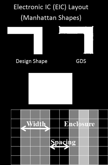
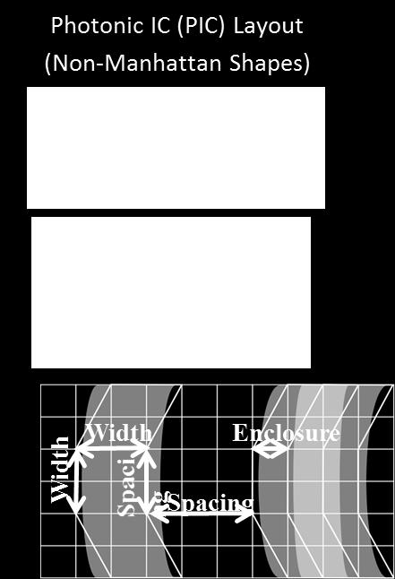
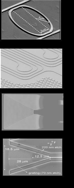

10 DRC on Si-Photonics Components 31 March 2017 Hossam Sarhan / Mentor Graphics 10
 Concentric arcs: Fabrication constraint :")


11 Addressing DRC Photonics Challenges I. False Error Induced by grid Snapping (1/2) Concentric arcs: Fabrication constraint : Width > 1 µm, Space > 1 µm Error_width := width < 1 µm Error_space := space < 1 µm Traditional DRC Check Concentric Arcs components Number of Violations = 1500 Concentric Arcs with DRC violations Silicon Photonics Design Rule Checking:Application of a Programmable Modeling Engine for Non-Manhattan Geometry Verification, presented at VLSI-SoC March 2017 Hossam Sarhan / Mentor Graphics 11
 Concentric arcs: Fabrication constraint : Width > 1 µm, Space > 1 µm Error_width := width < 1 µm Error_space := space < 1 µm Traditional DRC Check New DRC")
 < (1 -tol*) µm Else: Error_rod_width := Width(rod) < max_width µm *.")
12 Addressing DRC Photonics Challenges I. False Error Induced by grid Snapping (2/2) Concentric arcs: Fabrication constraint : Width > 1 µm, Space > 1 µm Error_width := width < 1 µm Error_space := space < 1 µm Traditional DRC Check New DRC Check using Calibre EqDRC All_Thin_rod := Width (rod) < 1 µm W = Width (Thin_rod_width) α = Angle (Thin_rod_width) L = Length (thin_rod_width) If (0 < α < max_angle) OR (L < max_length) Then: Error_rod_width := Width(rod) < (1 -tol*) µm Else: Error_rod_width := Width(rod) < max_width µm *.tol tolerance determined by applying tolerance factor according to fabrication grids and DRC rounding factors. (2sqrt(2). Grid) Number of Violations = 1500 Number of Violations = 145 Concentric Arcs with DRC violations Silicon Photonics Design Rule Checking:Application of a Programmable Modeling Engine for Non-Manhattan Geometry Verification, presented at VLSI-SoC 2014 DRC Post Processing using EqDRC capabilities 31 March 2017 Hossam Sarhan / Mentor Graphics 12
13 Addressing DRC Photonics Challenges II. Enable Multi-Dimensional Check (1/2) Taper test structure Taper is a trapezoidal shape. End width (w) varies from.05 to 1 µm Fabrication constraint : Line width > 1 µm For Robust strip design : relaxed width constraint with increased angle 1 µm.8 µm.8µm Space error DRC width Error <.1µm 31 March 2017 Hossam Sarhan / Mentor Graphics 13
 Traditional DRC Rule (Complicated and non accurate) EqDRC Rule (Simple and")
 α critical = f(width(rod)) Thin_rod := α c /α >1 Space error DRC")
14 Addressing DRC Photonics Challenges II. Enable Multi-Dimensional Check (2/2) Traditional DRC Rule (Complicated and non accurate) EqDRC Rule (Simple and Accurate) Error_Width_1 := width < w1 when 0 < α < α 1 Error_Width_2 := width < w2 when α 1 < α < α 2 Error_Width_3 := width < w3 when α 2 < α < α 3 α = Angle (rod) α critical = f(width(rod)) Thin_rod := α c /α >1 Space error DRC width Error <.1µm 1 µm.8 µm.8µm 31 March 2017 Hossam Sarhan / Mentor Graphics 14
15 PHOTONIC LVS AND POST-LAYOUT SIMULATION


16 Photonic Layout versus Schematic (LVS) Check Why Needed? Photonic designers are used to a Layout-centric design flow But as more complex and larger scale designs emerge, IC design flow-like methodology is required Schematic/Layout design flow LVS equivalent: Circuit topology Device type and count, Connectivity Device topology 31 March 2017 Hossam Sarhan / Mentor Graphics 16


17 LVS Overview Ensures the schematic of the design is equivalent with the layout Extraction Phase Connectivity extraction Device Extraction Parameter Extraction Comparison Phase Extracted design VS. Source design Property Tracing Discrepancy reporting vs. 31 March 2017 Hossam Sarhan / Mentor Graphics 17


18 What s New for Photonics LVS Wild design shape Non-Manhattan or curvilinear Extraction and careful validation required on non-traditional geometrical parameters: Bend curvature curvilinear path length Those properties can be context dependent Luxtera 31 March 2017 Hossam Sarhan / Mentor Graphics 18

19 Litho Impacts on Silicon Photonics Optical Simulations Often do not Match Silicon Results Litho simulation better captures as manufactured structures Recommended Litho-Aware Device Characterization Link to Lumerical Simulator improves device model parameters Retargeting best practices to preserve intended topology 31 March 2017 Hossam Sarhan / Mentor Graphics 19


20 Lithography Simulation Calibre LFD: Waveguide Bragg Grating Example Waveguide Bragg Grating Example Ideal sharp edges of grating will smooth due to lithography resolution This change in geometry will affect component attributes Modeled layout passed to simulation Litho Correction simulations match experimental Bragg bandwidth. Original Litho Simulated Xu Wang, et al., "Lithography Simulation for the Fabrication of Silicon Photonic Devices with Deep-Ultraviolet Lithography", IEEE GFP, March 2017 Hossam Sarhan / Mentor Graphics 20
21 CONCLUSION
22 General Recommendations Need DRC decks dedicated for silicon photonics design Cannot re-use decks targeted for IC design out of the box Consider to add device shape-matching into DRC LVS checking for accuracy Black-box devices for simple connectivity checking (shorts, opens) Device shape matching (or push to DRC) for validation of pre-characterized device behavior Litho-simulation Reduce mfg iterations through process modeling and simulation Capture behavior impact through S-parameter update to optical simulation Layout re-targeting or updated lithographic techniques to address outstanding issues 31 March 2017 Hossam Sarhan / Mentor Graphics 22
23 Growing Collaborations to provide Full Scalable Si-Photonics Design Framework 31 March 2017 Hossam Sarhan / Mentor Graphics 23

24 w w w. m e n t o r. c o m
Putting Curves in an Orthogonal World
 Putting Curves in an Orthogonal World Extending the EDA Flow to Support Integrated Photonics Masahiro Shiina October 2018 Traditional IC Design Designers & tool developers have lived in a orthogonal world
Adding Curves to an Orthogonal World
 Adding Curves to an Orthogonal World Extending the EDA Flow to Support Integrated Photonics Paul Double July 2018 Traditional IC Design BREXIT AHOY! Designers & tool developers have lived in a orthogonal
Virtuoso - Enabled EPDA framework AIM SUNY Process
 Virtuoso - Enabled EPDA framework AIM SUNY Process CADENCE, LUMERICAL, PHOENIX SOFTWARE Driven by our customers Cadence is the leader with Virtuoso custom design platform for electronics custom and mixed
UBCx Phot1x: Silicon Photonics Design, Fabrication and Data Analysis
 UBCx Phot1x: Silicon Photonics Design, Fabrication and Data Analysis Course Syllabus Table of Contents Course Syllabus 1 Course Overview 1 Course Learning Objective 1 Course Philosophy 1 Course Details
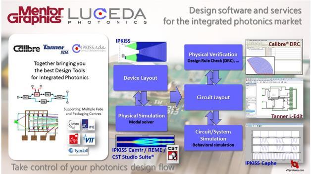
Design software and services for the integrated photonics market IPKISS Moves the edges in PIC PDK building
 Design software and services for the integrated photonics market IPKISS 3.1.3 Moves the edges in PIC PDK building take controltake of your control photonics of your photonics design flow design flow 1
Improved Circuit Reliability/Robustness. Carey Robertson Product Marketing Director Mentor Graphics Corporation
 Improved Circuit Reliability/Robustness Carey Robertson Product Marketing Director Mentor Graphics Corporation Reliability Requirements are Growing in all Market Segments Transportation Mobile / Wireless
AIM Photonics Silicon Photonics PDK Overview. March 22, 2017 Brett Attaway
 AIM Photonics Silicon Photonics PDK Overview March 22, 2017 Brett Attaway Silicon Photonics Process Design Kits (PDK) PDK 3 technologies, 2 major releases/year Full (active)- v1.0 available now Passive-
take control of your photonics design flow Photonic-Electronic IC design and implementation Pieter Dumon 27/09/2016
 take control of your photonics design flow Photonic-Electronic IC design and implementation Pieter Dumon 27/09/2016 Giving photonic IC designers the same power as electronic IC designers. Make it possible
Laker and Calibre RealTime, an OA Integration Success Story
 Silicon Integration Initiative Laker and Calibre RealTime, an OA Integration Success Story Rich Morse, Marketing & EDA Alliances Manager, SpringSoft Anant Adke, Director of Engineering, Design to Silicon
Computer-Based Project on VLSI Design Co 3/7
 Computer-Based Project on VLSI Design Co 3/7 IC Layout and Symbolic Representation This pamphlet introduces the topic of IC layout in integrated circuit design and discusses the role of Design Rules and
OpenDFM Targeting Functions. Bob Sayah June 6, 2011 IBM Corporation Si2 Targeting Working Group Chair
 OpenDFM Targeting Functions Bob Sayah June 6, 2011 IBM Corporation Si2 Targeting Working Group Chair Targeting Design Drawn Shapes Mfg. Targeting Targeting takes the Drawn Shapes provided by the layout
Physical Verification Challenges and Solution for 45nm and Beyond. Haifang Liao Celesda Design Solutions, Inc.
 Physical Verification Challenges and Solution for 45nm and Beyond Haifang Liao Celesda Design Solutions, Inc. Nanometer Design Era Semiconductor feature size has been shrunk 500x in 40 years Space for
Virtuoso Layout Suite XL
 Accelerated full custom IC layout Part of the Cadence Virtuoso Layout Suite family of products, is a connectivity- and constraint-driven layout environment built on common design intent. It supports custom
Achieve more with light.
 Achieve more with light. Comprehensive suite of leading photonic design tools. Component Design Multiphysics Component Design Lumerical s highly integrated suite of component design tools is purposebuilt
Concurrent, OA-based Mixed-signal Implementation
 Concurrent, OA-based Mixed-signal Implementation Mladen Nizic Eng. Director, Mixed-signal Solution 2011, Cadence Design Systems, Inc. All rights reserved worldwide. Mixed-Signal Design Challenges Traditional
Virtuoso Custom Design Platform GXL. Open Database. PDKs. Constraint Management. Customer IP
 Virtuoso Custom Design Platform GL The Cadence Virtuoso custom design platform is the industry s leading design system for complete front-to-back analog, RF, mixed-signal, and custom digital design. The
An overview of standard cell based digital VLSI design
 An overview of standard cell based digital VLSI design Implementation of the first generation AsAP processor Zhiyi Yu and Tinoosh Mohsenin VCL Laboratory UC Davis Outline Overview of standard cellbased
Design Solutions in Foundry Environment. by Michael Rubin Agilent Technologies
 Design Solutions in Foundry Environment by Michael Rubin Agilent Technologies Presenter: Michael Rubin RFIC Engineer, R&D, Agilent Technologies former EDA Engineering Manager Agilent assignee at Chartered
DATASHEET VIRTUOSO LAYOUT SUITE GXL
 DATASHEET Part of the Cadence Virtuoso Layout Suite family of products, is a collection of fully automated layout capabilities such as custom placement and routing, layout optimization, module generation,
Overview of Digital Design Methodologies
 Overview of Digital Design Methodologies ELEC 5402 Pavan Gunupudi Dept. of Electronics, Carleton University January 5, 2012 1 / 13 Introduction 2 / 13 Introduction Driving Areas: Smart phones, mobile devices,
OpenPDK Production Value and Benchmark Results
 OpenPDK Production Value and Benchmark Results Philippe MAGARSHACK Executive Vice-President, Design Enablement and Services June 2 nd, 2014 ST s Strong technology portfolio : Several R&D Partnerships &
Process Design Kit for for Flexible Hybrid Electronics (FHE-PDK)
") Process Design Kit for for Flexible Hybrid Electronics (FHE-PDK) Tsung-Ching Jim Huang, PhD Sr. Research Scientist, Hewlett Packard Labs MEPTEC2018 Outline Introduction Modeling and design needs for flexible
Process Design Kit for for Flexible Hybrid Electronics (FHE-PDK) Tsung-Ching Jim Huang, PhD Sr. Research Scientist, Hewlett Packard Labs MEPTEC2018 Outline Introduction Modeling and design needs for flexible
FinFET Technology Understanding and Productizing a New Transistor A joint whitepaper from TSMC and Synopsys
 White Paper FinFET Technology Understanding and Productizing a New Transistor A joint whitepaper from TSMC and Synopsys April, 2013 Authors Andy Biddle Galaxy Platform Marketing, Synopsys Inc. Jason S.T.
Taming the Challenges of Advanced-Node Design. Tom Beckley Sr. VP of R&D, Custom IC and Signoff, Silicon Realization Group ISQED 2012 March 20, 2012
 Taming the Challenges of Advanced-Node Design Tom Beckley Sr. VP of R&D, Custom IC and Signoff, Silicon Realization Group ISQED 2012 March 20, 2012 The custom design community Designers ( Relaxed attitude
DATASHEET VIRTUOSO LAYOUT SUITE FAMILY
 DATASHEET The Cadence Virtuoso Layout Suite family of products delivers a complete solution for front-to-back custom analog, digital, RF, and mixed-signal design. It preserves design intent throughout
Reduce Verification Complexity In Low/Multi-Power Designs. Matthew Hogan, Mentor Graphics
 Reduce Verification Complexity In Low/Multi-Power Designs. Matthew Hogan, Mentor Graphics BACKGROUND The increasing demand for highly reliable products covers many industries, all process nodes, and almost
PDK-Based Analog/Mixed-Signal/RF Design Flow 11/17/05
 PDK-Based Analog/Mixed-Signal/RF Design Flow 11/17/05 Silvaco s What is a PDK? Which people build, use, and support PDKs? How do analog/mixed-signal/rf engineers use a PDK to design ICs? What is an analog/mixed-signal/rf
Collaborate to Innovate FinFET Design Ecosystem Challenges and Solutions
 2013 TSMC, Ltd Collaborate to Innovate FinFET Design Ecosystem Challenges and Solutions 2 Agenda Lifestyle Trends Drive Product Requirements Concurrent Technology and Design Development FinFET Design Challenges
Taming the Challenges of 20nm Custom/Analog Design
 Taming the Challenges of 20nm Custom/Analog Design Custom and analog designers will lay the foundation for 20nm IC design. However, they face many challenges that arise from manufacturing complexity. The
MEMS Pro v5.1 Layout Tutorial Physical Design Mask complexity
 MEMS Pro v5.1 Layout Tutorial 1 Physical Design Mask complexity MEMS masks are complex with curvilinear geometries Verification of manufacturing design rules is important Automatic generation of mask layout
One-Shot DRC within a Fine-Grain Physical Verification Platform for advanced process nodes
 One-Shot DRC within a Fine-Grain Physical Verification Platform for advanced process nodes Last updated: May, 2017 To meet the challenge of nano-scale, deep sub-wavelength processes, innovative One -Shot
Will Silicon Proof Stay the Only Way to Verify Analog Circuits?
 Will Silicon Proof Stay the Only Way to Verify Analog Circuits? Pierre Dautriche Jean-Paul Morin Advanced CMOS and analog. Embedded analog Embedded RF 0.5 um 0.18um 65nm 28nm FDSOI 0.25um 0.13um 45nm 1997
3D Integration & Packaging Challenges with through-silicon-vias (TSV)
") NSF Workshop 2/02/2012 3D Integration & Packaging Challenges with through-silicon-vias (TSV) Dr John U. Knickerbocker IBM - T.J. Watson Research, New York, USA Substrate IBM Research Acknowledgements IBM
NSF Workshop 2/02/2012 3D Integration & Packaging Challenges with through-silicon-vias (TSV) Dr John U. Knickerbocker IBM - T.J. Watson Research, New York, USA Substrate IBM Research Acknowledgements IBM
Photonics Integration in Si P Platform May 27 th Fiber to the Chip
 Photonics Integration in Si P Platform May 27 th 2014 Fiber to the Chip Overview Introduction & Goal of Silicon Photonics Silicon Photonics Technology Wafer Level Optical Test Integration with Electronics
VLSI Lab Tutorial 3. Virtuoso Layout Editing Introduction
 VLSI Lab Tutorial 3 Virtuoso Layout Editing Introduction 1.0 Introduction The purpose of this lab tutorial is to guide you through the design process in creating a custom IC layout for your CMOS inverter
Silicon Photonics PDK Development
 Hewlett Packard Labs Silicon Photonics PDK Development M. Ashkan Seyedi Large-Scale Integrated Photonics Hewlett Packard Labs, Palo Alto, CA ashkan.seyedi@hpe.com Outline Motivation of Silicon Photonics
Advanced multi-patterning and hybrid lithography techniques. Fedor G Pikus, J. Andres Torres
 Advanced multi-patterning and hybrid lithography techniques Fedor G Pikus, J. Andres Torres Outline Need for advanced patterning technologies Multipatterning (MP) technologies What is multipatterning?
An Automated System for Checking Lithography Friendliness of Standard Cells
 An Automated System for Checking Lithography Friendliness of Standard Cells I-Lun Tseng, Senior Member, IEEE, Yongfu Li, Senior Member, IEEE, Valerio Perez, Vikas Tripathi, Zhao Chuan Lee, and Jonathan
Expert Layout Editor. Technical Description
 Expert Layout Editor Technical Description Agenda Expert Layout Editor Overview General Layout Editing Features Technology File Setup Multi-user Project Library Setup Advanced Programmable Features Schematic
LiTE Design PORTFOLIO
 LiTE Design We Focus on scaling to new & latest technology in Electronic Design System, to develop & produce innovative products, services & solutions with our Potential that Exceeds the expectations of
Comprehensive Place-and-Route Platform Olympus-SoC
 Comprehensive Place-and-Route Platform Olympus-SoC Digital IC Design D A T A S H E E T BENEFITS: Olympus-SoC is a comprehensive netlist-to-gdsii physical design implementation platform. Solving Advanced
AN INTRODUCTION TO HYPERLYNX SI/PI TECHNOLOGY
 AN INTRODUCTION TO HYPERLYNX SI/PI TECHNOLOGY BY STEVE KAUFER, MENTOR H I G H S P E E D D E S I G N W H I T E P A P E R OVERVIEW Digital designers are now required to make the leap from time domain to
Lab. Course Goals. Topics. What is VLSI design? What is an integrated circuit? VLSI Design Cycle. VLSI Design Automation
 Course Goals Lab Understand key components in VLSI designs Become familiar with design tools (Cadence) Understand design flows Understand behavioral, structural, and physical specifications Be able to
Xilinx SSI Technology Concept to Silicon Development Overview
 Xilinx SSI Technology Concept to Silicon Development Overview Shankar Lakka Aug 27 th, 2012 Agenda Economic Drivers and Technical Challenges Xilinx SSI Technology, Power, Performance SSI Development Overview
Laker 3 Custom Design Tools
 Datasheet Laker 3 Custom Design Tools Laker 3 Custom Design Tools The Laker 3 Custom Design Tools form a unified front-to-back environment for custom circuit design and layout. They deliver a complete
idrm: Fixing the broken interface between design and manufacturing
 idrm: Fixing the broken interface between design and manufacturing Abstract Sage Design Automation, Inc. Santa Clara, California, USA This paper reviews the industry practice of using the design rule manual
CMP Model Application in RC and Timing Extraction Flow
 INVENTIVE CMP Model Application in RC and Timing Extraction Flow Hongmei Liao*, Li Song +, Nickhil Jakadtar +, Taber Smith + * Qualcomm Inc. San Diego, CA 92121 + Cadence Design Systems, Inc. San Jose,
TABLE OF CONTENTS 1.0 PURPOSE INTRODUCTION ESD CHECKS THROUGHOUT IC DESIGN FLOW... 2
 TABLE OF CONTENTS 1.0 PURPOSE... 1 2.0 INTRODUCTION... 1 3.0 ESD CHECKS THROUGHOUT IC DESIGN FLOW... 2 3.1 PRODUCT DEFINITION PHASE... 3 3.2 CHIP ARCHITECTURE PHASE... 4 3.3 MODULE AND FULL IC DESIGN PHASE...
Evolution of CAD Tools & Verilog HDL Definition
 Evolution of CAD Tools & Verilog HDL Definition K.Sivasankaran Assistant Professor (Senior) VLSI Division School of Electronics Engineering VIT University Outline Evolution of CAD Different CAD Tools for
Guardian NET Layout Netlist Extractor
 Outline What is Guardian NET Key Features Running Extraction Setup Panel Layout Annotation Layout Text Extraction Node Naming Electric Rule Checking (ERC) Layout Hierarchy Definition Hierarchy Checker
PACKAGE DESIGNERS NEED ASSEMBLY-LEVEL LVS FOR HDAP VERIFICATION TAREK RAMADAN MENTOR, A SIEMENS BUSINESS
 PACKAGE DESIGNERS NEED ASSEMBLY-LEVEL LVS FOR HDAP VERIFICATION TAREK RAMADAN MENTOR, A SIEMENS BUSINESS D E S I G N T O S I L I C O N W H I T E P A P E R w w w. m e n t o r. c o m INTRODUCTION Contrary
CHAPTER 3 SIMULATION TOOLS AND
 CHAPTER 3 SIMULATION TOOLS AND Simulation tools used in this simulation project come mainly from Integrated Systems Engineering (ISE) and SYNOPSYS and are employed in different areas of study in the simulation
An Overview of Standard Cell Based Digital VLSI Design
 An Overview of Standard Cell Based Digital VLSI Design With examples taken from the implementation of the 36-core AsAP1 chip and the 1000-core KiloCore chip Zhiyi Yu, Tinoosh Mohsenin, Aaron Stillmaker,
RSoft Product Applications
 RSoft Product Applications Complete design solutions for photonic components, circuits and systems synopsys.com/optical-solutions/rsoft RSoft Photonic Design Software Applications Synopsys RSoft products
Open Process Spec Adoption: a Case Study
 Open Process Spec Adoption: a Case Study June 3 rd, 2014 AGENDA 2 OpenPDK & OPS Introduction What does OPS looks like? Let s do an openpdk with OPS Target of OpenPDK Coalition 3 a set of open standards
A Novel Methodology for Triple/Multiple-Patterning Layout Decomposition
 A Novel Methodology for Triple/Multiple-Patterning Layout Decomposition Rani S. Ghaida 1, Kanak B. Agarwal 2, Lars W. Liebmann 3, Sani R. Nassif 2, Puneet Gupta 1 1 UCLA, Electrical Engineering Dept. 2
VLSI Design Automation
 VLSI Design Automation IC Products Processors CPU, DSP, Controllers Memory chips RAM, ROM, EEPROM Analog Mobile communication, audio/video processing Programmable PLA, FPGA Embedded systems Used in cars,
A Method to Implement Layout Versus Schematic Check in Integrated Circuits Design Programs
 A Method to Implement Layout Versus Schematic Check in Integrated Circuits Design Programs Radu Gabriel Bozomitu, Daniela Ionescu Telecommunications Department Faculty of Electronics and Telecommunications,
Power dissipation! The VLSI Interconnect Challenge. Interconnect is the crux of the problem. Interconnect is the crux of the problem.
 The VLSI Interconnect Challenge Avinoam Kolodny Electrical Engineering Department Technion Israel Institute of Technology VLSI Challenges System complexity Performance Tolerance to digital noise and faults
OpenAccess PCells Ed Petrus VP Engineering V2
 OpenAccess PCells Ed Petrus VP Engineering V2 April 2005 Page 1 Copyright 2005 CiraNova, Inc. What is CiraNova about? 4 CiraNova enables analog designers to create migratable, re-usable analog objects
Baseband IC Design Kits for Rapid System Realization
 Baseband IC Design Kits for Rapid System Realization Lanbing Chen Cadence Design Systems Engineering Director John Rowland Spreadtrum Communications SVP of Hardware Engineering Agenda How to Speed Up IC
Taurus-Device. Multidimensional Device Simulation SYSTEMS PRODUCTS LOGICAL PRODUCTS PHYSICAL IMPLEMENTATION SIMULATION AND ANALYSIS LIBRARIES TCAD
 SYSTEMS PRODUCTS LOGICAL PRODUCTS PHYSICAL IMPLEMENTATION SIMULATION AND ANALYSIS LIBRARIES TCAD Aurora DFM WorkBench Davinci Medici Raphael Raphael-NES Silicon Early Access TSUPREM-4 Taurus-Device Taurus-Lithography
EEM870 Embedded System and Experiment Lecture 2: Introduction to SoC Design
 EEM870 Embedded System and Experiment Lecture 2: Introduction to SoC Design Wen-Yen Lin, Ph.D. Department of Electrical Engineering Chang Gung University Email: wylin@mail.cgu.edu.tw March 2013 Agenda
Topology Router. - The Intelligence of an Engineer. - The Skill of a Designer - The Speed of Auto-Routing. Dave Wiens. Director, Market Development
 Topology Router - The Intelligence of an Engineer - The Skill of a Designer - The Speed of Auto-Routing Dave Wiens Director, Market Development Challenges Reduction of design-cycle time for products that
NetSpeed ORION: A New Approach to Design On-chip Interconnects. August 26 th, 2013
 NetSpeed ORION: A New Approach to Design On-chip Interconnects August 26 th, 2013 INTERCONNECTS BECOMING INCREASINGLY IMPORTANT Growing number of IP cores Average SoCs today have 100+ IPs Mixing and matching
Cadence Virtuoso Schematic Design and Circuit Simulation Tutorial
 Cadence Virtuoso Schematic Design and Circuit Simulation Tutorial Introduction This tutorial is an introduction to schematic capture and circuit simulation for ENGN1600 using Cadence Virtuoso. These courses
Detailed Presentation
 Detailed Presentation PDK Leadership - Developing and Delivering High Quality PDKs Simucad PDKs are being rapidly adopted worldwide by leading foundries and design houses because of their quality and ease
ECE520 VLSI Design. Lecture 1: Introduction to VLSI Technology. Payman Zarkesh-Ha
 ECE520 VLSI Design Lecture 1: Introduction to VLSI Technology Payman Zarkesh-Ha Office: ECE Bldg. 230B Office hours: Wednesday 2:00-3:00PM or by appointment E-mail: pzarkesh@unm.edu Slide: 1 Course Objectives
In-design DFM rule scoring and fixing method using ICV
 In-design DFM rule scoring and fixing method using ICV Vikas Tripathi, Yongfu Li, Zhao Chuan Lee, I-Lun Tseng, Jason Khaw and Jonathan Ong Globalfoundries Singapore Pte. Ltd. Singapore www.globalfoundries.com
Design of a Low Density Parity Check Iterative Decoder
 1 Design of a Low Density Parity Check Iterative Decoder Jean Nguyen, Computer Engineer, University of Wisconsin Madison Dr. Borivoje Nikolic, Faculty Advisor, Electrical Engineer, University of California,
ASIC design flow considering lithography-induced effects
 DESIGN FOR MANUFACTURABILITY ASIC design flow considering lithography-induced effects K. Cao and J. Hu Abstract: As VLSI technology scales towards 65 nm and beyond, both timing and power performance of
VLSI Design Automation
 VLSI Design Automation IC Products Processors CPU, DSP, Controllers Memory chips RAM, ROM, EEPROM Analog Mobile communication, audio/video processing Programmable PLA, FPGA Embedded systems Used in cars,
Visual Design Flows for Faster Debug and Time to Market FlowTracer White Paper
 Visual Design Flows for Faster Debug and Time to Market FlowTracer White Paper 2560 Mission College Blvd., Suite 130 Santa Clara, CA 95054 (408) 492-0940 Introduction As System-on-Chip (SoC) designs have
Improve Reliability With Accurate Voltage-Aware DRC. Matthew Hogan, Mentor Graphics
 Improve Reliability With Accurate Voltage-Aware DRC Matthew Hogan, Mentor Graphics BACKGROUND Consumer expectations for longer device operations at sustained performance levels means designing for reliability
On the Complexity of Graph Cuboidal Dual Problems for 3-D Floorplanning of Integrated Circuit Design
 On the Complexity of Graph Cuboidal Dual Problems for 3-D Floorplanning of Integrated Circuit Design Renshen Wang Chung-Kuan Cheng Department of Computer Science & Engineering University of California,
Galaxy Custom Designer LE Custom Layout Editing
 Datasheet Galaxy Custom Designer LE Custom Layout Editing Overview Galaxy Custom Designer LE is the modern-era choice for layout entry and editing, enabling users to meet the challenges of today s fast-moving
Laker Custom Layout Automation System
 The Laker Custom Layout offers powerful solutions for analog, mixed-signal, memory, and custom digital IC design that address key pain points in the layout process. The Laker layout system provides an
Mm-wave integrated waveguide components in silicon technology
 Mm-wave integrated waveguide components in silicon technology G. Gentile, M. Spirito, L.C.N. de Vreede, et al. Electronics Research Laboratory (ELCA), Dimes, Delft University of Technology, The Netherlands
Introduction to AWR Design Flow and New Features for V10
 Introduction to AWR Design Flow and New Features for V10 What s New In Version 10 imatch Matching Network Synthesis Matching Network Synthesis Tight integration with AWR tools Excellent starting point
Lab 9 PCB Design & Layout
 Lab 9 PCB Design & Layout ECT 224L Department of Engineering Technology Lab 9 PCB Traces Size dependent upon electrical requirements, design constraints (routing space and clearance), and trace/space resolution
Joe Civello ADS Product Manager/ Keysight EEsof EDA
 Joe Civello 2018.01.11 ADS Product Manager/ Keysight EEsof EDA 3D Layout Viewing directly from the Layout Window 3D Editing & Routing PCB & IC/Module Design Dramatically Improved Visual Inspection Simplified
Emerging Platforms, Emerging Technologies, and the Need for Crosscutting Tools Luca Carloni
 Emerging Platforms, Emerging Technologies, and the Need for Crosscutting Tools Luca Carloni Department of Computer Science Columbia University in the City of New York NSF Workshop on Emerging Technologies
Full Custom Layout Optimization Using Minimum distance rule, Jogs and Depletion sharing
 Full Custom Layout Optimization Using Minimum distance rule, Jogs and Depletion sharing Umadevi.S #1, Vigneswaran.T #2 # Assistant Professor [Sr], School of Electronics Engineering, VIT University, Vandalur-
EDA for ONoCs: Achievements, Challenges, and Opportunities. Ulf Schlichtmann Dresden, March 23, 2018
 EDA for ONoCs: Achievements, Challenges, and Opportunities Ulf Schlichtmann Dresden, March 23, 2018 1 Outline Placement PROTON (nonlinear) PLATON (force-directed) Maze Routing PlanarONoC Challenges Opportunities
Fabrication of partially double-curved surfaces out of flat sheet material through a 3d puzzle approach
 Fabrication of partially double-curved surfaces out of flat sheet material through a 3d puzzle approach tn03-081 Abstract The topic of this paper is connection of digital modeling with generative programming
Manufacturing Challenges and their Implications on Design
 Manufacturing Challenges and their Implications on Design Phiroze Parakh, Ph.D 45nm/32nm Design Challenges MANUFACTURING VARIATIONS PROCESS & DESIGN VARIATIONS LARGE DESIGNS LOW POWER The Evolution of
DEVELOPMENT OF PARAMETERIZED CELL OF SPIRAL INDUCTOR USING SKILL LANGUAGE
 DEVELOPMENT OF PARAMETERIZED CELL OF SPIRAL INDUCTOR USING SKILL LANGUAGE Vladimir Emilov Grozdanov 1, Diana Ivanova Pukneva 1, Marin Hristov Hristov 2 1 Smartcom, 7 th km, Tzarigradsko Chausee Blvd, 1784
HIGH SPEED TDI EMBEDDED CCD IN CMOS SENSOR
 HIGH SPEED TDI EMBEDDED CCD IN CMOS SENSOR P. Boulenc 1, J. Robbelein 1, L. Wu 1, L. Haspeslagh 1, P. De Moor 1, J. Borremans 1, M. Rosmeulen 1 1 IMEC, Kapeldreef 75, B-3001 Leuven, Belgium Email: pierre.boulenc@imec.be,
On-Chip Communications
 On-Chip Communications Somayyeh Koohi Department of Computer Engineering Sharif University of Technology 1 Introduction Adapted with modifications from lecture notes prepared by S.Pasricha and N.Dutt Outline
Allegro Sigrity SI Streamlining the creation of high-speed interconnect on digital PCBs and IC packages
 Streamlining the creation of high-speed interconnect on digital PCBs and IC packages The Cadence Allegro Sigrity signal integrity (SI) integrated high-speed design and analysis environment streamlines
Pushing 193i lithography by Joint optimization of Layout and Lithography
 Pushing 193i lithography by Joint optimization of Layout and Lithography Peter De Bisschop Imec, Leuven, Belgium Semicon Europe Messe Dresden, Germany Lithography session October 12, 2011 Semiconductor-Industry
Recognizing Deformable Shapes. Salvador Ruiz Correa Ph.D. UW EE
 Recognizing Deformable Shapes Salvador Ruiz Correa Ph.D. UW EE Input 3-D Object Goal We are interested in developing algorithms for recognizing and classifying deformable object shapes from range data.
FABRICATION OF CMOS INTEGRATED CIRCUITS. Dr. Mohammed M. Farag
 FABRICATION OF CMOS INTEGRATED CIRCUITS Dr. Mohammed M. Farag Outline Overview of CMOS Fabrication Processes The CMOS Fabrication Process Flow Design Rules EE 432 VLSI Modeling and Design 2 CMOS Fabrication
PDK Automation An IBM Perspective
 PDK utomation n IBM Perspective Matthew Graf, OPDKC James Culp, ODFMC Si2 Con Oct. 20 th, 2011 IBM s PDK Development History Timeline 1998 2009 OpenPDK OpenDFM Chip Design groups develop their own PDK
SRAM Memory Layout Design in 180nm Technology
 SRAM Memory Layout Design in 180nm Technology Praveen K N M.Tech in VLSI Design & Embedded Systems JSS Academy of Technical Education, Bengaluru, India B. G. Shivaleelavathi Professor, H.O. D ECE Department,
Driving Semiconductor Industry Optimization From. Walden C. Rhines. CHAIRMAN & CEO Mentor Graphics Corporation
 Driving Semiconductor Industry Optimization From U.S.-Taiwan-China Relationships Walden C. Rhines CHAIRMAN & CEO Mentor Graphics Corporation U.S.-Taiwan-China Semiconductor Optimization Growing the total
UNIVERSITY OF WATERLOO
 UNIVERSITY OF WATERLOO UW ASIC DESIGN TEAM: Cadence Tutorial Description: Part I: Layout & DRC of a CMOS inverter. Part II: Extraction & LVS of a CMOS inverter. Part III: Post-Layout Simulation. The Cadence
Keysight Technologies Integrating Multiple Technology Devices onto Laminate-Based Multi-Chip-Modules Using an Integrated Design Flow
 Keysight Technologies Integrating Multiple Technology Devices onto Laminate-Based Multi-Chip-Modules Using an Integrated Design Flow Article Reprint This article was first published in Microwave Product
Reducing shot count through Optimization based fracture
 Reducing shot count through Optimization based fracture Timothy Lin a, Emile Sahouria a, Nataraj Akkiraju a, Steffen Schulze b a Mentor Graphics Corporation, 46871 Bayside Parkway, Fremont, CA 94538 b
Latch-up Verification / Rule Checking Throughout Circuit Design Flow
 Latch-up Verification / Rule Checking Throughout Circuit Design Flow Michael Khazhinsky ESD and Latch-up Design Silicon Labs April 2016 Motivation The verification of latch-up protection networks in modern