Anatomy of a Post PC Device. Prof. S.E Thompson EEE4310/5322 Fall 2017
|
|
|
- Janel Wiggins
- 5 years ago
- Views:
Transcription

1 Anatomy of a Post PC Device iphone 7 Samsung Galaxy S8 Prof. S.E Thompson EEE4310/5322 Fall 2017

2 Modern Computer or Mobile Computer? Samsung Galaxy S8 2 More than mobile computer - Robotics - Drones - Future laptops?

3 Logic, DRAM, NAND, Power Management, Analog/RF Iphone 7 X NAND Flash memory 3 Printed Circuit Boards: mechanically supports and electrically connects electronic components - etched copper sheets laminated onto non-conductive substrate - FR-4 glass epoxy (fibre Reinforced plastic)
4 Cost Per Bit of Storage in Mobile Computer: SRAM, DRAM, NAND Memory Memory Unit Cell Area SRAM 6 Transistors ~(60 80) f 2 DRAM 1 Transistor 1 Capacitor ~6 f 2 NAND 1 Transistor ~2 f 2 Why is 3 different types of memory needed in a computer? f = feature size Cost ~ area but only if processed wafer cost the same Other attributes: read/write speed/power, endurance, dynamic vs static, volatile vs nonvolitle 4


5 System On A Chip (SOC) Chip becomes a system Chip includes processors, memory, ASIC, Analog I/O + more Software Complexity Test Why did SOC start in mobile computing? space and cost 5 Source: Dimas Ruliandi: System on Chip Design, Architecture and Applications

6 System On A Chip: SOC: Space and Cost Vs SoC vs. CPU The battle for the future of computing DDR3/PCI Express signals vs on SOC 6
7 History of Computing 7 Source: Pushkar Ranade and Scott Thompson, SuVolta Inc.


8 iphone: SOC / Baseband On Same PCB Iphone 5S Logic Board Source: ifixit 8

9 Samsung S8 Chips/Cost Memory - Leading edge feature size 9 Application processor/modems - Leading edge feature size - often on same chip

10 iphone 1: 2007 Leading Edge ~ 90nm Camera: 2.0 MP with geotagging Processor: Apple-branded 412 MHz 32-bit Samsung ARM 11 with PowerVR MBX-Lite GPU Specified by Apple and manufactured by Samsung Single ARM CPU Samsung 90nm RAM: 128 MB edram Sold 6.1million units Storage 4, 8 or 16GB G about 1 billion 8bits in 1 Byte ~ 2bits per 1 transistor Data input: Multi-touch touchscreen 10 Homework: read by next class Intel s From Sand to Circuits in week 1 e-learning

11 90nm Silicon Gate Transistor (TSMC) TEM image Silicon gate technology Poly-Silicon Self-aligned Source/drain + Speed + Reliability + Density Key metrics Contact to gate pitch Transistor size ~90nm Silicide Metal on source/drain/gate W contacts Cu wires 11 Source: chipworks
12 History: Bell Labs First Insulated Gate Field Effect Transistor (FET) First Transistor 1947 (Shockley/Bardeen/Brattain) FET Demonstrated in 1959 But anticipated in Lilienfeld s 1926 patent Fabrication challenge Surface state challenge Thermally grown SiO2 provided good interface Why Si vs Ge or GaN or GaAs? 12
13 History: Complementary MOS (CMOS Invented 1963) N and P type transistors Allows low leakage circuits Required for VLSI N and P transistor network between supply and ground. One type always off 13


14 History: Invention of Integrated Circuit ~1959 There is no consensus on who invented the IC. The American press of the 1960s named four people: Kilby, Lehovec, Noyce and Hoerni Electronic circuits on single device patents in 1950 s 1970s the list was shortened to Kilby and Noyce, and then to Kilby, who was awarded the 2000 Nobel Prize in Physics "for his part in the invention of the integrated circuit ss Noyce: 1959 planar integrated circuit 14 Source: wikipedi Logical NOR IC from Apollo spacecraft

15 15 Read Intel s Tutorial
 Fundamental")

16 Pattern Transfer to Wafer Allows local Etch Ion implant (electrical properties n or p Silicon) Fundamental processes to build microstructures Lithography Etch, Ion implant Diffusion Deposition Polish Theramal annealing Source: Intel 16


17 Post Chip Fabrication Wafer/Sort test Yield Functionality Wafer dicing Packaging 17


18 A7 (28nm) in iphone 5s (2013) Intel 32nm chip 18 PC class like computer? First 64bit chip to ship in a smartphone Over 1 Billion transistors Manufactured Samsung Ghz Why not wide range of CPU clock freq. like Intel CPU


19 Strained Si / Metal Gate 19 Conventional scaling of poly-si gate transistor prior to 90nm Dennard scaling theory (0.7X) 2X transistor density New manufacturing node every 2 or 3 years
 http://www.dailytech.com/die+shots+confirm+a8+packs+six+powerv R+Rogue+GPU+Clusters/article36586.")
20 A8 ( 20nm) in iphone 6 (2014) 20nm process TSMC and Samsung Twice the number of transistors of the A7 13% smaller physical chip size (89mm 2 ) R+Rogue+GPU+Clusters/article36586.htm 20
 Fabricated in")


21 A9 (16nm) in iphone 6S (2015) Fabricated in 16nm FinFET / TSMC Fabricated 14nm FinFET / Samsung Samsung A Ghz A64 GPU (six Cores)

22 Introduction to FinFET Source Intel FinFET width =? 22
")


23 A10 (16nm) in iphone 7 (2016) A10 die size is ~125 sq. mm 3.3 billion transistors. TSMC 16FF-based 23
24 24

25 A11 in iphone 8 (2017) 10nm TSMC Estimate 100 million chips will be manufactured in 2017 Number of transistor? > 3 B 25


26 First 10nm in Samsung S8 Snapdragon 835 > 3B transistors In area < penny CPU/GPU/LTE/WiFi and more What does 10nm mean? 26

27 Top Down Circuit View of CMOS TSMC 28nm CMOS logic style N and P logic stacks 27
28 28 Type of Chips / Summary Chip Technology Some Metric SOC Baseband NAND Flash DRAM Image sensor NFC / Microcontrollers/ RF chips Power Amplifiers Motion sensors Power Switches Filters Leading edge logic - Minimum low V transistors / CMOS - Few 2.5/3.3 Analog I/O Metal Layers Leading edge memory - mimimum feature floating gate 1T Leading edge memory - minimum feature 1T1C ~65nm photo diode, plus capacitor and transistors ~65 to 130nm - Analog, RF, envm ~ >100 nm GaAs, GaN, SOI phemt or HBT ~ > 100nm Sensor category: Capacitive, Piezoelectric, Piezoresistive ~ >100nm GaAs, GaN, SOI PHEMT or HBT ~> 100nm Surface acoustic wave (SAW) filters Interleaved metal / piezoelectric substrate PMIC 65 to 180nm - BiCMOS Process technology High Voltage (5.0, 3.3, 2.5, 1.8V) Transistors, Analog Cost /transistor Digital logic Power Cost per NVM bit Cost per RAM bit Picture quality Cost Power (uw) Power added efficiency (PAE) Sense Acceleration or Rotation Loss Low insertion loss with good rejection High efficiency power conversions


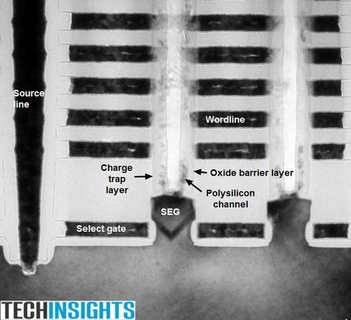
29 NAND Memory in iphone 7 A true 3D chip 48 device layers 29
 https://en.m.wikipedia.")
30 NAND FLASH Chip Basics Single NAND Flash transistor String of transistors (NAND circuit) 30

31 Program/Erase NAND Flash ~20V Source: How is 20V supplied inside a cell phone? 31
 node.")

32 TEM NAND Flash: Samsung 90nm State of art planar NAND memory is 1x (nm) node. 2-3 bits per cell MLC) 32
33 Program and Inhibit SGD V high = 10V V high = 10V V high = 10V V high = 10V V PGM = 20V V high = 10V V high = 10V V high = 10V V high = 10V BL 0 BL 1 BL 2 BL 3 BL 4 8V 8V 8V 0V 8V WL0 WL1 WL2 WL3 WL4 WL5 WL6 WL7 WL8 SGC Well = 0V Inhibit 20V 20V Program 33 8V 8V 0V 0V 0V
34 Read Number of Cells SGD V high = 7V V high = 7V BL 0 BL 1 BL 2 BL 3 BL 4 0V 0V 0V 1V 0V WL0 WL1 Erased Cells V high = 7V V high = 7V Programed Cells V READ = RAMP V high = 7V V high = 7V WL2 WL3 WL4 WL5 WL6 Threshold Voltage Logic 1 Logic 0 V high = 7V V high = 7V SGC WL7 WL8 Well = 0V I READ RAMP V 34
35 ERASE Erased Cells Number of Cells Threshold Voltage Programed Cells Logic 1 Logic 0 SGD V high = 0V V high = 0V V high = 0V V high = 0V V high = 0V V high = 0V V high = 0V V high = 0V V high = 0V SGC BL 0 BL 1 BL 2 BL 3 BL 4 Float Float Float Float Float WL0 WL1 WL2 WL3 WL4 WL5 WL6 WL7 WL8 Well = 20V 0 V 35 20V
36 Block and Page BL 0 BL 1 BL 2 BL 3 BL 4 SGD WL0 Block WL1 Block size Some chips can set block to be SLC or MLC WL2 WL3 WL4 WL5 WL6 Page WL7 WL8 SGC 36 Page Buffer


37 Page / Block / Chip /Multi Chip in Package


38 3D NAND Memory NAND in iphone 7 Source: Andy Walker 38


39 39 2TB Solid State Drive How Many Transistors in Small Space?
40 40 Type of Chips / Summary Chip Technology Some Metric SOC Baseband NAND Flash DRAM Image sensor NFC / Microcontrollers/ RF chips Power Amplifiers Motion sensors Power Switches Filters Leading edge logic - Minimum low V transistors / CMOS - Few 2.5/3.3 Analog I/O Metal Layers Leading edge memory - mimimum feature floating gate 1T Leading edge memory - minimum feature 1T1C ~65nm photo diode, plus capacitor and transistors ~65 to 130nm - Analog, RF, envm ~ >100 nm GaAs, GaN, SOI phemt or HBT ~ > 100nm Sensor category: Capacitive, Piezoelectric, Piezoresistive ~ >100nm GaAs, GaN, SOI PHEMT or HBT ~> 100nm Surface acoustic wave (SAW) filters Interleaved metal / piezoelectric substrate PMIC 65 to 180nm - BiCMOS Process technology High Voltage (5.0, 3.3, 2.5, 1.8V) Transistors, Analog Cost /transistor Digital logic Power Cost per NVM bit Cost per RAM bit Picture quality Cost Power (uw) Power added efficiency (PAE) Sense Acceleration or Rotation Loss Low insertion loss with good rejection High efficiency power conversions


41 DRAM in Mobile Computer Iphone 5s Package on package PC uses DIMM 41

42 DRAM (Simple) V CC /2 42
43 Simple DRAM CELL VCC/2 43

44 DRAM (simple) Embedded DRAM in Microsoft Xbox GPU fabbed by TSMC (65-nm) 44 m/2014/02/intels-e-dram-shows-upin-wild.html
 node in 2017 45 Source:")

45 State Of The Art DRAM Cylinder cell since ~2005 Slowing of DRAM density 1x (nm) node in Source:
46 46 Type of Chips / Summary Chip Technology Some Metric SOC Baseband NAND Flash DRAM Image sensor NFC / Microcontrollers/ RF chips Power Amplifiers Motion sensors Power Switches Filters Leading edge logic - Minimum low V transistors / CMOS - Few 2.5/3.3 Analog I/O Metal Layers Leading edge memory - mimimum feature floating gate 1T Leading edge memory - minimum feature 1T1C ~40-65nm photo diode, plus capacitor and transistors ~65 to 130nm - Analog, RF, envm ~ >100 nm GaAs, GaN, SOI phemt or HBT ~ > 100nm Sensor category: Capacitive, Piezoelectric, Piezoresistive ~ >100nm GaAs, GaN, SOI PHEMT or HBT ~> 100nm Surface acoustic wave (SAW) filters Interleaved metal / piezoelectric substrate PMIC 65 to 180nm - BiCMOS Process technology High Voltage (5.0, 3.3, 2.5, 1.8V) Transistors, Analog Cost /transistor Digital logic Power Cost per NVM bit Cost per RAM bit Picture quality Cost Power (uw) Power added efficiency (PAE) Sense Acceleration or Rotation Loss Low insertion loss with good rejection High efficiency power conversions

47 47 iphone 6 Board (Camera)

48 48 CMOS Camera


49 Stacked Image Sensor Module Power Problem Image Sensor Analog Pixels Image Digital Co-Processor Lower power Lower heat dissipation Package Lower thermal envelope Thinner package Sony 8Mpixal in Iphone 5S Stacked die TSV Through silicon vias
 is an image sensor consisting of an integrated circuit containing an array of pixel sensors, each pixel containing a photodetector and an active")
50 Simple CMOS Image Pixel Reverse biased Photo diode Source: Chipworks BSI Back Side Image of Light use in high end phones (iphone, Galaxy, etc) An active-pixel sensor (APS) is an image sensor consisting of an integrated circuit containing an array of pixel sensors, each pixel containing a photodetector and an active amplifier.

51 How CMOS Does Colors

 Initially")

52 M7: Always On Logic Chip Logic chip but fabricated with slow but ultra low leakage transitor (very high threshold voltage) Initially old process node (>90nm) but now can be on SOC with specialty transistor 52

53 RFID Passive and active RFID tag Magnetic field also provides power. Store tag info in embedded NVM 53 Source:
 Named BCD http://cellphonerepairtutorials.blogspot.")
54 Power Management IC Lithium cell voltage 3.7 ~3 V Manage, control and distribute and supply power voltages from the battery source to other corresponding circuits or chips. Convert, regulate, stabilize current and voltages Fabricated in older logic nodes with lots of added devices BJT, CMOS, DMOS (Double Diffused) Named BCD 54


55 Power Amplifiers Source: Chipworks Skyworks 5 Ghz power amp die Metrics: efficiency and linearity Best in high mobility semiconductors with large bandgap Fabricated at large feature size On chip high Q inductors Few different technology options: III-V-compound-based technologies (GaN, GaAs, SiC) and silicon-based (CMOS, BJT and SiGe-HBT) Si based technology has advantage for cost and integration with RF front-end Enhancement-mode MOSFETs and BJT 55 Source:
56 56 Future Trends?
Moore s Law: Alive and Well. Mark Bohr Intel Senior Fellow
 Moore s Law: Alive and Well Mark Bohr Intel Senior Fellow Intel Scaling Trend 10 10000 1 1000 Micron 0.1 100 nm 0.01 22 nm 14 nm 10 nm 10 0.001 1 1970 1980 1990 2000 2010 2020 2030 Intel Scaling Trend
The Memory Hierarchy 1
 The Memory Hierarchy 1 What is a cache? 2 What problem do caches solve? 3 Memory CPU Abstraction: Big array of bytes Memory memory 4 Performance vs 1980 Processor vs Memory Performance Memory is very slow
Advanced Information Storage 11
 Advanced Information Storage 11 Atsufumi Hirohata Department of Electronics 16:00 11/November/2013 Monday (P/L 002) Quick Review over the Last Lecture Shingled write recording : * Bit patterned media (BPM)
Introduction to ICs and Transistor Fundamentals
 Introduction to ICs and Transistor Fundamentals A Brief History 1958: First integrated circuit Flip-flop using two transistors Built by Jack Kilby at Texas Instruments 2003 Intel Pentium 4 mprocessor (55
iphone 5 and iphone 7 (April 14 and 17, 2017) iphone 5 WiFi module iphone 7 battery application processors wafer level packaging 3D NAND
 iphone 5 WiFi module iphone 7 battery application processors wafer level packaging 3D NAND") iphone 5 and iphone 7 (April 14 and 17, 2017) iphone 5 WiFi module iphone 7 battery application processors wafer level packaging 3D NAND 1 iphone 5 2 WiFi Front End in iphone 5 3 Broadcom BCM4334 inside
iphone 5 and iphone 7 (April 14 and 17, 2017) iphone 5 WiFi module iphone 7 battery application processors wafer level packaging 3D NAND 1 iphone 5 2 WiFi Front End in iphone 5 3 Broadcom BCM4334 inside
Advanced Heterogeneous Solutions for System Integration
 Advanced Heterogeneous Solutions for System Integration Kees Joosse Director Sales, Israel TSMC High-Growth Applications Drive Product and Technology Smartphone Cloud Data Center IoT CAGR 12 17 20% 24%
EECS 598: Integrating Emerging Technologies with Computer Architecture. Lecture 10: Three-Dimensional (3D) Integration
 Integration") 1 EECS 598: Integrating Emerging Technologies with Computer Architecture Lecture 10: Three-Dimensional (3D) Integration Instructor: Ron Dreslinski Winter 2016 University of Michigan 1 1 1 Announcements
1 EECS 598: Integrating Emerging Technologies with Computer Architecture Lecture 10: Three-Dimensional (3D) Integration Instructor: Ron Dreslinski Winter 2016 University of Michigan 1 1 1 Announcements
CMPEN 411 VLSI Digital Circuits. Lecture 01: Introduction
 CMPEN 411 VLSI Digital Circuits Kyusun Choi Lecture 01: Introduction CMPEN 411 Course Website link at: http://www.cse.psu.edu/~kyusun/teach/teach.html [Adapted from Rabaey s Digital Integrated Circuits,
NAND Flash Memory: Basics, Key Scaling Challenges and Future Outlook. Pranav Kalavade Intel Corporation
 NAND Flash Memory: Basics, Key Scaling Challenges and Future Outlook Pranav Kalavade Intel Corporation pranav.kalavade@intel.com October 2012 Outline Flash Memory Product Trends Flash Memory Device Primer
Introduction 1. GENERAL TRENDS. 1. The technology scale down DEEP SUBMICRON CMOS DESIGN
 1 Introduction The evolution of integrated circuit (IC) fabrication techniques is a unique fact in the history of modern industry. The improvements in terms of speed, density and cost have kept constant
More Course Information
 More Course Information Labs and lectures are both important Labs: cover more on hands-on design/tool/flow issues Lectures: important in terms of basic concepts and fundamentals Do well in labs Do well
TABLE OF CONTENTS III. Section 1. Executive Summary
 Section 1. Executive Summary... 1-1 Section 2. Global IC Industry Outlook and Cycles... 2-1 IC Insights' Forecast Methodology... 2-1 Overview... 2-1 Worldwide GDP... 2-1 Electronic System Sales... 2-2
Monolithic 3D Integration using Standard Fab & Standard Transistors. Zvi Or-Bach CEO MonolithIC 3D Inc.
 Monolithic 3D Integration using Standard Fab & Standard Transistors Zvi Or-Bach CEO MonolithIC 3D Inc. 3D Integration Through Silicon Via ( TSV ), Monolithic Increase integration Reduce interconnect total
ECE520 VLSI Design. Lecture 1: Introduction to VLSI Technology. Payman Zarkesh-Ha
 ECE520 VLSI Design Lecture 1: Introduction to VLSI Technology Payman Zarkesh-Ha Office: ECE Bldg. 230B Office hours: Wednesday 2:00-3:00PM or by appointment E-mail: pzarkesh@unm.edu Slide: 1 Course Objectives
Samsung System LSI Business
 Samsung System LSI Business NS (Stephen) Woo, Ph.D. President & GM of System LSI Samsung Electronics 0/32 Disclaimer The materials in this report include forward-looking statements which can generally
Integrated circuits and fabrication
 Integrated circuits and fabrication Motivation So far we have discussed about the various devices that are the heartbeat of core electronics. This modules aims at giving an overview of how these solid
Embedded Memory Alternatives
 EE241 - Spring 2005 Advanced Digital Integrated Circuits Lecture 26: Embedded Memory - Flash Slides Courtesy of Randy McKee, TI Embedded Memory Alternatives Courtesy Randy McKee, TI 2 1 3 4 2 5 SRAM 3
Samsung K9GAG08U0M-PCB0 16 Gbit Multi-Level Cell (MLC) 51 nm Process Technology NAND Flash Memory
 51 nm Process Technology NAND Flash Memory") Samsung K9GAG08U0M-PCB0 16 Gbit Multi-Level Cell (MLC) 51 nm Process Technology NAND Flash Memory Structural Analysis with Additional Layout Feature Analysis For comments, questions, or more information
Samsung K9GAG08U0M-PCB0 16 Gbit Multi-Level Cell (MLC) 51 nm Process Technology NAND Flash Memory Structural Analysis with Additional Layout Feature Analysis For comments, questions, or more information
NAND Flash Memory. Jinkyu Jeong Computer Systems Laboratory Sungkyunkwan University
 NAND Flash Memory Jinkyu Jeong (Jinkyu@skku.edu) Computer Systems Laboratory Sungkyunkwan University http://csl.skku.edu ICE3028: Embedded Systems Design, Fall 2018, Jinkyu Jeong (jinkyu@skku.edu) Flash
Announcements. Advanced Digital Integrated Circuits. No office hour next Monday. Lecture 2: Scaling Trends
 EE4 - Spring 008 Advanced Digital Integrated Circuits Lecture : Scaling Trends Announcements No office hour next Monday Extra office hours Tuesday and Thursday -3pm CMOS Scaling Rules Voltage, V / α tox/α
Magnetic core memory (1951) cm 2 ( bit)
 cm 2 ( bit)") Magnetic core memory (1951) 16 16 cm 2 (128 128 bit) Semiconductor Memory Classification Read-Write Memory Non-Volatile Read-Write Memory Read-Only Memory Random Access Non-Random Access EPROM E 2 PROM
Magnetic core memory (1951) 16 16 cm 2 (128 128 bit) Semiconductor Memory Classification Read-Write Memory Non-Volatile Read-Write Memory Read-Only Memory Random Access Non-Random Access EPROM E 2 PROM
Introduction to ASIC Design
 Introduction to ASIC Design Victor P. Nelson ELEC 5250/6250 CAD of Digital ICs Design & implementation of ASICs Oops Not these! Application-Specific Integrated Circuit (ASIC) Developed for a specific application
CircuitsMulti-Projets
 From layout to chips CircuitsMulti-Projets MPW Services Center for ICs, Photonics & MEMS Prototyping & Low Volume Production mycmp.fr Grenoble - France From layout to chips STMicroelectronics Standard
ECE 261: Full Custom VLSI Design
 ECE 261: Full Custom VLSI Design Prof. James Morizio Dept. Electrical and Computer Engineering Hudson Hall Ph: 201-7759 E-mail: jmorizio@ee.duke.edu URL: http://www.ee.duke.edu/~jmorizio Course URL: http://www.ee.duke.edu/~jmorizio/ece261/261.html
Hardware Design with VHDL PLDs I ECE 443. FPGAs can be configured at least once, many are reprogrammable.
 PLDs, ASICs and FPGAs FPGA definition: Digital integrated circuit that contains configurable blocks of logic and configurable interconnects between these blocks. Key points: Manufacturer does NOT determine
Introduction. Summary. Why computer architecture? Technology trends Cost issues
 Introduction 1 Summary Why computer architecture? Technology trends Cost issues 2 1 Computer architecture? Computer Architecture refers to the attributes of a system visible to a programmer (that have
The Evolving Semiconductor Technology Landscape and What it Means for Lithography. Scotten W. Jones President IC Knowledge LLC
 The Evolving Semiconductor Technology Landscape and What it Means for Lithography Scotten W. Jones President IC Knowledge LLC Outline NAND DRAM Logic Conclusion 2 NAND Linewidth Trend 2D to 3D For approximately
Inside Today s Hot Products: What Teardowns Can Reveal. Dick James, Senior Technology Analyst, Chipworks
 Inside Today s Hot Products: What Teardowns Can Reveal Dick James, Senior Technology Analyst, Chipworks Outline Chipworks Inc. Apple s first iphone Samsung S4 Qualcomm Snapdragon, Toshiba flash, Sony camera,
SLC vs. MLC: An Analysis of Flash Memory
 SLC vs. MLC: An Analysis of Flash Memory Examining the Quality of Memory: Understanding the Differences between Flash Grades Table of Contents Abstract... 3 Introduction... 4 Flash Memory Explained...
Technology and Manufacturing
 Technology and Manufacturing Executive Vice President Field Trip 2006 - London, May 23rd Field Trip 2006 - London, May 23rd Technology Technology Development Centers and Main Programs CMOS Logic Platform
NAND Flash: Where we are, where are we going?
 NAND Flash: Where we are, where are we going? Pranav Kalavade Intel Corporation Outline Introduction 3D NAND Floating Gate 3D NAND Technology CMOS Under Array Cell Characteristics Summary Cell Size [um
Microelettronica. J. M. Rabaey, "Digital integrated circuits: a design perspective" EE141 Microelettronica
 Microelettronica J. M. Rabaey, "Digital integrated circuits: a design perspective" Introduction Why is designing digital ICs different today than it was before? Will it change in future? The First Computer
Embedded System Application
 Laboratory Embedded System Application 4190.303C 2010 Spring Semester ROMs, Non-volatile and Flash Memories ELPL Naehyuck Chang Dept. of EECS/CSE Seoul National University naehyuck@snu.ac.kr Revisit Previous
ECE484 VLSI Digital Circuits Fall Lecture 01: Introduction
 ECE484 VLSI Digital Circuits Fall 2017 Lecture 01: Introduction Adapted from slides provided by Mary Jane Irwin. [Adapted from Rabaey s Digital Integrated Circuits, 2002, J. Rabaey et al.] CSE477 L01 Introduction.1
ΔΙΑΛΕΞΗ 5: FPGA Programming Technologies (aka: how to connect/disconnect wires/gates)
") ΗΜΥ 408 ΨΗΦΙΑΚΟΣ ΣΧΕΔΙΑΣΜΟΣ ΜΕ FPGAs Χειμερινό Εξάμηνο 2018 ΔΙΑΛΕΞΗ 5: FPGA Programming Technologies (aka: how to connect/disconnect wires/gates) (ack: Jurriaan Schmitz, Semiconductor Components) ΧΑΡΗΣ
ΗΜΥ 408 ΨΗΦΙΑΚΟΣ ΣΧΕΔΙΑΣΜΟΣ ΜΕ FPGAs Χειμερινό Εξάμηνο 2018 ΔΙΑΛΕΞΗ 5: FPGA Programming Technologies (aka: how to connect/disconnect wires/gates) (ack: Jurriaan Schmitz, Semiconductor Components) ΧΑΡΗΣ
ENEE 359a Digital VLSI Design
 SLIDE 1 ENEE 359a Digital VLSI Design CMOS Memories and Systems: Part II, Prof. blj@eng.umd.edu Credit where credit is due: Slides contain original artwork ( Jacob 1999 2004, Wang 2003/4) as well as material
CAD for VLSI. Debdeep Mukhopadhyay IIT Madras
 CAD for VLSI Debdeep Mukhopadhyay IIT Madras Tentative Syllabus Overall perspective of VLSI Design MOS switch and CMOS, MOS based logic design, the CMOS logic styles, Pass Transistors Introduction to Verilog
Z-RAM Ultra-Dense Memory for 90nm and Below. Hot Chips David E. Fisch, Anant Singh, Greg Popov Innovative Silicon Inc.
 Z-RAM Ultra-Dense Memory for 90nm and Below Hot Chips 2006 David E. Fisch, Anant Singh, Greg Popov Innovative Silicon Inc. Outline Device Overview Operation Architecture Features Challenges Z-RAM Performance
Flash TOSHIBA TOSHIBA
 Flash VOLATILE Mobile Application Low Power SDRAM Pseudo SRAM High Speed Application embedded edram PLEDM FBC memory Low Power Low Power SRAM QDR SRAM DDR SRAM Sigma RAM FeRAM High Speed MRAM OUM Universal
Advanced CSP & Turnkey Solutions. Fumio Ohyama Tera Probe, Inc.
 Advanced CSP & Turnkey Solutions Fumio Ohyama Tera Probe, Inc. Tera Probe - Corporate Overview 1. Company : Tera Probe, Inc. 2. Founded : August, 2005 3. Capital : Approx. USD118.2 million (as of March
CS310 Embedded Computer Systems. Maeng
 1 INTRODUCTION (PART II) Maeng Three key embedded system technologies 2 Technology A manner of accomplishing a task, especially using technical processes, methods, or knowledge Three key technologies for
3D systems-on-chip. A clever partitioning of circuits to improve area, cost, power and performance. The 3D technology landscape
 Edition April 2017 Semiconductor technology & processing 3D systems-on-chip A clever partitioning of circuits to improve area, cost, power and performance. In recent years, the technology of 3D integration
Lecture 14. Advanced Technologies on SRAM. Fundamentals of SRAM State-of-the-Art SRAM Performance FinFET-based SRAM Issues SRAM Alternatives
 Source: Intel the area ratio of SRAM over logic increases Lecture 14 Advanced Technologies on SRAM Fundamentals of SRAM State-of-the-Art SRAM Performance FinFET-based SRAM Issues SRAM Alternatives Reading:
Advances in Flexible Hybrid Electronics Reliability
 Advances in Flexible Hybrid Electronics Reliability LOPEC Smart & Hybrid Systems Munich 3/29/17 This work sponsored in part by Air Force Research Laboratory, Wright-Patterson AFB, for supporting reliability
Ultra-thin Capacitors for Enabling Miniaturized IoT Applications
 Ultra-thin Capacitors for Enabling Miniaturized IoT Applications Fraunhofer Demo Day, Oct 8 th, 2015 Konrad Seidel, Fraunhofer IPMS-CNT 10/15/2015 1 CONTENT Why we need thin passive devices? Integration
MTJ-Based Nonvolatile Logic-in-Memory Architecture
 2011 Spintronics Workshop on LSI @ Kyoto, Japan, June 13, 2011 MTJ-Based Nonvolatile Logic-in-Memory Architecture Takahiro Hanyu Center for Spintronics Integrated Systems, Tohoku University, JAPAN Laboratory
Elettronica T moduli I e II
 Elettronica T moduli I e II Docenti: Massimo Lanzoni, Igor Loi Massimo.lanzoni@unibo.it igor.loi@unibo.it A.A. 2015/2016 Scheduling MOD 1 (Prof. Loi) Weeks 39,40,41,42, 43,44» MOS transistors» Digital
EE586 VLSI Design. Partha Pande School of EECS Washington State University
 EE586 VLSI Design Partha Pande School of EECS Washington State University pande@eecs.wsu.edu Lecture 1 (Introduction) Why is designing digital ICs different today than it was before? Will it change in
FABRICATION TECHNOLOGIES
 FABRICATION TECHNOLOGIES DSP Processor Design Approaches Full custom Standard cell** higher performance lower energy (power) lower per-part cost Gate array* FPGA* Programmable DSP Programmable general
COMPUTER ARCHITECTURE
 COMPUTER ARCHITECTURE 8 Memory Types & Technologies RA - 8 2018, Škraba, Rozman, FRI Memory types & technologies - objectives 8 Memory types & technologies - objectives: Basic understanding of: The speed
ECEN 449 Microprocessor System Design. Memories
 ECEN 449 Microprocessor System Design Memories 1 Objectives of this Lecture Unit Learn about different types of memories SRAM/DRAM/CAM /C Flash 2 1 SRAM Static Random Access Memory 3 SRAM Static Random
Flash Memory. Gary J. Minden November 12, 2013
 Flash Memory Gary J. Minden November 12, 2013 1 Memory Types Static Random Access Memory (SRAM) Register File Cache Memory on Processor Dynamic Random Access Memory (DRAM, SDRAM) Disk Solid State Disk
Development of innovative ALD materials for high density 3D integrated capacitors
 Development of innovative ALD materials for high density 3D integrated capacitors Malte Czernohorsky General Trend: System miniaturization Integration of passive components Capacitors Inductors Resistors
Memory in Digital Systems
 MEMORIES Memory in Digital Systems Three primary components of digital systems Datapath (does the work) Control (manager) Memory (storage) Single bit ( foround ) Clockless latches e.g., SR latch Clocked
ELCT 503: Semiconductors. Fall Lecture 01: Introduction
 ELCT503 Semiconductors Fall 2014 Lecture 01: Introduction Dr. Hassan Mostafa د. حسن مصطفى hmostafa@aucegypt.edu Course Outline Course objectives This course is basically about the major microelectronics
Process Technologies for SOCs
 UDC 621.3.049.771.14.006.1 Process Technologies for SOCs VTaiji Ema (Manuscript received November 30, 1999) This paper introduces a family of process technologies for fabriating high-performance SOCs.
MEMORIES. Memories. EEC 116, B. Baas 3
 MEMORIES Memories VLSI memories can be classified as belonging to one of two major categories: Individual registers, single bit, or foreground memories Clocked: Transparent latches and Flip-flops Unclocked:
technology Leadership
 technology Leadership MARK BOHR INTEL SENIOR FELLOW, TECHNOLOGY AND MANUFACTURING GROUP DIRECTOR, PROCESS ARCHITECTURE AND INTEGRATION SEPTEMBER 19, 2017 Legal Disclaimer DISCLOSURES China Tech and Manufacturing
Technology & Manufacturing. Kevin Ritchie Senior vice president, Technology & Manufacturing
 Technology & Manufacturing Kevin Ritchie Senior vice president, Technology & Manufacturing 27 in review Manufacturing strategy continues to deliver financial results Accelerating analog leadership Increased
CMPEN 411. Spring Lecture 01: Introduction
 Kyusun Choi CMPEN 411 VLSI Digital Circuits Spring 2009 Lecture 01: Introduction Course Website: http://www.cse.psu.edu/~kyusun/class/cmpen411/09s/index.html [Adapted from Rabaey s Digital Integrated Circuits,
Announcements. Advanced Digital Integrated Circuits. No office hour next Monday. Lecture 2: Scaling Trends
 EE24 - Spring 2008 Advanced Digital Integrated Circuits Lecture 2: Scaling Trends Announcements No office hour next Monday Extra office hours Tuesday and Thursday 2-3pm 2 CMOS Scaling Rules Voltage, V
Technology Platform Segmentation
 HOW TECHNOLOGY R&D LEADERSHIP BRINGS A COMPETITIVE ADVANTAGE FOR MULTIMEDIA CONVERGENCE Technology Platform Segmentation HP LP 2 1 Technology Platform KPIs Performance Design simplicity Power leakage Cost
Moore s s Law, 40 years and Counting
 Moore s s Law, 40 years and Counting Future Directions of Silicon and Packaging Bill Holt General Manager Technology and Manufacturing Group Intel Corporation InterPACK 05 2005 Heat Transfer Conference
NANOIOTECH The Future of Nanotechnologies for IoT & Smart Wearables Semiconductor Technology at the Core of IoT Applications
 NANOIOTECH The Future of Nanotechnologies for IoT & Smart Wearables Semiconductor Technology at the Core of IoT Applications Giorgio Cesana STMicroelectronics Success Factors for new smart connected Applications
Il pensiero parallelo: Una storia di innovazione aziendale
 Il pensiero parallelo: Una storia di innovazione aziendale Maria Teresa Gatti Scienzazienda Trento, 8 Maggio 2006 Overview ST is one of the largest Worldwide Semiconductors provider, with products ranging
CMPEN 411 VLSI Digital Circuits Spring Lecture 22: Memery, ROM
 CMPEN 411 VLSI Digital Circuits Spring 2011 Lecture 22: Memery, ROM [Adapted from Rabaey s Digital Integrated Circuits, Second Edition, 2003 J. Rabaey, A. Chandrakasan, B. Nikolic] Sp11 CMPEN 411 L22 S.1
edram to the Rescue Why edram 1/3 Area 1/5 Power SER 2-3 Fit/Mbit vs 2k-5k for SRAM Smaller is faster What s Next?
 edram to the Rescue Why edram 1/3 Area 1/5 Power SER 2-3 Fit/Mbit vs 2k-5k for SRAM Smaller is faster What s Next? 1 Integrating DRAM and Logic Integrate with Logic without impacting logic Performance,
Problem 2 If the cost of a 12 inch wafer (actually 300mm) is $3500, what is the cost/die for the circuit in Problem 1.
 is $3500, what is the cost/die for the circuit in Problem 1.") EE 330 Homework 1 Fall 2016 Due Friday Aug 26 Problem 1 Assume a simple circuit requires 1,000 MOS transistors on a die and that all transistors are minimum sized. If the transistors are fabricated in
EE 330 Homework 1 Fall 2016 Due Friday Aug 26 Problem 1 Assume a simple circuit requires 1,000 MOS transistors on a die and that all transistors are minimum sized. If the transistors are fabricated in
Mohsen Imani. University of California San Diego. System Energy Efficiency Lab seelab.ucsd.edu
 Mohsen Imani University of California San Diego Winter 2016 Technology Trend for IoT http://www.flashmemorysummit.com/english/collaterals/proceedi ngs/2014/20140807_304c_hill.pdf 2 Motivation IoT significantly
MRAM Developer Day 2018 MRAM Update
 MRAM Developer Day 2018 MRAM Update Barry Hoberman August 2018 1 Disclaimer Observations and opinions >35 years experience in wide variety of memory >12 years experience in MRAM 2012-2017 CEO/Chairman
Programmable Logic Devices Introduction CMPE 415. Programmable Logic Devices
 Instructor: Professor Jim Plusquellic Programmable Logic Devices Text: The Design Warrior s Guide to FPGAs, Devices, Tools and Flows, Clive "Max" Maxfield, ISBN: 0-7506-7604-3 Modeling, Synthesis and Rapid
ELE 455/555 Computer System Engineering. Section 1 Review and Foundations Class 3 Technology
 ELE 455/555 Computer System Engineering Section 1 Review and Foundations Class 3 MOSFETs MOSFET Terminology Metal Oxide Semiconductor Field Effect Transistor 4 terminal device Source, Gate, Drain, Body
Advancing high performance heterogeneous integration through die stacking
 Advancing high performance heterogeneous integration through die stacking Suresh Ramalingam Senior Director, Advanced Packaging European 3D TSV Summit Jan 22 23, 2013 The First Wave of 3D ICs Perfecting
ECE321 Electronics I
 ECE321 Electronics I Lecture 28: DRAM & Flash Memories Payman Zarkesh-Ha Office: ECE Bldg. 230B Office hours: Tuesday 2:00-3:00PM or by appointment E-mail: payman@ece.unm.edu Slide: 1 Review of Last Lecture
ECE 486/586. Computer Architecture. Lecture # 2
 ECE 486/586 Computer Architecture Lecture # 2 Spring 2015 Portland State University Recap of Last Lecture Old view of computer architecture: Instruction Set Architecture (ISA) design Real computer architecture:
Interconnect Challenges in a Many Core Compute Environment. Jerry Bautista, PhD Gen Mgr, New Business Initiatives Intel, Tech and Manuf Grp
 Interconnect Challenges in a Many Core Compute Environment Jerry Bautista, PhD Gen Mgr, New Business Initiatives Intel, Tech and Manuf Grp Agenda Microprocessor general trends Implications Tradeoffs Summary
Summer 2003 Lecture 18 07/09/03
 Summer 2003 Lecture 18 07/09/03 NEW HOMEWORK Instruction Execution Times: The 8088 CPU is a synchronous machine that operates at a particular clock frequency. In the case of the original IBM PC, that clock
Content courtesy of Wikipedia.org. David Harrison, CEO/Design Engineer for Model Sounds Inc.
 Content courtesy of Wikipedia.org David Harrison, CEO/Design Engineer for Model Sounds Inc. Common FLASH Memory SD cards + mini, micro versions serial interface slower Compact Flash - parallel interface
Control System Implementation
 Control System Implementation Hardware implementation Electronic Control systems are also: Members of the Mechatronic Systems Concurrent design (Top-down approach?) Mechanic compatibility Solve the actual
Views of Memory. Real machines have limited amounts of memory. Programmer doesn t want to be bothered. 640KB? A few GB? (This laptop = 2GB)
") CS6290 Memory Views of Memory Real machines have limited amounts of memory 640KB? A few GB? (This laptop = 2GB) Programmer doesn t want to be bothered Do you think, oh, this computer only has 128MB so
CS6290 Memory Views of Memory Real machines have limited amounts of memory 640KB? A few GB? (This laptop = 2GB) Programmer doesn t want to be bothered Do you think, oh, this computer only has 128MB so
CS/COE0447: Computer Organization
 CS/COE0447: Computer Organization and Assembly Language Terminology and Concepts Sangyeun Cho Dept. of Computer Science Five classic components I am like a control tower I am like a pack of file folders
CS24: INTRODUCTION TO COMPUTING SYSTEMS. Spring 2017 Lecture 13
 CS24: INTRODUCTION TO COMPUTING SYSTEMS Spring 2017 Lecture 13 COMPUTER MEMORY So far, have viewed computer memory in a very simple way Two memory areas in our computer: The register file Small number
CMOS TECHNOLOGY- Chapter 2 in the Text
 CMOS TECHOLOGY- Chapter 2 in the Text CMOS Technology- Chapter 2 We will describe a modern CMOS process flow. In the simplest CMOS technologies, we need to realize simply MOS and MOS transistors for circuits
Chapter 0 Introduction
 Chapter 0 Introduction Jin-Fu Li Laboratory Department of Electrical Engineering National Central University Jhongli, Taiwan Applications of ICs Consumer Electronics Automotive Electronics Green Power
The Many Flavors of NAND and More to Come
 The Many Flavors of NAND and More to Come Brian Shirley VP Micron Memory Product Group 1 NAND Market Growth Drivers Top 10 Applications by Units Shipped 4000 # of Units per Application 3500 Millions of
Matsushita MN2DS0015 System on a Chip for DVD Players 65 nm CMOS Process Structural Analysis
 June 12, 2006 Matsushita MN2DS0015 System on a Chip for DVD Players 65 nm CMOS Process Structural Analysis For comments, questions, or more information about this report, or for any additional technical
Electronic Control systems are also: Members of the Mechatronic Systems. Control System Implementation. Printed Circuit Boards (PCBs) - #1
 - #1") Control System Implementation Hardware implementation Electronic Control systems are also: Members of the Mechatronic Systems Concurrent design (Top-down approach?) Mechanic compatibility Solve the actual
Control System Implementation Hardware implementation Electronic Control systems are also: Members of the Mechatronic Systems Concurrent design (Top-down approach?) Mechanic compatibility Solve the actual
Emerging NV Storage and Memory Technologies --Development, Manufacturing and
 Emerging NV Storage and Memory Technologies --Development, Manufacturing and Applications-- Tom Coughlin, Coughlin Associates Ed Grochowski, Computer Storage Consultant 2014 Coughlin Associates 1 Outline
Silicon Memories. Why store things in silicon? It s fast!!! Compatible with logic devices (mostly) The main goal is to be cheap
 The main goal is to be cheap") Memories and SRAM 1 Silicon Memories Why store things in silicon? It s fast!!! Compatible with logic devices (mostly) The main goal is to be cheap Dense -- The smaller the bits, the less area you need,
Memories and SRAM 1 Silicon Memories Why store things in silicon? It s fast!!! Compatible with logic devices (mostly) The main goal is to be cheap Dense -- The smaller the bits, the less area you need,
Chapter 2 On-Chip Protection Solution for Radio Frequency Integrated Circuits in Standard CMOS Process
 Chapter 2 On-Chip Protection Solution for Radio Frequency Integrated Circuits in Standard CMOS Process 2.1 Introduction Standard CMOS technologies have been increasingly used in RF IC applications mainly
TechSearch International, Inc.
 Alternatives on the Road to 3D TSV E. Jan Vardaman President TechSearch International, Inc. www.techsearchinc.com Everyone Wants to Have 3D ICs 3D IC solves interconnect delay problem bandwidth bottleneck
28F K (256K x 8) FLASH MEMORY
 FLASH MEMORY") 28F020 2048K (256K x 8) FLASH MEMOR SmartDie Product Specification Flash Electrical Chip Erase 2 Second Typical Chip Erase Quick-Pulse Programming Algorithm 10 ms Typical Byte Program 4 Second Chip Program
28F020 2048K (256K x 8) FLASH MEMOR SmartDie Product Specification Flash Electrical Chip Erase 2 Second Typical Chip Erase Quick-Pulse Programming Algorithm 10 ms Typical Byte Program 4 Second Chip Program
Xilinx SSI Technology Concept to Silicon Development Overview
 Xilinx SSI Technology Concept to Silicon Development Overview Shankar Lakka Aug 27 th, 2012 Agenda Economic Drivers and Technical Challenges Xilinx SSI Technology, Power, Performance SSI Development Overview
Computers: Inside and Out
 Computers: Inside and Out Computer Components To store binary information the most basic components of a computer must exist in two states State # 1 = 1 State # 2 = 0 1 Transistors Computers use transistors
2009 International Solid-State Circuits Conference Intel Paper Highlights
 2009 International Solid-State Circuits Conference Intel Paper Highlights Mark Bohr Intel Senior Fellow Soumyanath Krishnamurthy Intel Fellow 1 2009 ISSCC Intel Paper Summary Under embargo until February,
Access Time Time needed by the device to present the data out after the address has been validated.
 12 GLOSSARY OF TERMS Acceptor An impurity that can make a semiconductor P-type by causing the absence of electrons in the conduction band (called holes ). These holes are carriers of positive charge. Access
COMP3221: Microprocessors and. and Embedded Systems. Overview. Lecture 23: Memory Systems (I)
") COMP3221: Microprocessors and Embedded Systems Lecture 23: Memory Systems (I) Overview Memory System Hierarchy RAM, ROM, EPROM, EEPROM and FLASH http://www.cse.unsw.edu.au/~cs3221 Lecturer: Hui Wu Session
COMP3221: Microprocessors and Embedded Systems Lecture 23: Memory Systems (I) Overview Memory System Hierarchy RAM, ROM, EPROM, EEPROM and FLASH http://www.cse.unsw.edu.au/~cs3221 Lecturer: Hui Wu Session
CMOS Logic Circuit Design Link( リンク ): センター教官講義ノートの下 CMOS 論理回路設計
: センター教官講義ノートの下 CMOS 論理回路設計") CMOS Logic Circuit Design http://www.rcns.hiroshima-u.ac.jp Link( リンク ): センター教官講義ノートの下 CMOS 論理回路設計 Memory Circuits (Part 1) Overview of Memory Types Memory with Address-Based Access Principle of Data Access
CMOS Logic Circuit Design http://www.rcns.hiroshima-u.ac.jp Link( リンク ): センター教官講義ノートの下 CMOS 論理回路設計 Memory Circuits (Part 1) Overview of Memory Types Memory with Address-Based Access Principle of Data Access
From 3D Toolbox to 3D Integration: Examples of Successful 3D Applicative Demonstrators N.Sillon. CEA. All rights reserved
 From 3D Toolbox to 3D Integration: Examples of Successful 3D Applicative Demonstrators N.Sillon Agenda Introduction 2,5D: Silicon Interposer 3DIC: Wide I/O Memory-On-Logic 3D Packaging: X-Ray sensor Conclusion
3D INTEGRATION, A SMART WAY TO ENHANCE PERFORMANCE. Leti Devices Workshop December 3, 2017
 3D INTEGRATION, A SMART WAY TO ENHANCE PERFORMANCE OVERAL GOAL OF THIS TALK Hybrid bonding 3D sequential 3D VLSI technologies (3D VIA Pitch