R.M.D. ENGINEERING COLLEGE R.S.M. Nagar, Kavaraipettai
|
|
|
- Maryann Hampton
- 5 years ago
- Views:
Transcription
1 L T P C R.M.D. ENGINEERING COLLEGE R.S.M. Nagar, Kavaraipettai DEPARTMENT OF ELECTRONICS AND COMMUNICATION ENGINEERING EC8392 UNIT - I
2 OBJECTIVES: To present the Digital fundamentals, Boolean algebra and its applications in digital systems To familiarize with the design of various combinational digital circuits using logic gates To introduce the analysis and design procedures for synchronous and asynchronous sequential circuits To explain the various semiconductor memories and related technology To introduce the electronic circuits involved in the making of logic gates UNIT I DIGITAL FUNDAMENTALS 9 Number Systems Decimal, Binary, Octal, Hexadecimal, 1 s and 2 s complements, Codes Binary, BCD, Excess 3, Gray, Alphanumeric codes, Boolean theorems, Logic gates, Universal gates, Sum of products and product of sums, Minterms and Maxterms, Karnaugh map Minimization and Quine-McCluskey method of minimization. UNIT II COMBINATIONAL CIRCUIT DESIGN 9 Design of Half and Full Adders, Half and Full Subtractors, Binary Parallel Adder Carry look ahead Adder, BCD Adder, Multiplexer, Demultiplexer, Magnitude Comparator, Decoder, Encoder, Priority Encoder. UNIT III SYNCHRONOUS SEQUENTIAL CIRCUITS 9 Flip flops SR, JK, T, D, Master/Slave FF operation and excitation tables, Triggering of FF, Analysis and design of clocked sequential circuits Design - Moore/Mealy models, state minimization, state assignment, circuit implementation Design of Counters- Ripple Counters, Ring Counters, Shift registers, Universal Shift Register. UNIT IV ASYNCHRONOUS SEQUENTIAL CIRCUITS 9 Stable and Unstable states, output specifications, cycles and races, state reduction, race free assignments, Hazards, Essential Hazards, Pulse mode sequential circuits, Design of Hazard free circuits. UNIT V MEMORY DEVICES AND DIGITAL INTEGRATED CIRCUITS 9 Basic memory structure ROM -PROM EPROM EEPROM EAPROM, RAM Static and dynamic RAM - Programmable Logic Devices Programmable Logic Array (PLA) - Programmable Array Logic (PAL) Field Programmable Gate Arrays (FPGA) - Implementation of combinational logic circuits using PLA, PAL. Digital integrated circuits: Logic levels, propagation delay, power dissipation, fan-out and fan-in, noise margin, logic families and their characteristics-rtl, TTL, ECL, CMOS TOTAL: 45 PERIODS OUTCOMES: At the end of the course: Use digital electronics in the present contemporary world Design various combinational digital circuits using logic gates Do the analysis and design procedures for synchronous and asynchronous sequential circuits Use the semiconductor memories and related technology Use electronic circuits involved in the design of logic gates UNIT 1- DIGITAL FUNDAMENTALS
3 BOOLEAN POSTULATES AND LAWS: T1 : Commutative Law (a) A + B = B + A (b) A B = B A (a) (A + B) + C = A + (B + C) (b) (A B) C = A (B C) (a) A (B + C) = A B + A C (b) A + (B C) = (A + B) (A + C) T4 : Identity Law (a) A + A = A (b) A A = A T5 : (a) (b) (a) A + A B = A (b) A (A + B) = A T7 : (a) 0 + A = A (b) 0 A = 0 T8 : (a) 1 + A = 1 (b) 1 A = A T9 : (a) (b) T10 : (a) (b) Boolean Theorems Investigating the various Boolean theorems (rules) can help us to simplify logic expressions and logic circuits.
4 Boolean postulates are The Commutative Law of addition for two variable. A + B = B + A The Commutative Law of multiplication for two variable. A. B = B. A The Associative law of addition with multiplication is written as A + (B + C) = A +B +C The Associative law of multiplication with addition is written as A. (B. C) = (A. B). C The Associative law of multiplication with addition is written as A. (B + C) = A. B + A. C The Associative law of addition with multiplication is written as A + (B. C) = (A + B). (A + C) (1) A + 0 = A A 1 = A identity (2) A + [A] ' = 1 A [A] ' = 0 complement (3) A + B = B + A A B = B A commutative law (4) A + (B + C) = (A + B) + C A (B C) = (A B) C associative law (5) A + (B C) = (A + B) (A + C) A (B + C) = (A B) + (A C) distributive law (6) A + A = A A A = A (7) A + 1 = 1 A 0 = 0 (8) A + (A B) = A A ( A + B) = A (9) A + ([A] ' B) = A + B A ([A] ' + B) = A B (10) A + (B. C) = (A + B). (A + C) A (B + C) = (A B) + (A C) (11) [A + B] ' = [A] ' [B] ' [A B] ' = [A] ' + [B] ' de Morgan's theorem


 The complement of a sum term is equal to the")
5 DE-MORGAN S THEOREM: De Morgan suggested two theorems that form important part of Boolean algebra. They are, 1) The complement of a product is equal to the sum of the complements. (AB)' = A' + B' FIRST THEOREM A B A B A B A.B A B A B 2) The complement of a sum term is equal to the product of the complements. (A + B)' = A'B' SECOND THEOREM A B A.B A B A B A B A.B
6 APPLICATION OF DEMORGAN'S THEOREMS: Apply to any number of variables: X.Y.Z X Y Z X Y Z X.Y.Z Apply to combination of variables: (A B.C).(A.C B) (A B.C) (A.C B) A.(B.C) (A.C).B A.(B C) (A C).B A.B A.C A.B B.C A.B A.C B.C PRINCIPLE OF DUALITY: Principle of Duality theorem says, Changing each OR sign to an AND sign Changing each AND sign to an OR sign Complementing any 0 or 1 appearing in the expression BOOLEAN EXPRESSION: Boolean expressions are minimized by using Boolean laws and postulates. MINIMIZATION OF BOOLEAN EXPRESSIONS Simplify the Boolean expression F=x y z +x yz+xy z +xyz Given F=x y z +x yz+xy z +xyz =x y z +x yz+xz (y +y) =x y z +x yz+xz =x yz+ z (x y +x) = x yz+z (x +x)(y +x) F=x yz+xz +z y Sum-of-Products (SOP) Form Product-of-Sums (POS) Form Each form may contain single variable terms May contain complemented and un-complemented terms A SOP and POS expression can t have a term of more than one variable having an over bar extending over the entire term Sum-of-Product (SOP) form: When two or more product terms are summed by Boolean addition, the result is a Sum-of-Product or SOP expression Product-of-Sum (POS) form: When two or more sum terms are multiplied by Boolean multiplication, the result is a Product-of-Sum or POS expression The Domain of an SOP and POS expression is the set of variables contained in the expression, both complemented and un-complemented. A SOP and POS expression can have a single variable term such as A
7 A SOP and POS expression cannot have a term of more than one variable having an over bar extending over the entire term. SUM-OF-PRODUCTS (SOP) FORM: Two or more product terms summed by Boolean addition Any expression -> SOP using Boolean algebra Example: A + BC Sum-of-Products (SOP) Form: * AB B(CD EF) AB BCD BEF * (A B)(B C D) AB AC AD B BC BD AC AD B * (A B) C (A B)C (A B)C AC BC Implementation of SOP Expression by using basic gates B+AC+AD A D B A C B+AC+AD CANONICAL FORM: In SOP and POS, if all the term contains all the variables either in true or in complementary form then its said to be canonical SOP or canonical POS. MINTERM ( canonical SOP) In a Boolean function, a binary variable (x) may appear either in its normal form (x) or in its complement form (x ).Consider 2 binary variables x and y and an AND operation, there are 4 and only 4 possible combinations: x y, x y, x y & x y. Each of the 4 product terms is called a MINTERM or STANDARD PRODUCT By definition, a Minterm is a product which consists of all the variables in the normal form or the complement form but NOT BOTH. e.g. for a function with 2 variables x and y: x y is a minterm but x is NOT a minterm e.g. for a function with 3 variables x, y andz: x yz is a minterm but xy is NOT a minterm
8 MAXTERM (canonical POS) Consider 2 binary variables x and y and an OR operation, there are 4 and only 4 possible combinations: x +y, x +y, x+y, x+y.each of the 4 sum terms is called a MAXTERM or STANDARD SUM.By definition, a Maxterm is a sum in which each variable appears once and only once either in its normal form or its complement form but NOT BOTH. Minterms and Maxterms for 3 Variables Minterm Boolean Expression Boolean functions can be expressed with minterms, e.g.f1(x,y,z) = m1 + m4 + m6 = Σm(1, 4, 6) f2(x,y,z) = m2 + m4 + m6+ m7 = Σm(2, 4, 6, 7)
9 Maxterm Boolean Expression Boolean functions can also be expressed with maxterms, e.g.f1 = x y z +x yz +x yz+xy z+xyz f1 = (x y z +x yz +x yz+xy z+xyz) = (x+y+z)(x+y +z)(x+y +z )(x +y+z )(x +y +z ) = M0 M2 M3 M5 M7 = Π M(0, 2, 3, 5, 7) f2 = M0 M1 M3 M5 = Π M(0, 1, 3, 5) Express Boolean Functions in Minterms If product terms in a Boolean function are not minterms, they can be converted to minterms e.g. f(a,b,c) = a + bc + ab c Function f has 3 variables, therefore, each minterm must have 3 literals. Neither a nor bc are minterms.they can be converted to minterm.ab c is a minterm Conversion to Minterms e.g. f(a,b,c) = a + bc + ab c To convert a to a minterm, the 2 variables (b, c) must be added, without changing its functionality. Since a =a 1 & 1 = b+b, a = a (b + b ) = a b + a b Similarly, a b = a b(c + c ) = a bc + a bc and a b = a b (c+c ) = a b c + a b c bc = bc (a+a ) = abc + a bc f = a bc+a bc +a b c+a b c +abc +a bc +ab c Express Boolean Functions in Maxterms By using the Distribution Law: x+yz = (x+y)(x+z), a Boolean function can be converted to an expression in product of maxterms e.g. f(a,b,c) = a +bc = (a +b)(a +c ) {not maxterms} = (a +b+cc )(a +c +bb ) {cc =0} = (a +b+c)(a +b+c )(a +c +b)(a +c +b ) = (a +b+c)(a +b+c )(a +c +b ) Boolean Function Manipulation Boolean functions can be manipulated with Boolean algebra. Manipulation can transform logic expressions, but still keep the same logic functionality.manipulation can reduce the complexity, hence, easier to be implemented in hardware, i.e. fewer logic gates
10 Boolean Function Manipulation Example f = xy + xyz + x z = x(y + yz) + x z {common factor} = x[(y +y)(y +z)] + x z {Distribution law} = x(y +z) + x z {y + y = 1} = xy + xz + x z {Distribution law} = xy + (x + x )z {common factor} = xy + z {x + x = 1} Simplify f1=abc+a b+abc and f2=(a+b) (a +b ) to the minimum literals f1 = abc+a b+abc = ab(c+c ) + a b = ab + a b = (a+a )b = b f2 =(a+b) (a +b ) = a b (a +b ) {DeMorgan} = a b a +a b b = a b + a b = a b STANDARD SOP FORM & MINTERMS: SOP expressions containing all Variables in the Domain in each term are in Standard Form. Standard product terms are also called Minterms. Any non-standard SOP expression may be converted to Standard form by applying Boolean Algebra Rule 6 to it. Example: ABC AC ABC AC(B B) ABC ABC ABC Example: Determine Standard SOP expression ABC A ABC A(B B)(C C) ABC A(BC BC BC BC) ABC ABC ABC ABC ABC Introduce all possible combinations of the missing variables AND ed with the original term CHARACTERISTICS OF A MINTERM: Minterm is a standard product term in which all variables appear exactly once (complemented or uncomplemented) Represents exactly one combination of the binary variables in a truth table for which the function produces a 1 output. That is the binary representation or value. Has value of 1 for that combination and 0 for all others For n variables, there are 2n distinct minterms
(C+C )+ B C(A+A ) =(AB+A B )(C+C )+B C(A+A ) =ABC+ABC +AB C+AB C +AB C+A B C = ABC+ABC +AB C+AB C+A B C F=m 1 +m 4 +m 5 +m 6 +m 7 PRODUCT-OF-SUMS (POS) FORM: Two or more sum")
11 Example: ABCD 0101 Express the Boolean function F=A+B C in sum of min terms. Given F=A+B C =A(B+ B )(C+C )+ B C(A+A ) =(AB+A B )(C+C )+B C(A+A ) =ABC+ABC +AB C+AB C +AB C+A B C = ABC+ABC +AB C+AB C+A B C F=m 1 +m 4 +m 5 +m 6 +m 7 PRODUCT-OF-SUMS (POS) FORM: Two or more sum terms multiplied by Boolean multiplication Any expression -> POS using Boolean algebra Examples: (A+B)(B+C)(A+B+C) PRODUCT-OF-SUMS (POS) FORM: Conversion to POS Form: * AB B(C D) B(A C D) * AB ACD A(B CD) A(B C)(B D) * (A B) C (A B)C (A B)C IMPLEMENTATION OF POS EXPRESSION: (A+B)(B+C+D)(A+C) A B D C (A+B)(B+C+D )(A+C) STANDARD POS FORM & MAXTERMS: POS expressions containing all Variables in the Domain in each term are in Standard Form. Standard sum terms are also called Maxterms. A Maxterm is a NOT Minterm. Any non-standard POS expression may be converted to Standard form by applying Boolean Algebra Rule 8 and Rule 12 A+BC=(A+B)(A+C) to it.
12 STANDARD POS FORM: Example: (A B C)(A C) (A B C)(A C BB) (A B C)(A C B)(A C B) (A B C)(A B C)(A B C) SHORTCUT: Introduce all possible combinations of the missing variables OR ed with the original term CHARACTERISTICS OF A MAXTERM: Maxterm is a standard sum term in which all variables appear exactly once (complemented or uncomplemented) Represents exactly one combination of the binary variables in a truth table for which the function produces a 0 output. That is the binary representation or value. Has value of 0 for that combination and 1 for all others For n variables, there are 2n distinct maxterms Example: (A B C D) (00 1 1) Why Standard SOP and POS Forms? Direct mapping of Standard Form expressions and Truth Table entries. Alternate Mapping methods for simplification of expressions Minimal Circuit implementation by switching between Standard SOP or POS PLD based function implementation Express the Boolean function as 1) POS form 2) SOP form D=(A +B)(B +C) POS form: Given D=(A +B)(B +C) =A B +A C+BB +BC = A B +A C+BC = A +B + A C+BC = A (1+C)+B +BC = A +B +BC D= A B +BC Using missed terms formulae; = A B (C+C )+(A+A )BC = A B C+ A B C +ABC+A BC D(A,B,C)= Σ m(1,0,7,3)


13 D= A B +BC SOP form: D(A,B,C)= πm(1,0,7,3) D =(A +B )(B+C) KEEPING CIRCUITS SIMPLE (KARNAUGH MAPS) We have just seen how using the logic identities can simplify a Boolean expression. This is important because it reduces the number of gates needed to construct the logic circuit. However, as I am sure you will agree, having to work out Boolean problems in longhand is not easy. It takes time and ingenuity Here s a basic outline showing how to apply Karnaugh mapping to a three-input system: 1. First, select a desired truth table. 2. Next, translate the truth table into a Karnaugh map. AKarnaugh map is similar to a truth table but has its variables represented along two axes. Translating the truth table into a Karnaugh map reduces the number of 1s and 0s needed to present the information. Figure shows how the translation is carried out. 3. After you create the Karnaugh map, you proceed to encircle adjacent cells of 1s into groups of 2, 4, or 8. The more groups you can encircle, the simpler the final equation will be. In other words, take all possible loops. 4. Now, identify the variables that remain constant within each loop, and write out an SOP equation by ORing these variables together. Here, constant means that a variable and its inverse are not present together within the loop. For example, the top horizontal loop in Fig. yields A_B_ (the first term in the SOP expression), since A_ s and B_ s inverses (A and B) are not present. However, the C variable is omitted from this term because C and C_ are both present. 5. The SOP expression you end up with is the simplest possible expression. With it you can create your logic circuit. You may have to apply some bubble pushing to make the final circuit practical, as shown in the figure below.
14 To apply Karnaugh mapping to four-input circuits, you apply the same basic steps used in the three-input scheme. However, now you use must use a 4 4 Karnaugh map to hold all the necessary information. Here is an example of how a four-input truth table (or unsimplified four-variable SOP expression) can be mapped and converted into a simplified SOP expression that can be used to create the final logic circuit: Filling the cell with 1s from SOP form: 1 When output is 1 for a given combination of A, B and C, we place 1 at the corresponding cell. 2 Complete the step 1 for all the rows of truth table with outputs = 1. Filling the cell with 0s from POS form: 1 When output is 0 for a given combination of A, B and C, we place 0 at the corresponding cell. 2 Complete the step 1 for all 8 rows of truth table with outputs = 0. Map from 3 variables Truth table or SOP form Boolean Expression: _ A two-dimensional map built from a truth table or 3 variables SOP form Boolean Expression _ Since number of rows in three variable (three inputs) truth table are 8, the map has 8 cells _ Two cells horizontal and four cells vertical. [It can also be vice versa. Σ m(1,3,5,6,7,9,11,13,15) corresponding miniterm of the cells THREE VARIABLE KARNAUGHMAP: Step 1: Simplify the following Boolean functions, using three variable maps F(A,B,C) = (0,2,3,6,7)? Draw the K-map diagram for three variable method. A three variable method contains 2 3 = 8 cells. Assign the three variable as A,B,C. for this method in K-map table value should be in 0 to 7 because its an three variable method.

15 Step 2: From the given example enter the value 1 for given decimal value in K-map diagram. Step 3: Check for those 1 s which are adjacent to only one other 1 and encircle such pairs. Step 4: Simplify the boolean expression from step 3. F ABC ABC BC BC AC(B B) B(C C) F AC B The above boolean expression is simplified by using k-map method.


16 Filling the cell with 1s from SOP form: 1 When output is 1 for a given combination of A, B and C, we place 1 at the corresponding cell. 2 Complete the step 1 for all the rows of truth table with outputs = 1.


17 CORRESPONDING MAXTERM ΠM(1, 6): filling the cell with 0s from POS form: 1 When output is 0 for a given combination of A, B and C, we place 0 at the corresponding cell. 2 Complete the step 1 for all 8 rows of truth table with outputs = 0.
 truth table are 16, the map has 16 cells _ Four cells horizontal and four cells vertical. filling the cell with 1s: 1.")
18 MAP FROM 4 VARIABLES TRUTH TABLE OR SOP FORM BOOLEAN EXPRESSION: _ A two-dimensional map built from a truth table or 4 variables SOP form Boolean Expression _ Since number of rows in a four variable (three inputs) truth table are 16, the map has 16 cells _ Four cells horizontal and four cells vertical. filling the cell with 1s: 1. When output is 1 for a given combination of A, B, C and D, we place 1 at the corresponding cell. 2. Complete the step 1 for all 16 rows of truth table with outputs = 1.


19 filling the cell with 0s from POS form: 1 When output is 0 for a given combination of A, B and C, we place 0 at the corresponding cell. 2 Complete the step 1 for all the rows of truth table with outputs = 0.


20 FIVE VARIABLE KARNAUGH MAP:

21 QUINE-MCCLUSKEY (TABULAR) MINIMIZATION: Two step process utilizing tabular listings to: Identify prime implicants (implicant tables) Identify minimal PI set (cover tables) All work is done in tabular form Number of variables is not a limitation Basis for many computer implementations Don t cares are easily handled Proper organization and term identification are key factors for correct results notation forms: Full variable form - variables and complements in algebraic form hard to identify when adjacency applies very easy to make mistakes Cellular form - terms are identified by their decimal index value Easy to tell when adjacency applies; indexes must differ by power of two (one bit) Implicants identified by term nos. separated by comma; differing bit pos. in () following terms 1,0,- form - terms are identified by their binary index value Easier to translate to/from full variable form Easy to identify when adjacency applies, one bit is different - shows variable(s) dropped when adjacency is used Different forms may be mixed during the minimization
22

23

24
25
26
27
28 LOGIC GATES: In Boolean algebra, there are three basic logic operations: AND, OR, and NOT. These logic gates are digital circuits constructed from diodes, transistors, and resistors connected in such a way that the circuit output is the result of a basic logic operation (OR, AND, NOT) performed on the inputs. OR OPERATION The expression X = A + B reads as "X equals A OR B". The + sign stands for the OR operation, not for ordinary addition. The OR operation produces a result of 1 when any of the input variable is 1. The OR operation produces a result of 0 only when all the input variables are 0. An example of three input OR gate and its truth table is as follows:
29 With the OR operation, = 1, = 1 and so on. AND Operation The expression X = A * B reads as "X equals A AND B". The multiplication sign stands for the AND operation, same for ordinary multiplication of 1s and 0s.The AND operation produces a result of 1 occurs only for the single case when all of the input variables are 1.The output is 0 for any case where one or more inputs are 0. An example of three input AND gate and its truth table is as follows: With the AND operation, 1*1 = 1, 1*1*1 = 1 and so on. NOT Operation The NOT operation is unlike the OR and AND operations in that it can be performed on a single input variable. For example, if the variable A is subjected to the NOT operation, the result x can be expressed as x = A' where the prime (') represents the NOT operation. This
30 expression is x equals x equals x equals the complement of A the read NOT inverse of as: A A Each of these is in common usage and all indicate that the logic value of x = A' is opposite to the logic value of A. The truth table of the NOT operation is as follows: 1'=0 because NOT 1 is 0 0' = 1 because NOT 0 is 1 The NOT operation is also referred to as inversion or complementation, and these terms are used interchangeably. NOR Operation NOR and NAND gates are used extensively in digital circuitry. These gates combine the basic operations AND, OR and NOT, which make it relatively easy to describe then using Boolean algebra.nor gate symbol is the same as the OR gate symbol except that it has a small circle on the output. This small circle represents the inversion operation. Therefore the output expression of the two input NOR gate is: X = (A + B)'

' Ex-NOR Gate")
31 An example of three inputs OR gate can be constructed by a NOR gate plus a NOT gate: NAND Operation NAND gate symbol is the same as the AND gate symbol except that it has a small circle on the output. This small circle represents the inversion operation. Therefore the output expression of the two input NAND gate is: X = (AB)' Ex-NOR Gate Equivalent
32 The Exclusive-NOR Gate function is achieved by combining standard gates together to form more complex gate functions and an example of a 2-input Exclusive-NOR gate is given below. The Digital Logic Ex-NOR Gate 2-input Ex-NOR Gate Symbol Truth Table B A Q input Ex-NOR Gate Boolean Expression Q = A B Read if A AND B the SAME gives Q The logic function implemented by a 2-input Ex-NOR gate is given as when both A AND B are the SAME will give an output at Q. In general, an Exclusive-NOR gate will give an output value of logic 1 ONLY when there are an EVEN number of 1 s on the inputs to the gate (the inverse of the Ex-ORgate) except when all its inputs are LOW. Then an Ex-NOR function with more than two inputs is called an even function or modulo- 2-sum (Mod-2-SUM), not an Ex-NOR. This description can be expanded to apply to any number of individual inputs as shown below for a 3-input Exclusive-NOR gate. 3-input Ex-NOR Gate Symbol Truth Table C B A Q input Ex-NOR Gate Boolean Expression Q = A B C Read as any EVEN number of Inputs gives Q
33 Exclusive-OR Gate 2-input Ex-OR Gate Symbol Truth Table B A Q input Ex-OR Gate Boolean Expression Q = A B A OR B but NOT BOTH gives Q The truth table above shows that the output of an Exclusive-OR gate ONLY goes HIGH when both of its two input terminals are at DIFFERENT logic levels with respect to each other. If these two inputs, A and B are both at logic level 1 or both at logic level 0 the output is a 0 making the gate an odd but not the even gate. This ability of the Exclusive-OR gate to compare two logic levels and produce an output value dependent upon the input condition is very useful in computational logic circuits as it gives us the following Boolean expression of: Q = (A B) = A.B + A.B The logic function implemented by a 2-input Ex-OR is given as either: A OR B but NOT both will give an output at Q. In general, an Ex-OR gate will give an output value of logic 1 ONLY when there are an ODD number of 1 s on the inputs to the gate, if the two numbers are equal, the output is 0. Then an Ex-OR function with more than two inputs is called an odd function or modulo-2- sum (Mod-2-SUM), not an Ex-OR. This description can be expanded to apply to any number of individual inputs as shown below for a 3-input Ex-OR gate. 3-input Ex-OR Gate Symbol Truth Table C B A Q input Ex-OR Gate Boolean Expression Q = A B C Any ODD Number of Inputs gives Q

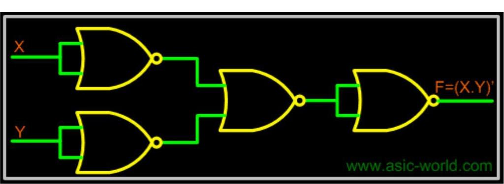
34 NAND NOR IMPLEMENTATIONS Universal gates are the ones which can be used for implementing any gate like AND, OR and NOT, or any combination of these basic gates; NAND and NOR gates are universal gates. But there are some rules that need to be followed when implementing NAND or NOR based gates. To facilitate the conversion to NAND and NOR logic, we have two new graphic symbols for these gates. NAND Gate
 form. Once logic function is converted to SOP, then is very easy to implement using NAND gate.")
35 NOR Gate Realization of logic function using NAND gates Any logic function can be implemented using NAND gates. To achieve this, first the logic function has to be written in Sum of Product (SOP) form. Once logic function is converted to SOP, then is very easy to implement using NAND gate. In other words any logic circuit with AND gates in first level and OR gates in second level can be converted into a NAND- NAND gate circuit. Consider the following SOP expression F = W.X.Y + X.Y.Z + Y.Z.W The above expression can be implemented with three AND gates in first stage and one OR gate in second stage as shown in figure. If bubbles are introduced at AND gates output and OR gates inputs (the same for NOR gates), the above circuit becomes as shown in figure. Now replace OR gate with input bubble with the NAND gate. Now we have circuit which is fully implemented with just NAND gates.

')' Idempotent = (XY) Involution Implementing OR using NAND gates Input Output Rule")
36 Realization of logic gates using NAND gates Implementing an inverter using NAND gate Input Output Rule (X.X)' = X' Idempotent Implementing AND using NAND gates Input Output Rule ((XY)'(XY)')' = ((XY)')' Idempotent = (XY) Involution Implementing OR using NAND gates Input Output Rule ((XX)'(YY)')' = (X'Y')' Idempotent = X''+Y'' DeMorgan = X+Y Involution


.")
37 Implementing NOR using NAND gates Input Output Rule ((XX)'(YY)')' =(X'Y')' Idempotent =X''+Y'' DeMorgan =X+Y Involution =(X+Y)' Idempotent Realization of logic function using NOR gates Any logic function can be implemented using NOR gates. To achieve this, first the logic function has to be written in Product of Sum (POS) form. Once it is converted to POS, then it's very easy to implement using NOR gate. In other words any logic circuit with OR gates in first level and AND gates in second level can be converted into a NOR-NOR gate circuit. Consider the following POS expression F = (X+Y). (Y+Z) The above expression can be implemented with three OR gates in first stage and one AND gate in second stage as shown in figure. If bubble are introduced at the output of the OR gates and the inputs of AND gate, the above circuit becomes as shown in figure.


38 Now replace AND gate with input bubble with the NOR gate. Now we have circuit which is fully implemented with just NOR gates. Realization of logic gates using NOR gates Implementing an inverter using NOR gate Input Output Rule (X+X)' = X' Idempotent Implementing AND using NOR gates Input Output Rule ((X+X)'+(Y+Y)')' =(X'+Y')' Idempotent = X''.Y'' DeMorgan = (X.Y) Involution
'+(X+Y)')' =")

39 Implementing OR using NOR gates Input Output Rule ((X+Y)'+(X+Y)')' = ((X+Y)')' Idempotent = X+Y Involution Implementing NAND using NOR gates Input Output Rule ((X+Y)'+(X+Y)')' = ((X+Y)')' Idempotent = X+Y Involution = (X+Y)' Idempotent
VALLIAMMAI ENGINEERING COLLEGE. SRM Nagar, Kattankulathur DEPARTMENT OF ELECTRONICS AND COMMUNICATION ENGINEERING EC6302 DIGITAL ELECTRONICS
 VALLIAMMAI ENGINEERING COLLEGE SRM Nagar, Kattankulathur-603 203 DEPARTMENT OF ELECTRONICS AND COMMUNICATION ENGINEERING EC6302 DIGITAL ELECTRONICS YEAR / SEMESTER: II / III ACADEMIC YEAR: 2015-2016 (ODD
B.Tech II Year I Semester (R13) Regular Examinations December 2014 DIGITAL LOGIC DESIGN
 Regular Examinations December 2014 DIGITAL LOGIC DESIGN") B.Tech II Year I Semester () Regular Examinations December 2014 (Common to IT and CSE) (a) If 1010 2 + 10 2 = X 10, then X is ----- Write the first 9 decimal digits in base 3. (c) What is meant by don
B.Tech II Year I Semester () Regular Examinations December 2014 (Common to IT and CSE) (a) If 1010 2 + 10 2 = X 10, then X is ----- Write the first 9 decimal digits in base 3. (c) What is meant by don
Code No: R Set No. 1
 Code No: R059210504 Set No. 1 II B.Tech I Semester Regular Examinations, November 2006 DIGITAL LOGIC DESIGN ( Common to Computer Science & Engineering, Information Technology and Computer Science & Systems
SIDDHARTH GROUP OF INSTITUTIONS :: PUTTUR Siddharth Nagar, Narayanavanam Road QUESTION BANK (DESCRIPTIVE)
") SIDDHARTH GROUP OF INSTITUTIONS :: PUTTUR Siddharth Nagar, Narayanavanam Road 517583 QUESTION BANK (DESCRIPTIVE) Subject with Code : STLD(16EC402) Year & Sem: II-B.Tech & I-Sem Course & Branch: B.Tech
SIDDHARTH GROUP OF INSTITUTIONS :: PUTTUR Siddharth Nagar, Narayanavanam Road 517583 QUESTION BANK (DESCRIPTIVE) Subject with Code : STLD(16EC402) Year & Sem: II-B.Tech & I-Sem Course & Branch: B.Tech
DHANALAKSHMI SRINIVASAN COLLEGE OF ENGINEERING AND TECHNOLOGY
 DHANALAKSHMI SRINIVASAN COLLEGE OF ENGINEERING AND TECHNOLOGY Dept/Sem: II CSE/03 DEPARTMENT OF ECE CS8351 DIGITAL PRINCIPLES AND SYSTEM DESIGN UNIT I BOOLEAN ALGEBRA AND LOGIC GATES PART A 1. How many
COLLEGE OF ENGINEERING DEPARTMENT OF ELECTRICAL AND ELECTRONICS ENGINEERING QUESTION BANK SUBJECT CODE & NAME: EC 1312 DIGITAL LOGIC CIRCUITS UNIT I
 KINGS COLLEGE OF ENGINEERING DEPARTMENT OF ELECTRICAL AND ELECTRONICS ENGINEERING QUESTION BANK SUBJECT CODE & NAME: EC 1312 DIGITAL LOGIC CIRCUITS YEAR / SEM: III / V UNIT I NUMBER SYSTEM & BOOLEAN ALGEBRA
BHARATHIDASAN ENGINEERING COLLEGE Degree / Branch : B.E./ECE Year / Sem : II/ III Sub.Code / Name : EC6302/DIGITAL ELECTRONICS
 BHARATHIDASAN ENGINEERING COLLEGE Degree / Branch : B.E./ECE Year / Sem : II/ III Sub.Code / Name : EC6302/DIGITAL ELECTRONICS FREQUENTLY ASKED QUESTIONS UNIT I MINIMIZATION TECHNIQUES AND LOGIC GATES
Code No: R Set No. 1
 Code No: R059210504 Set No. 1 II B.Tech I Semester Supplementary Examinations, February 2007 DIGITAL LOGIC DESIGN ( Common to Computer Science & Engineering, Information Technology and Computer Science
VALLIAMMAI ENGINEERING COLLEGE
 VALLIAMMAI ENGINEERING COLLEGE SRM Nagar, Kattankulathur 603 203 DEPARTMENT OF INFORMATION TECHNOLOGY & COMPUTER SCIENCE AND ENGINEERING QUESTION BANK II SEMESTER CS6201- DIGITAL PRINCIPLE AND SYSTEM DESIGN
Injntu.com Injntu.com Injntu.com R16
 1. a) What are the three methods of obtaining the 2 s complement of a given binary (3M) number? b) What do you mean by K-map? Name it advantages and disadvantages. (3M) c) Distinguish between a half-adder
(ii) Simplify and implement the following SOP function using NOR gates:
 Simplify and implement the following SOP function using NOR gates:") DHANALAKSHMI COLLEGE OF ENGINEERING DEPARTMENT OF ELECTRONICS AND COMMUNICATION ENGINEERING EE6301 DIGITAL LOGIC CIRCUITS UNIT I NUMBER SYSTEMS AND DIGITAL LOGIC FAMILIES PART A 1. How can an OR gate be
DHANALAKSHMI COLLEGE OF ENGINEERING DEPARTMENT OF ELECTRONICS AND COMMUNICATION ENGINEERING EE6301 DIGITAL LOGIC CIRCUITS UNIT I NUMBER SYSTEMS AND DIGITAL LOGIC FAMILIES PART A 1. How can an OR gate be
2.6 BOOLEAN FUNCTIONS
 2.6 BOOLEAN FUNCTIONS Binary variables have two values, either 0 or 1. A Boolean function is an expression formed with binary variables, the two binary operators AND and OR, one unary operator NOT, parentheses
VALLIAMMAI ENGINEERING COLLEGE
 VALLIAMMAI ENGINEERING COLLEGE SRM Nagar, Kattankulathur 603 203 DEPARTMENT OF INFORMATION TECHNOLOGY QUESTION BANK Academic Year 2018 19 III SEMESTER CS8351-DIGITAL PRINCIPLES AND SYSTEM DESIGN Regulation
Chapter 3 Simplification of Boolean functions
 3.1 Introduction Chapter 3 Simplification of Boolean functions In this chapter, we are going to discuss several methods for simplifying the Boolean function. What is the need for simplifying the Boolean
IT 201 Digital System Design Module II Notes
 IT 201 Digital System Design Module II Notes BOOLEAN OPERATIONS AND EXPRESSIONS Variable, complement, and literal are terms used in Boolean algebra. A variable is a symbol used to represent a logical quantity.
UNIT I BOOLEAN ALGEBRA AND COMBINATIONAL CIRCUITS PART-A (2 MARKS)
") SUBJECT NAME: DIGITAL LOGIC CIRCUITS YEAR / SEM : II / III DEPARTMENT : EEE UNIT I BOOLEAN ALGEBRA AND COMBINATIONAL CIRCUITS 1. What is variable mapping? 2. Name the two canonical forms for Boolean algebra.
SUBJECT NAME: DIGITAL LOGIC CIRCUITS YEAR / SEM : II / III DEPARTMENT : EEE UNIT I BOOLEAN ALGEBRA AND COMBINATIONAL CIRCUITS 1. What is variable mapping? 2. Name the two canonical forms for Boolean algebra.
R10. II B. Tech I Semester, Supplementary Examinations, May
 SET - 1 1. a) Convert the following decimal numbers into an equivalent binary numbers. i) 53.625 ii) 4097.188 iii) 167 iv) 0.4475 b) Add the following numbers using 2 s complement method. i) -48 and +31
Principles of Digital Techniques PDT (17320) Assignment No State advantages of digital system over analog system.
 Assignment No State advantages of digital system over analog system.") Assignment No. 1 1. State advantages of digital system over analog system. 2. Convert following numbers a. (138.56) 10 = (?) 2 = (?) 8 = (?) 16 b. (1110011.011) 2 = (?) 10 = (?) 8 = (?) 16 c. (3004.06)
Assignment No. 1 1. State advantages of digital system over analog system. 2. Convert following numbers a. (138.56) 10 = (?) 2 = (?) 8 = (?) 16 b. (1110011.011) 2 = (?) 10 = (?) 8 = (?) 16 c. (3004.06)
CONTENTS CHAPTER 1: NUMBER SYSTEM. Foreword...(vii) Preface... (ix) Acknowledgement... (xi) About the Author...(xxiii)
 Preface... (ix) Acknowledgement... (xi) About the Author...(xxiii)") CONTENTS Foreword...(vii) Preface... (ix) Acknowledgement... (xi) About the Author...(xxiii) CHAPTER 1: NUMBER SYSTEM 1.1 Digital Electronics... 1 1.1.1 Introduction... 1 1.1.2 Advantages of Digital Systems...
CONTENTS Foreword...(vii) Preface... (ix) Acknowledgement... (xi) About the Author...(xxiii) CHAPTER 1: NUMBER SYSTEM 1.1 Digital Electronics... 1 1.1.1 Introduction... 1 1.1.2 Advantages of Digital Systems...
HANSABA COLLEGE OF ENGINEERING & TECHNOLOGY (098) SUBJECT: DIGITAL ELECTRONICS ( ) Assignment
 SUBJECT: DIGITAL ELECTRONICS ( ) Assignment") Assignment 1. What is multiplexer? With logic circuit and function table explain the working of 4 to 1 line multiplexer. 2. Implement following Boolean function using 8: 1 multiplexer. F(A,B,C,D) = (2,3,5,7,8,9,12,13,14,15)
Assignment 1. What is multiplexer? With logic circuit and function table explain the working of 4 to 1 line multiplexer. 2. Implement following Boolean function using 8: 1 multiplexer. F(A,B,C,D) = (2,3,5,7,8,9,12,13,14,15)
 www.vidyarthiplus.com Question Paper Code : 31298 B.E./B.Tech. DEGREE EXAMINATION, NOVEMBER/DECEMBER 2013. Third Semester Computer Science and Engineering CS 2202/CS 34/EC 1206 A/10144 CS 303/080230012--DIGITAL
SHRI ANGALAMMAN COLLEGE OF ENGINEERING. (An ISO 9001:2008 Certified Institution) SIRUGANOOR, TIRUCHIRAPPALLI
 SIRUGANOOR, TIRUCHIRAPPALLI") SHRI ANGALAMMAN COLLEGE OF ENGINEERING AND TECHNOLOGY (An ISO 9001:2008 Certified Institution) SIRUGANOOR, TIRUCHIRAPPALLI 621 105 DEPARTMENT OF ELECTRONICS AND COMMUNICATION ENGINEERING EC1201 DIGITAL
SHRI ANGALAMMAN COLLEGE OF ENGINEERING AND TECHNOLOGY (An ISO 9001:2008 Certified Institution) SIRUGANOOR, TIRUCHIRAPPALLI 621 105 DEPARTMENT OF ELECTRONICS AND COMMUNICATION ENGINEERING EC1201 DIGITAL
Code No: 07A3EC03 Set No. 1
 Code No: 07A3EC03 Set No. 1 II B.Tech I Semester Regular Examinations, November 2008 SWITCHING THEORY AND LOGIC DESIGN ( Common to Electrical & Electronic Engineering, Electronics & Instrumentation Engineering,
KINGS COLLEGE OF ENGINEERING DEPARTMENT OF ELECTRICAL AND ELECTRONICS ENGINEERING QUESTION BANK NAME OF THE SUBJECT: EE 2255 DIGITAL LOGIC CIRCUITS
 KINGS COLLEGE OF ENGINEERING DEPARTMENT OF ELECTRICAL AND ELECTRONICS ENGINEERING QUESTION BANK NAME OF THE SUBJECT: EE 2255 DIGITAL LOGIC CIRCUITS YEAR / SEM: II / IV UNIT I BOOLEAN ALGEBRA AND COMBINATIONAL
Unit-IV Boolean Algebra
 Unit-IV Boolean Algebra Boolean Algebra Chapter: 08 Truth table: Truth table is a table, which represents all the possible values of logical variables/statements along with all the possible results of
SUBJECT CODE: IT T35 DIGITAL SYSTEM DESIGN YEAR / SEM : 2 / 3
 UNIT - I PART A (2 Marks) 1. Using Demorgan s theorem convert the following Boolean expression to an equivalent expression that has only OR and complement operations. Show the function can be implemented
Code No: R Set No. 1
 Code No: R059210504 Set No. 1 II B.Tech I Semester Regular Examinations, November 2007 DIGITAL LOGIC DESIGN ( Common to Computer Science & Engineering, Information Technology and Computer Science & Systems
Chapter 2 Boolean algebra and Logic Gates
 Chapter 2 Boolean algebra and Logic Gates 2. Introduction In working with logic relations in digital form, we need a set of rules for symbolic manipulation which will enable us to simplify complex expressions
CS8803: Advanced Digital Design for Embedded Hardware
 CS883: Advanced Digital Design for Embedded Hardware Lecture 2: Boolean Algebra, Gate Network, and Combinational Blocks Instructor: Sung Kyu Lim (limsk@ece.gatech.edu) Website: http://users.ece.gatech.edu/limsk/course/cs883
Chapter 2. Boolean Expressions:
 Chapter 2 Boolean Expressions: A Boolean expression or a function is an expression which consists of binary variables joined by the Boolean connectives AND and OR along with NOT operation. Any Boolean
END-TERM EXAMINATION
 (Please Write your Exam Roll No. immediately) END-TERM EXAMINATION DECEMBER 2006 Exam. Roll No... Exam Series code: 100919DEC06200963 Paper Code: MCA-103 Subject: Digital Electronics Time: 3 Hours Maximum
CHAPTER-2 STRUCTURE OF BOOLEAN FUNCTION USING GATES, K-Map and Quine-McCluskey
 CHAPTER-2 STRUCTURE OF BOOLEAN FUNCTION USING GATES, K-Map and Quine-McCluskey 2. Introduction Logic gates are connected together to produce a specified output for certain specified combinations of input
1. Mark the correct statement(s)
") 1. Mark the correct statement(s) 1.1 A theorem in Boolean algebra: a) Can easily be proved by e.g. logic induction b) Is a logical statement that is assumed to be true, c) Can be contradicted by another
1. Mark the correct statement(s) 1.1 A theorem in Boolean algebra: a) Can easily be proved by e.g. logic induction b) Is a logical statement that is assumed to be true, c) Can be contradicted by another
Module -7. Karnaugh Maps
 1 Module -7 Karnaugh Maps 1. Introduction 2. Canonical and Standard forms 2.1 Minterms 2.2 Maxterms 2.3 Canonical Sum of Product or Sum-of-Minterms (SOM) 2.4 Canonical product of sum or Product-of-Maxterms(POM)
DKT 122/3 DIGITAL SYSTEM 1
 Company LOGO DKT 122/3 DIGITAL SYSTEM 1 BOOLEAN ALGEBRA (PART 2) Boolean Algebra Contents Boolean Operations & Expression Laws & Rules of Boolean algebra DeMorgan s Theorems Boolean analysis of logic circuits
X Y Z F=X+Y+Z
 This circuit is used to obtain the compliment of a value. If X = 0, then X = 1. The truth table for NOT gate is : X X 0 1 1 0 2. OR gate : The OR gate has two or more input signals but only one output
R a) Simplify the logic functions from binary to seven segment display code converter (8M) b) Simplify the following using Tabular method
 Simplify the logic functions from binary to seven segment display code converter (8M) b) Simplify the following using Tabular method") SET - 1 1. a) Convert the decimal number 250.5 to base 3, base 4 b) Write and prove de-morgan laws c) Implement two input EX-OR gate from 2 to 1 multiplexer (3M) d) Write the demerits of PROM (3M) e) What
SET - 1 1. a) Convert the decimal number 250.5 to base 3, base 4 b) Write and prove de-morgan laws c) Implement two input EX-OR gate from 2 to 1 multiplexer (3M) d) Write the demerits of PROM (3M) e) What
INSTITUTE OF AERONAUTICAL ENGINEERING (Autonomous) Dundigal, Hyderabad
 Dundigal, Hyderabad") INSTITUTE OF AERONAUTICAL ENGINEERING (Autonomous) Dundigal, Hyderabad - 500043 Course Name : DIGITAL LOGIC DESISN Course Code : AEC020 Class : B Tech III Semester Branch : CSE Academic Year : 2018 2019
INSTITUTE OF AERONAUTICAL ENGINEERING (Autonomous) Dundigal, Hyderabad - 500043 Course Name : DIGITAL LOGIC DESISN Course Code : AEC020 Class : B Tech III Semester Branch : CSE Academic Year : 2018 2019
Digital logic fundamentals. Question Bank. Unit I
 Digital logic fundamentals Question Bank Subject Name : Digital Logic Fundamentals Subject code: CA102T Staff Name: R.Roseline Unit I 1. What is Number system? 2. Define binary logic. 3. Show how negative
Switching Theory & Logic Design/Digital Logic Design Question Bank
 Switching Theory & Logic Design/Digital Logic Design Question Bank UNIT I NUMBER SYSTEMS AND CODES 1. A 12-bit Hamming code word containing 8-bits of data and 4 parity bits is read from memory. What was
10EC33: DIGITAL ELECTRONICS QUESTION BANK
 10EC33: DIGITAL ELECTRONICS Faculty: Dr.Bajarangbali E Examination QuestionS QUESTION BANK 1. Discuss canonical & standard forms of Boolean functions with an example. 2. Convert the following Boolean function
INSTITUTE OF AERONAUTICAL ENGINEERING (Autonomous) Dundigal, Hyderabad
 Dundigal, Hyderabad") INSTITUTE OF AERONAUTICAL ENGINEERING (Autonomous) Dundigal, Hyderabad - 500 043 COMPUTER SCIENCE AND ENGINEERING TUTORIAL QUESTION BANK Name : DIGITAL LOGIC DESISN Code : AEC020 Class : B Tech III Semester
INSTITUTE OF AERONAUTICAL ENGINEERING (Autonomous) Dundigal, Hyderabad - 500 043 COMPUTER SCIENCE AND ENGINEERING TUTORIAL QUESTION BANK Name : DIGITAL LOGIC DESISN Code : AEC020 Class : B Tech III Semester
Computer Organization
 Computer Organization (Logic circuits design and minimization) KR Chowdhary Professor & Head Email: kr.chowdhary@gmail.com webpage: krchowdhary.com Department of Computer Science and Engineering MBM Engineering
Philadelphia University Faculty of Information Technology Department of Computer Science. Computer Logic Design. By Dareen Hamoudeh.
 Philadelphia University Faculty of Information Technology Department of Computer Science Computer Logic Design By Dareen Hamoudeh Dareen Hamoudeh 1 Canonical Forms (Standard Forms of Expression) Minterms
Experiment 4 Boolean Functions Implementation
 Experiment 4 Boolean Functions Implementation Introduction: Generally you will find that the basic logic functions AND, OR, NAND, NOR, and NOT are not sufficient to implement complex digital logic functions.
COPYRIGHTED MATERIAL INDEX
 INDEX Absorption law, 31, 38 Acyclic graph, 35 tree, 36 Addition operators, in VHDL (VHSIC hardware description language), 192 Algebraic division, 105 AND gate, 48 49 Antisymmetric, 34 Applicable input
SIR C.R.REDDY COLLEGE OF ENGINEERING, ELURU DEPARTMENT OF INFORMATION TECHNOLOGY LESSON PLAN
 SIR C.R.REDDY COLLEGE OF ENGINEERING, ELURU DEPARTMENT OF INFORMATION TECHNOLOGY LESSON PLAN SUBJECT: CSE 2.1.6 DIGITAL LOGIC DESIGN CLASS: 2/4 B.Tech., I SEMESTER, A.Y.2017-18 INSTRUCTOR: Sri A.M.K.KANNA
NADAR SARASWATHI COLLEGE OF ENGINEERING AND TECHNOLOGY Vadapudupatti, Theni
 NADAR SARASWATHI COLLEGE OF ENGINEERING AND TECHNOLOGY Vadapudupatti, Theni-625531 Question Bank for the Units I to V SEMESTER BRANCH SUB CODE 3rd Semester B.E. / B.Tech. Electrical and Electronics Engineering
II/IV B.Tech (Regular/Supplementary) DEGREE EXAMINATION. Answer ONE question from each unit.
 DEGREE EXAMINATION. Answer ONE question from each unit.") Hall Ticket Number: 14CS IT303 November, 2017 Third Semester Time: Three Hours Answer Question No.1 compulsorily. II/IV B.Tech (Regular/Supplementary) DEGREE EXAMINATION Common for CSE & IT Digital Logic
Hall Ticket Number: 14CS IT303 November, 2017 Third Semester Time: Three Hours Answer Question No.1 compulsorily. II/IV B.Tech (Regular/Supplementary) DEGREE EXAMINATION Common for CSE & IT Digital Logic
ELCT201: DIGITAL LOGIC DESIGN
 ELCT201: DIGITAL LOGIC DESIGN Dr. Eng. Haitham Omran, haitham.omran@guc.edu.eg Dr. Eng. Wassim Alexan, wassim.joseph@guc.edu.eg Lecture 3 Following the slides of Dr. Ahmed H. Madian ذو الحجة 1438 ه Winter
Combinational Logic & Circuits
 Week-I Combinational Logic & Circuits Spring' 232 - Logic Design Page Overview Binary logic operations and gates Switching algebra Algebraic Minimization Standard forms Karnaugh Map Minimization Other
ELCT201: DIGITAL LOGIC DESIGN
 ELCT201: DIGITAL LOGIC DESIGN Dr. Eng. Haitham Omran, haitham.omran@guc.edu.eg Dr. Eng. Wassim Alexan, wassim.joseph@guc.edu.eg Lecture 3 Following the slides of Dr. Ahmed H. Madian محرم 1439 ه Winter
Computer Science. Unit-4: Introduction to Boolean Algebra
 Unit-4: Introduction to Boolean Algebra Learning Objective At the end of the chapter students will: Learn Fundamental concepts and basic laws of Boolean algebra. Learn about Boolean expression and will
DIGITAL ELECTRONICS. Vayu Education of India
 DIGITAL ELECTRONICS ARUN RANA Assistant Professor Department of Electronics & Communication Engineering Doon Valley Institute of Engineering & Technology Karnal, Haryana (An ISO 9001:2008 ) Vayu Education
ENGINEERS ACADEMY. 7. Given Boolean theorem. (a) A B A C B C A B A C. (b) AB AC BC AB BC. (c) AB AC BC A B A C B C.
 A B A C B C A B A C. (b) AB AC BC AB BC. (c) AB AC BC A B A C B C.") Digital Electronics Boolean Function QUESTION BANK. The Boolean equation Y = C + C + C can be simplified to (a) (c) A (B + C) (b) AC (d) C. The Boolean equation Y = (A + B) (A + B) can be simplified to
Digital Electronics Boolean Function QUESTION BANK. The Boolean equation Y = C + C + C can be simplified to (a) (c) A (B + C) (b) AC (d) C. The Boolean equation Y = (A + B) (A + B) can be simplified to
Chapter 3. Gate-Level Minimization. Outlines
 Chapter 3 Gate-Level Minimization Introduction The Map Method Four-Variable Map Five-Variable Map Outlines Product of Sums Simplification Don t-care Conditions NAND and NOR Implementation Other Two-Level
CS470: Computer Architecture. AMD Quad Core
 CS470: Computer Architecture Yashwant K. Malaiya, Professor malaiya@cs.colostate.edu AMD Quad Core 1 Architecture Layers Building blocks Gates, flip-flops Functional bocks: Combinational, Sequential Instruction
Combinational Logic Circuits
 Chapter 2 Combinational Logic Circuits J.J. Shann (Slightly trimmed by C.P. Chung) Chapter Overview 2-1 Binary Logic and Gates 2-2 Boolean Algebra 2-3 Standard Forms 2-4 Two-Level Circuit Optimization
Gate Level Minimization
 Gate Level Minimization By Dr. M. Hebaishy Digital Logic Design Ch- Simplifying Boolean Equations Example : Y = AB + AB Example 2: = B (A + A) T8 = B () T5 = B T Y = A(AB + ABC) = A (AB ( + C ) ) T8 =
Boolean Algebra and Logic Gates
 Boolean Algebra and Logic Gates Binary logic is used in all of today's digital computers and devices Cost of the circuits is an important factor Finding simpler and cheaper but equivalent circuits can
Assignment (3-6) Boolean Algebra and Logic Simplification - General Questions
 Boolean Algebra and Logic Simplification - General Questions") Assignment (3-6) Boolean Algebra and Logic Simplification - General Questions 1. Convert the following SOP expression to an equivalent POS expression. 2. Determine the values of A, B, C, and D that make
Assignment (3-6) Boolean Algebra and Logic Simplification - General Questions 1. Convert the following SOP expression to an equivalent POS expression. 2. Determine the values of A, B, C, and D that make
SWITCHING THEORY AND LOGIC CIRCUITS
 SWITCHING THEORY AND LOGIC CIRCUITS COURSE OBJECTIVES. To understand the concepts and techniques associated with the number systems and codes 2. To understand the simplification methods (Boolean algebra
PROGRAMMABLE LOGIC DEVICES
 PROGRAMMABLE LOGIC DEVICES Programmable logic devices (PLDs) are used for designing logic circuits. PLDs can be configured by the user to perform specific functions. The different types of PLDs available
Hours / 100 Marks Seat No.
 17333 13141 3 Hours / 100 Seat No. Instructions (1) All Questions are Compulsory. (2) Answer each next main Question on a new page. (3) Illustrate your answers with neat sketches wherever necessary. (4)
Binary logic. Dr.Abu-Arqoub
 Binary logic Binary logic deals with variables like (a, b, c,, x, y) that take on two discrete values (, ) and with operations that assume logic meaning ( AND, OR, NOT) Truth table is a table of all possible
 Class Subject Code Subject Prepared By Lesson Plan for Time: Lesson. No 1.CONTENT LIST: Introduction to UnitI 2. SKILLS ADDRESSED: Listening I year, 02 sem CS6201 Digital Principles & System Design S.Seedhanadevi
APPENDIX A SHORT QUESTIONS AND ANSWERS
 APPENDIX A SHORT QUESTIONS AND ANSWERS Unit I Boolean Algebra and Logic Gates Part - A 1. Define binary logic? Binary logic consists of binary variables and logical operations. The variables are designated
Scheme G. Sample Test Paper-I
 Sample Test Paper-I Marks : 25 Times:1 Hour 1. All questions are compulsory. 2. Illustrate your answers with neat sketches wherever necessary. 3. Figures to the right indicate full marks. 4. Assume suitable
R07
 www..com www..com SET - 1 II B. Tech I Semester Supplementary Examinations May 2013 SWITCHING THEORY AND LOGIC DESIGN (Com. to EEE, EIE, BME, ECC) Time: 3 hours Max. Marks: 80 Answer any FIVE Questions
Gate Level Minimization Map Method
 Gate Level Minimization Map Method Complexity of hardware implementation is directly related to the complexity of the algebraic expression Truth table representation of a function is unique Algebraically
CS6201-DIGITAL PRINCIPLE AND SYSTEM DESIGN I YEAR/II SEM PART-B UNIT-I BOOLEAN ALGEBRA AND LOGIC GATES.
 CS6201-DIGITAL PRINCIPLE AND SYSTEM DESIGN I YEAR/II SEM PART-B UNIT-I BOOLEAN ALGEBRA AND LOGIC GATES. 1) Simplify the boolean function using tabulation method. F = (0, 1, 2, 8, 10, 11, 14, 15) List all
R07. Code No: V0423. II B. Tech II Semester, Supplementary Examinations, April
 SET - 1 II B. Tech II Semester, Supplementary Examinations, April - 2012 SWITCHING THEORY AND LOGIC DESIGN (Electronics and Communications Engineering) Time: 3 hours Max Marks: 80 Answer any FIVE Questions
 Get Free notes at Module-I One s Complement: Complement all the bits.i.e. makes all 1s as 0s and all 0s as 1s Two s Complement: One s complement+1 SIGNED BINARY NUMBERS Positive integers (including zero)
2.1 Binary Logic and Gates
 1 EED2003 Digital Design Presentation 2: Boolean Algebra Asst. Prof.Dr. Ahmet ÖZKURT Asst. Prof.Dr Hakkı T. YALAZAN Based on the Lecture Notes by Jaeyoung Choi choi@comp.ssu.ac.kr Fall 2000 2.1 Binary
Incompletely Specified Functions with Don t Cares 2-Level Transformation Review Boolean Cube Karnaugh-Map Representation and Methods Examples
 Lecture B: Logic Minimization Incompletely Specified Functions with Don t Cares 2-Level Transformation Review Boolean Cube Karnaugh-Map Representation and Methods Examples Incompletely specified functions
Lecture (05) Boolean Algebra and Logic Gates
 Boolean Algebra and Logic Gates") Lecture (05) Boolean Algebra and Logic Gates By: Dr. Ahmed ElShafee ١ Minterms and Maxterms consider two binary variables x and y combined with an AND operation. Since eachv ariable may appear in either
Lecture (05) Boolean Algebra and Logic Gates By: Dr. Ahmed ElShafee ١ Minterms and Maxterms consider two binary variables x and y combined with an AND operation. Since eachv ariable may appear in either
Gate-Level Minimization. BME208 Logic Circuits Yalçın İŞLER
 Gate-Level Minimization BME28 Logic Circuits Yalçın İŞLER islerya@yahoo.com http://me.islerya.com Complexity of Digital Circuits Directly related to the complexity of the algebraic expression we use to
Digital Logic Design (CEN-120) (3+1)
 (3+1)") Digital Logic Design (CEN-120) (3+1) ASSISTANT PROFESSOR Engr. Syed Rizwan Ali, MS(CAAD)UK, PDG(CS)UK, PGD(PM)IR, BS(CE)PK HEC Certified Master Trainer (MT-FPDP) PEC Certified Professional Engineer (COM/2531)
Digital Logic Design (CEN-120) (3+1) ASSISTANT PROFESSOR Engr. Syed Rizwan Ali, MS(CAAD)UK, PDG(CS)UK, PGD(PM)IR, BS(CE)PK HEC Certified Master Trainer (MT-FPDP) PEC Certified Professional Engineer (COM/2531)
UNIT-4 BOOLEAN LOGIC. NOT Operator Operates on single variable. It gives the complement value of variable.
 UNIT-4 BOOLEAN LOGIC Boolean algebra is an algebra that deals with Boolean values((true and FALSE). Everyday we have to make logic decisions: Should I carry the book or not?, Should I watch TV or not?
UNIT II. Circuit minimization
 UNIT II Circuit minimization The complexity of the digital logic gates that implement a Boolean function is directly related to the complexity of the algebraic expression from which the function is implemented.
KING FAHD UNIVERSITY OF PETROLEUM & MINERALS COMPUTER ENGINEERING DEPARTMENT
 KING FAHD UNIVERSITY OF PETROLEUM & MINERALS COMPUTER ENGINEERING DEPARTMENT COE 202: Digital Logic Design Term 162 (Spring 2017) Instructor: Dr. Abdulaziz Barnawi Class time: U.T.R.: 11:00-11:50AM Class
CMPE223/CMSE222 Digital Logic
 CMPE223/CMSE222 Digital Logic Optimized Implementation of Logic Functions: Strategy for Minimization, Minimum Product-of-Sums Forms, Incompletely Specified Functions Terminology For a given term, each
Chapter 2: Combinational Systems
 Uchechukwu Ofoegbu Chapter 2: Combinational Systems Temple University Adapted from Alan Marcovitz s Introduction to Logic and Computer Design Riddle Four switches can be turned on or off. One is the switch
Specifying logic functions
 CSE4: Components and Design Techniques for Digital Systems Specifying logic functions Instructor: Mohsen Imani Slides from: Prof.Tajana Simunic and Dr.Pietro Mercati We have seen various concepts: Last
2008 The McGraw-Hill Companies, Inc. All rights reserved.
 28 The McGraw-Hill Companies, Inc. All rights reserved. 28 The McGraw-Hill Companies, Inc. All rights reserved. All or Nothing Gate Boolean Expression: A B = Y Truth Table (ee next slide) or AB = Y 28
MGU-BCA-205- Second Sem- Core VI- Fundamentals of Digital Systems- MCQ s. 2. Why the decimal number system is also called as positional number system?
 MGU-BCA-205- Second Sem- Core VI- Fundamentals of Digital Systems- MCQ s Unit-1 Number Systems 1. What does a decimal number represents? A. Quality B. Quantity C. Position D. None of the above 2. Why the
3. The high voltage level of a digital signal in positive logic is : a) 1 b) 0 c) either 1 or 0
 1 b) 0 c) either 1 or 0") 1. The number of level in a digital signal is: a) one b) two c) four d) ten 2. A pure sine wave is : a) a digital signal b) analog signal c) can be digital or analog signal d) neither digital nor analog
1. The number of level in a digital signal is: a) one b) two c) four d) ten 2. A pure sine wave is : a) a digital signal b) analog signal c) can be digital or analog signal d) neither digital nor analog
Experiment 3: Logic Simplification
 Module: Logic Design Name:... University no:.. Group no:. Lab Partner Name: Mr. Mohamed El-Saied Experiment : Logic Simplification Objective: How to implement and verify the operation of the logical functions
LSN 4 Boolean Algebra & Logic Simplification. ECT 224 Digital Computer Fundamentals. Department of Engineering Technology
 LSN 4 Boolean Algebra & Logic Simplification Department of Engineering Technology LSN 4 Key Terms Variable: a symbol used to represent a logic quantity Compliment: the inverse of a variable Literal: a
Gate-Level Minimization
 Gate-Level Minimization ( 范倫達 ), Ph. D. Department of Computer Science National Chiao Tung University Taiwan, R.O.C. Fall, 2017 ldvan@cs.nctu.edu.tw http://www.cs.nctu.edu.tw/~ldvan/ Outlines The Map Method
Gate-Level Minimization
 Gate-Level Minimization ( 范倫達 ), Ph. D. Department of Computer Science National Chiao Tung University Taiwan, R.O.C. Fall, 2011 ldvan@cs.nctu.edu.tw http://www.cs.nctu.edu.tw/~ldvan/ Outlines The Map Method
Combinational Logic Circuits
 Chapter 3 Combinational Logic Circuits 12 Hours 24 Marks 3.1 Standard representation for logical functions Boolean expressions / logic expressions / logical functions are expressed in terms of logical
QUESTION BANK FOR TEST
 CSCI 2121 Computer Organization and Assembly Language PRACTICE QUESTION BANK FOR TEST 1 Note: This represents a sample set. Please study all the topics from the lecture notes. Question 1. Multiple Choice
ECE380 Digital Logic
 ECE38 Digital Logic Optimized Implementation of Logic Functions: Strategy for Minimization, Minimum Product-of-Sums Forms, Incompletely Specified Functions Dr. D. J. Jackson Lecture 8- Terminology For
PART B. 3. Minimize the following function using K-map and also verify through tabulation method. F (A, B, C, D) = +d (0, 3, 6, 10).
 = +d (0, 3, 6, 10).") II B. Tech II Semester Regular Examinations, May/June 2015 SWITCHING THEORY AND LOGIC DESIGN (Com. to EEE, ECE, ECC, EIE.) Time: 3 hours Max. Marks: 70 Note: 1. Question Paper consists of two parts (Part-A
II B. Tech II Semester Regular Examinations, May/June 2015 SWITCHING THEORY AND LOGIC DESIGN (Com. to EEE, ECE, ECC, EIE.) Time: 3 hours Max. Marks: 70 Note: 1. Question Paper consists of two parts (Part-A
Summary. Boolean Addition
 Summary Boolean Addition In Boolean algebra, a variable is a symbol used to represent an action, a condition, or data. A single variable can only have a value of or 0. The complement represents the inverse
Boolean Algebra. BME208 Logic Circuits Yalçın İŞLER
 Boolean Algebra BME28 Logic Circuits Yalçın İŞLER islerya@yahoo.com http://me.islerya.com 5 Boolean Algebra /2 A set of elements B There exist at least two elements x, y B s. t. x y Binary operators: +
Review. EECS Components and Design Techniques for Digital Systems. Lec 05 Boolean Logic 9/4-04. Seq. Circuit Behavior. Outline.
 Review EECS 150 - Components and Design Techniques for Digital Systems Lec 05 Boolean Logic 94-04 David Culler Electrical Engineering and Computer Sciences University of California, Berkeley Design flow
Chapter 2 Combinational Logic Circuits
 Logic and Computer Design Fundamentals Chapter 2 Combinational Logic Circuits Part 2 Circuit Optimization Overview Part Gate Circuits and Boolean Equations Binary Logic and Gates Boolean Algebra Standard
BOOLEAN ALGEBRA. Logic circuit: 1. From logic circuit to Boolean expression. Derive the Boolean expression for the following circuits.
 COURSE / CODE DIGITAL SYSTEMS FUNDAMENTAL (ECE 421) DIGITAL ELECTRONICS FUNDAMENTAL (ECE 422) BOOLEAN ALGEBRA Boolean Logic Boolean logic is a complete system for logical operations. It is used in countless