High speed full wafer monitoring of surface, edge and bonding interface for 3D-stacking
|
|
|
- Julianna Simpson
- 6 years ago
- Views:
Transcription

1 Sematech Workshop on 3D Interconnect Metrology Sematech Workshop on 3D Interconnect Metrology, July High speed full wafer monitoring of surface, edge and bonding interface for 3D-stacking Lars Markwort, Pierre-Yves Guittet, Greg Savage, Christoph Kappel Nanda Tech GmbH Anne Jourdain, Sandip Halder imec Eleonora Storace SUSS 1
2 Agenda Introduction Applications previously o o o Edge inspection Post-grinding inspection Post-recess etch inspection Applications update o o o Bond Layer inspection Post-grinding inspection Post-recess etch inspection Summary 2


3 Nanda Tech SPARK Technology Basics New Technology: No moving parts Full wafer illumination and imaging Illuminate and capture full wafer at once Design for stability & tool-to-tool matching Maximize throughput at highest sensitivity Key technology features Reflected & scattered channels Full wafer inspection in seconds Three inspection channels: Visible darkfield Visible brightfield NIR Large depth of focus inspect single or multiple bonded wafers w/o autofocus Vis/IR for surface and sub-surface defect detection Edge inspection 3

4 Combined Reflected & Scattered Light Inspection Capture reflected and scattered light images for every wafer See complementary defects in the two channels Combined analysis increases chance to detect Defects of Interest Example: Post-Grinding Inspection Reflected Scattered 4
 TSV Formation BEOL (Passivation, Poly-Imide) Bonding Thinning Backside Processing Device Wafer Carrier Wafer Incoming inspection")
5 Nanda in 3D Process Flow TSV formation and temporary Bonding/Thinning inspection is critical to ensure wafer-to-wafer (W2W) high yield Nanda Spark can cover a wide range of 3D integration processes on silicon and glass carriers FEOL (Frontside, Backside, Edge) TSV Formation BEOL (Passivation, Poly-Imide) Bonding Thinning Backside Processing Device Wafer Carrier Wafer Incoming inspection Particle check Edge Trimming Temp Glue spinning Clean Check Temp Glue defects Wafer to Carrier Temp bonding Wafer thinning By grinding Grinding damage Removal & clean Dry Etch (TSV exposed) CVD Debond 5


6 Bond Layer Inspection Through Si Carrier Large depth of focus: No focus adjustment needed o Inspect full thickness and thinned bonded wafer pairs Distinguish different types of bonding layer defects: o Air bubbles, embedded particles, delamination Device Wafer Carrier Wafer Nanda one-shot NIR full wafer inspection: 30 s high resolution, high contrast Fully automated, atmospheric inspection Scanning Accoustic Microscope: 30 minutes high resolution but low contrast Requires manual loading into water bath 6


7 Bond Layer Inspection Through Si Carrier Detect: Re-flow of adhesive material during grinding Prethinning Wafer 1 Wafer 2 Localized thickness variations due to particles and/or bubbles Device Wafer Device Wafer Carrier Wafer Carrier Wafer Postthinning Device Wafer Wafer 3 Wafer 4 Interference fringes due to large area thickness variations Carrier Wafer 7


8 Image Gallery Post Grind Brightfield and Darkfield image gallery of surface defects Nanda Brightfield 1 2 Nanda Darkfield
 Thinned wafer center shifted (sinusoidal curve)")
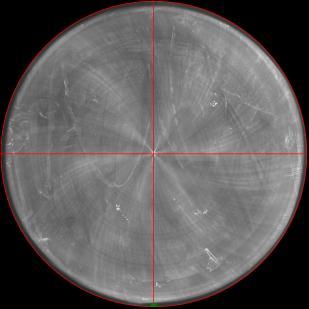
9 Topography & Edge Analysis Large dimples and edge topography detected on thinned wafer Edge analysis: [um] [um] Mercator plot 0) Thinned wafer center shifted (sinusoidal curve) 9


![Thinned Si TTV Glue TTV Glue Mean/ TTV [um] Thin silicon](/docs-images/80/82256552/images/10-2.jpg "Mean/ TTV [um] Bow/ Warp 43.44/ 14.86 90.50/ 12.987 47.")
10 Automated Defect Inspection, TTV & Bow/Warp Nanda full wafer brightfield + local small field-of-view metrology Brightfield Wafer Bow Thinned silicon wafer topography seen in Nanda brightfield is caused by glue layer TTV Thinned Si TTV Glue TTV Glue Mean/ TTV [um] Thin silicon Mean/ TTV [um] Bow/ Warp 43.44/ / /


11 Brightfield NIR Sematech Workshop on 3D Interconnect Metrology, July Combination Full Wafer BF and NIR Inspection NIR images identifies voids at location of dimple surface defect detected in brightfield images Slot 1 Visible Brightfield Images Slot 2 NIR Images Shows voids at location of dimples seen in Brightfield Slot 1 Slot 2 Slot 9 Slot 10 Slot 9 Slot 10 11


12 SAM vs. Nanda Surface and Bond Layer Inspection SAM Inspection Nanda Tech Brightfield Inspection Nanda Tech NIR Inspection TTV Data 12
13 Bond Layer Inspection Through Si Carrier Carrier Wafer Side DRAM product wafer bonded to Si carrier Carrier Wafer Side Nanda Tech NIR Inspection Void detection 30s integration time SAM Inspection for voids High Resolution Scans 40 min scan time 13


14 Through Si Carrier Bond Layer Void Inspection Carrier Wafer Side SAM Inspection Void High Resolution Scan Nanda Tech NIR Inspection Detected Voids 14


15 Combination of Unique Capabilities for 3D/TSV Sematech Workshop on 3D Interconnect Metrology, July Post-Grinding: BF inspection of dimples, grinding topography, chipping & edge Post-Grinding: DF inspection of residual silicon thickness & exposed Cu vias Post-Bonding: NIR Inspection of voids, delamination & embedded particles Dimples Bond layer inclusion & voids Delamination Exposed Cu nails Bow/Warp Glue Layer TTV Large scale defects often missed by traditional inspection 15
 loops o Feedforward to")
16 Summary Nanda provides control solution for TSV processes in R&D and production Automatic classification of critical vs. non-critical defects High Throughput 100% lot/wafers/dies inspection Low cost of ownership Lowest $ spent per measured wafer Use Nanda data for Advanced Process Control (APC) loops o Feedforward to recess etch o Feedback loop to Bonder/Grinder/TSV etch Nanda Spark module can be directly integrated into bonder, de-bonder, grinder FEOL & BEOL TSV Formation Back-End Bonding Thinning Backside processing CD, density Defectivity Depth, Profile Incoming inspection Device Trimming Bonding quality Wafer to Wafer alignment Wafer edge defects Post-Grinding Clean Particles, Dimples, Copper Nail Exposure, Delamination, Edge, Particles in Glue Recess Etch Particles, Scratches, Edge, Exposed Copper Nails 16
Bringing 3D Integration to Packaging Mainstream
 Bringing 3D Integration to Packaging Mainstream Enabling a Microelectronic World MEPTEC Nov 2012 Choon Lee Technology HQ, Amkor Highlighted TSV in Packaging TSMC reveals plan for 3DIC design based on silicon
Case Studies of All-Surface Inspection in a 3DI-TSV R&D Environment. Rolf Shervey Sr. Applications Engineer Rudolph Technologies, Inc.
 Case Studies of All-Surface Inspection in a 3DI-TSV R&D Environment Rolf Shervey Sr. Applications Engineer Rudolph Technologies, Inc. Equipment in Albany Explorer Inspection Cluster AXi 935 for top surface
3D SYSTEM INTEGRATION TECHNOLOGY CHOICES AND CHALLENGE ERIC BEYNE, ANTONIO LA MANNA
 3D SYSTEM INTEGRATION TECHNOLOGY CHOICES AND CHALLENGE ERIC BEYNE, ANTONIO LA MANNA OUTLINE 3D Application Drivers and Roadmap 3D Stacked-IC Technology 3D System-on-Chip: Fine grain partitioning Conclusion
Total Inspection Solutions Ensuring Known-Good 3DIC Package. Nevo Laron, Camtek USA, Santa Clara, CA
 Total Inspection Solutions Ensuring Known-Good 3DIC Package Nevo Laron, Camtek USA, Santa Clara, CA Density Packaging Trends vs. Defect Costs Functionality Package Yield 3DIC yield statistics 101 1.00
Scanning Acoustic Microscopy For Metrology of 3D Interconnect Bonded Wafers
 Scanning Acoustic Microscopy For Metrology of 3D Interconnect Bonded Wafers Jim McKeon, Ph.D. - Sonix, Director of Technology Sriram Gopalan, Ph.D. - Sonix, Technology Engineer 8700 Morrissette Drive 8700
Metrology for Characterization of Wafer Thickness Uniformity During 3D-IC Processing. SEMATECH Workshop on 3D Interconnect Metrology
 Metrology for Characterization of Wafer Thickness Uniformity During 3D-IC Processing SEMATECH Workshop on 3D Interconnect Metrology Chris Lee July 11, 2012 Outline Introduction Motivation For New Metrology
OPTICAL TECHNOLOGIES FOR TSV INSPECTION Arun A. Aiyer, Frontier Semiconductor 2127 Ringwood Ave, San Jose, California 95131
 OPTICAL TECHNOLOGIES FOR TSV INSPECTION Arun A. Aiyer, Frontier Semiconductor 2127 Ringwood Ave, San Jose, California 95131 ABSTRACT: In this paper, Frontier Semiconductor will introduce a new technology
Known-Good-Die (KGD) Wafer-Level Packaging (WLP) Inspection Tutorial
 Wafer-Level Packaging (WLP) Inspection Tutorial") Known-Good-Die (KGD) Wafer-Level Packaging (WLP) Inspection Tutorial Approach to Inspection Wafer inspection process starts with detecting defects and ends with making a decision on what to do with both
Known-Good-Die (KGD) Wafer-Level Packaging (WLP) Inspection Tutorial Approach to Inspection Wafer inspection process starts with detecting defects and ends with making a decision on what to do with both
From 3D Toolbox to 3D Integration: Examples of Successful 3D Applicative Demonstrators N.Sillon. CEA. All rights reserved
 From 3D Toolbox to 3D Integration: Examples of Successful 3D Applicative Demonstrators N.Sillon Agenda Introduction 2,5D: Silicon Interposer 3DIC: Wide I/O Memory-On-Logic 3D Packaging: X-Ray sensor Conclusion
LITHOGRAPHY CHALLENGES FOR LEADING EDGE 3D PACKAGING APPLICATIONS
 LITHOGRAPHY CHALLENGES FOR LEADING EDGE 3D PACKAGING APPLICATIONS Warren W. Flack, Manish Ranjan, Gareth Kenyon, Robert Hsieh Ultratech, Inc. 3050 Zanker Road, San Jose, CA 95134 USA mranjan@ultratech.com
Embedded UTCP interposers for miniature smart sensors
 Embedded UTCP interposers for miniature smart sensors T. Sterken 1,2, M. Op de Beeck 2, Tom Torfs 2, F. Vermeiren 1,2, C. Van Hoof 2, J. Vanfleteren 1,2 1 CMST (affiliated with Ugent and IMEC), Technologiepark
3D SoC and Heterogeneous Integrations
 3D SoC and Heterogeneous Integrations Content Introduction ST positioning Why 3D-Integration? CMOS Imager Sensor: the TSV success story! 3D SOC technology & applications Via Middle FE integrations Back-side
Comparison & highlight on the last 3D TSV technologies trends Romain Fraux
 Comparison & highlight on the last 3D TSV technologies trends Romain Fraux Advanced Packaging & MEMS Project Manager European 3D Summit 18 20 January, 2016 Outline About System Plus Consulting 2015 3D
From Eye to Insight FAST DETECTION FAST ACTION. DM3 XL Inspection System. Microelectronics and Semiconductor Industry
 From Eye to Insight Microelectronics and Semiconductor Industry FAST DETECTION FAST ACTION DM3 XL Inspection System The DM3 XL High efficiency for inspection of 6 samples Inspection, process control, or
EECS 598: Integrating Emerging Technologies with Computer Architecture. Lecture 10: Three-Dimensional (3D) Integration
 Integration") 1 EECS 598: Integrating Emerging Technologies with Computer Architecture Lecture 10: Three-Dimensional (3D) Integration Instructor: Ron Dreslinski Winter 2016 University of Michigan 1 1 1 Announcements
1 EECS 598: Integrating Emerging Technologies with Computer Architecture Lecture 10: Three-Dimensional (3D) Integration Instructor: Ron Dreslinski Winter 2016 University of Michigan 1 1 1 Announcements
EMPIR Grant Agreement 14IND07 3D Stack
 EMPIR Grant Agreement 14IND07 3D Stack Good Practice Guide: Recommendations on the strategy for measuring the dimensional properties of TSVs based on Confocal microscopy, IR interferometry and optical
AUTOFOCUS SENSORS & MICROSCOPY AUTOMATION IR LASER SCANNING CONFOCAL MICROSCOPE IRLC DEEP SEE. Now See Deeper than ever before
 AUTOFOCUS SENSORS & MICROSCOPY AUTOMATION IR LASER SCANNING CONFOCAL MICROSCOPE IRLC DEEP SEE Now See Deeper than ever before Review and inspection of non visible subsurface defects Non visible and subsurface
Comparison of Singulation Techniques
 Comparison of Singulation Techniques Electronic Packaging Society, Silicon Valley Chapter Sept. 28, 2017 ANNETTE TENG Sept 28, 2017 1 Definition of Singulation 9/28/2017 Annetteteng@promex-ind.com 2 www.cpmt.org/scv
MEMS - Exhibitor Presentations Manufacturing Technology and Quality Multi Sensor Metrology for Control of MEMS Production
 MEMS - Exhibitor Presentations Manufacturing Technology and Quality Multi Sensor Metrology for Control of MEMS Production Dr. Bastian Marheineke FRT, Fries Research & Technology GmbH marheineke@frt-gmbh.com
PRODUCTS COMPETENCE IN THIN AND ULTRA-THIN WAFER PROCESSING AND HANDLING BASED ON TRANSFER ELECTROSTATIC CARRIER (T-ESC ) TECHNOLOGY
 TECHNOLOGY") PRODUCTS COMPETENCE IN THIN AND ULTRA-THIN WAFER PROCESSING AND HANDLING BASED ON TRANSFER ELECTROSTATIC CARRIER (T-ESC ) TECHNOLOGY . CONTENTS Technology 04 Basics 04 T-ESC Solutions 04 Process Applications
PRODUCTS COMPETENCE IN THIN AND ULTRA-THIN WAFER PROCESSING AND HANDLING BASED ON TRANSFER ELECTROSTATIC CARRIER (T-ESC ) TECHNOLOGY . CONTENTS Technology 04 Basics 04 T-ESC Solutions 04 Process Applications
TSV Test. Marc Loranger Director of Test Technologies Nov 11 th 2009, Seoul Korea
 TSV Test Marc Loranger Director of Test Technologies Nov 11 th 2009, Seoul Korea # Agenda TSV Test Issues Reliability and Burn-in High Frequency Test at Probe (HFTAP) TSV Probing Issues DFT Opportunities
Multi-Die Packaging How Ready Are We?
 Multi-Die Packaging How Ready Are We? Rich Rice ASE Group April 23 rd, 2015 Agenda ASE Brief Integration Drivers Multi-Chip Packaging 2.5D / 3D / SiP / SiM Design / Co-Design Challenges: an OSAT Perspective
OPTIMIZATION OF THROUGH SI VIA LAST LITHOGRAPHY FOR 3D PACKAGING
 OPTIMIZATION OF THROUGH SI VIA LAST LITHOGRAPHY FOR 3D PACKAGING Warren W. Flack, Robert Hsieh, Gareth Kenyon Ultratech, Inc. 3050 Zanker Road, San Jose, CA 95134 USA wflack@ultratech.com John Slabbekoorn,
DEPARTMENT WAFER LEVEL SYSTEM INTEGRATION
 FRAUNHOFER INSTITUTE FOR RELIABILITY AND MICROINTEGRATION IZM DEPARTMENT WAFER LEVEL SYSTEM INTEGRATION ALL SILICON SYSTEM INTEGRATION DRESDEN ASSID ALL SILICON SYSTEM INTEGRATION DRESDEN FRAUNHOFER IZM-ASSID
Challenges in Manufacturing of optical and EUV Photomasks Martin Sczyrba
 Challenges in Manufacturing of optical and EUV Photomasks Martin Sczyrba Advanced Mask Technology Center Dresden, Germany Senior Member of Technical Staff Advanced Mask Technology Center Dresden Key Facts
Strengthening the leadership
 Strengthening the leadership Press conference, SEMICON West 2005 Martin van den Brink, Executive Vice President ASML / Slide 1 Safe Harbor Safe Harbor Statement under the U.S. Private Securities Litigation
IMEC CORE CMOS P. MARCHAL
 APPLICATIONS & 3D TECHNOLOGY IMEC CORE CMOS P. MARCHAL OUTLINE What is important to spec 3D technology How to set specs for the different applications - Mobile consumer - Memory - High performance Conclusions
Optical Topography Measurement of Patterned Wafers
 Optical Topography Measurement of Patterned Wafers Xavier Colonna de Lega and Peter de Groot Zygo Corporation, Laurel Brook Road, Middlefield CT 6455, USA xcolonna@zygo.com Abstract. We model the measurement
Keynote Speaker. Matt Nowak Senior Director Advanced Technology Qualcomm CDMA Technologies
 Keynote Speaker Emerging High Density 3D Through Silicon Stacking (TSS) What s Next? Matt Nowak Senior Director Advanced Technology Qualcomm CDMA Technologies 8 Emerging High Density 3D Through Silicon
ULTRA-THIN DOUBLE LAYER METROLOGY WITH HIGH LATERAL RESOLUTION. Semicon West 2018, Bernd Srocka
 ULTRA-THIN DOUBLE LAYER METROLOGY WITH HIGH LATERAL RESOLUTION Semicon West 2018, Bernd Srocka Mission Unity-SC provides a wide range of Solutions in Metrology& inspection to the Semiconductor Industry,
3D technology evolution to smart interposer and high density 3D ICs
 3D technology evolution to smart interposer and high density 3D ICs Patrick Leduc, Jean Charbonnier, Nicolas Sillon, Séverine Chéramy, Yann Lamy, Gilles Simon CEA-Leti, Minatec Campus Why 3D integration?
ISMI Industry Productivity Driver
 SEMATECH Symposium Taiwan September 7, 2010 Accelerating Manufacturing Productivity ISMI Industry Productivity Driver Scott Kramer VP Manufacturing Technology SEMATECH Copyright 2010 SEMATECH, Inc. SEMATECH,
Inspection of imprint templates Sematech Lithography Workshop May, 2008
 Inspection of imprint templates Sematech Lithography Workshop May, 2008 Mark McCord, Tony DiBiase, Bo Magyulan Ian McMackin*, Joe Perez*, Doug Resnick* * Outline Electron beam inspection of templates Optical
Akrometrix Testing Applications
 Akrometrix Optical Techniques: Akrometrix Testing Applications Three full-field optical techniques, shadow moiré, digital image correlation (DIC), and fringe projection (performed by the DFP) are used
Addressable Test Chip Technology for IC Design and Manufacturing. Dr. David Ouyang CEO, Semitronix Corporation Professor, Zhejiang University 2014/03
 Addressable Test Chip Technology for IC Design and Manufacturing Dr. David Ouyang CEO, Semitronix Corporation Professor, Zhejiang University 2014/03 IC Design & Manufacturing Trends Both logic and memory
Specification Sheet FPI lab
 Specification Sheet FPI lab Off-line Process Control Max. Sample Size 500 mm x 500 mm High Resolution Local Defect Detection and Coating Thickness Measurement Professional Process Perfection dr.schwab
Maximizing Cost Efficiencies and Productivity for AMOLED Backplane Manufacturing. Elvino da Silveira
 Maximizing Cost Efficiencies and Productivity for AMOLED Backplane Manufacturing Elvino da Silveira Agenda Introductions & Trends Consumer products driving AMOLED Adoption! Lithography Challenges Devices
Mobility and Miniaturization 3D WLI Microscopes Address Key Metrology Needs
 Mobility and Miniaturization 3D WLI Microscopes Address Key Metrology Needs Outline Introductions Brief Overview of 3D Microscopes based on WLI General technology description Benefits and general applications
Advances in Flexible Hybrid Electronics Reliability
 Advances in Flexible Hybrid Electronics Reliability LOPEC Smart & Hybrid Systems Munich 3/29/17 This work sponsored in part by Air Force Research Laboratory, Wright-Patterson AFB, for supporting reliability
Defect Repair for EUVL Mask Blanks
 Defect Repair for EUVL Mask Blanks A.Barty, S.Hau-Riege, P.B.Mirkarimi, D.G.Stearns, H.Chapman, D.Sweeney Lawrence Livermore National Laboratory M.Clift Sandia National Laboratory E.Gullikson, M.Yi Lawrence
SWIR Vision Systems Acuros TM CQD TM SWIR Cameras. November 2018 SWIR VISION SYSTEM
 SWIR Vision Systems Acuros TM CQD TM SWIR Cameras November 2018 SWIR VISION SYSTEM Introducing Quantum Dots for short-wave IR imaging! Acuros TM CQD TM films turn silicon ICs into infrared sensors Encapsulant
EUV Lithography and Overlay Control
 YMS Magazine DECEMBER 2017 EUV Lithography and Overlay Control Efi Megged, Mark Wylie and Cathy Perry-Sullivan L A-Tencor Corporation One of the key parameters in IC fabrication is overlay the accuracy
3D INTEGRATION, A SMART WAY TO ENHANCE PERFORMANCE. Leti Devices Workshop December 3, 2017
 3D INTEGRATION, A SMART WAY TO ENHANCE PERFORMANCE OVERAL GOAL OF THIS TALK Hybrid bonding 3D sequential 3D VLSI technologies (3D VIA Pitch
Maximizing Cost Efficiencies and Productivity for AMOLED Backplane Manufacturing. Elvino da Silveira
 Maximizing Cost Efficiencies and Productivity for AMOLED Backplane Manufacturing Elvino da Silveira Agenda Introductions & Trends Consumer products driving AMOLED Adoption! Lithography Challenges Devices
Implementing FDC in the Wafer Dicing Process to Improve Product Quality
 Implementing FDC in the Wafer Dicing Process to Improve Product Quality Advanced Process Control Conference XXIX 2017 Austin Airport Hilton Hotel, Austin, Texas Henry Hsu, Joe Hung, Sophia Lin, Vincent
Thin n-in-p planar pixel modules for the ATLAS upgrade at HL-LHC
 Thin n-in-p planar pixel modules for the ATLAS upgrade at HL-LHC A. Macchiolo, J. Beyer, A. La Rosa, R. Nisius, N. Savic Max-Planck-Institut für Physik, Munich 8 th International Workshop on Semiconductor
>Introduction Ibiden Products Over View and Technology Trend. Embedding technology and Expectation.
 Agenda >Introduction Ibiden Products Over View and Technology Trend. Embedding technology and Expectation. >Embedded Device Technology #1. Embedded MLCC in FCCSP Substrate. #2. Embedded Active Device.
3D Integration & Packaging Challenges with through-silicon-vias (TSV)
") NSF Workshop 2/02/2012 3D Integration & Packaging Challenges with through-silicon-vias (TSV) Dr John U. Knickerbocker IBM - T.J. Watson Research, New York, USA Substrate IBM Research Acknowledgements IBM
NSF Workshop 2/02/2012 3D Integration & Packaging Challenges with through-silicon-vias (TSV) Dr John U. Knickerbocker IBM - T.J. Watson Research, New York, USA Substrate IBM Research Acknowledgements IBM
Semiconductor Equipment
 Semiconductor Equipment Dept. 81-3-5440-8475 Semiconductor Equipment Mipox Corporation Wafer edge polisher Mipox Edge Polisher has over 140 introduction results to Semiconductor market. G8 用 :2 Bevel shape
Monolithic 3D Integration using Standard Fab & Standard Transistors. Zvi Or-Bach CEO MonolithIC 3D Inc.
 Monolithic 3D Integration using Standard Fab & Standard Transistors Zvi Or-Bach CEO MonolithIC 3D Inc. 3D Integration Through Silicon Via ( TSV ), Monolithic Increase integration Reduce interconnect total
Wire Bonding Solutions for Complex Memory Packages. John Foley Kulicke & Soffa Industries
 Wire Bonding Solutions for Complex Memory Packages John Foley Kulicke & Soffa Industries Growth in the Memory Market Segment DRAM Unit Shipment Forecast (M units) By Density 2014 2015 2016 2017 2018 2019
Non-destructive, High-resolution Fault Imaging for Package Failure Analysis. with 3D X-ray Microscopy. Application Note
 Non-destructive, High-resolution Fault Imaging for Package Failure Analysis with 3D X-ray Microscopy Application Note Non-destructive, High-resolution Fault Imaging for Package Failure Analysis with 3D
From Advanced Package to 2.5D/3D IC. Amkor Technology : Choon Lee
 From Advanced Package to 2.5D/3D IC Amkor Technology : Choon Lee History says Low pin High pin & Integration As Multi-function pager City phone / PCS Feature Phone Smart Phone SOIC QFP PBGA Package-on-Package
Thermal Analysis on Face-to-Face(F2F)-bonded 3D ICs
-bonded 3D ICs") 1/16 Thermal Analysis on Face-to-Face(F2F)-bonded 3D ICs Kyungwook Chang, Sung-Kyu Lim School of Electrical and Computer Engineering Georgia Institute of Technology Introduction Challenges in 2D Device
1/16 Thermal Analysis on Face-to-Face(F2F)-bonded 3D ICs Kyungwook Chang, Sung-Kyu Lim School of Electrical and Computer Engineering Georgia Institute of Technology Introduction Challenges in 2D Device
Reflectivity metrics for optimization of anti-reflection coatings on wafers with topography
 Reflectivity metrics for optimization of anti-reflection coatings on wafers with topography Mark D. Smith, Trey Graves, John Biafore, and Stewart Robertson KLA-Tencor Corp, 8834 N. Capital of Texas Hwy,
FST s status on EUV Pellicle & Inspection System Development
 FST s status on EUV Pellicle & Inspection System Development OCT.04, 2015 EUV Pellicle TWG @ Imec, nl. Donwon Park FST (Korea) http://www.fstc.co.kr FST Business Segments Division Pellicle TCU (Temperature
Photoresist with Ultrasonic Atomization Allows for High-Aspect-Ratio Photolithography under Atmospheric Conditions
 Photoresist with Ultrasonic Atomization Allows for High-Aspect-Ratio Photolithography under Atmospheric Conditions 1 CONTRIBUTING AUTHORS Robb Engle, Vice President of Engineering, Sono-Tek Corporation
Advances in Disk Metrology
 Advances in Disk Metrology Robert Kertayasa Zeta Instruments March 2011 www.zeta-inst.com 1909 Concourse Drive San Jose CA 95131 PHONE (408) 577-1888 FAX (408) 577-0588 Agenda Introduction Technology Sample
3D Integration: New Opportunities for Speed, Power and Performance. Robert Patti, CTO
 3D Integration: New Opportunities for Speed, Power and Performance Robert Patti, CTO rpatti@tezzaron.com 1 Advantages Why We Scale? What can 3D do for us? Speed Power Cost Size >180nm 130nm 90nm 65nm 45nm
ECP Embedded Component Packaging Technology
 ECP Embedded Component Packaging Technology A.Kriechbaum, H.Stahr, M.Biribauer, N.Haslebner, M.Morianz, M.Beesley AT&S Austria Technologie und Systemtechnik AG Abstract The packaging market has undergone
Embedded Power Dies for System-in-Package (SiP)
") Embedded Power Dies for System-in-Package (SiP) D. Manessis, L. Boettcher, S. Karaszkiewicz, R.Patzelt, D. Schuetze, A. Podlasky, A. Ostmann Fraunhofer Institute for Reliability and Microintegration (IZM),
Embedded Power Dies for System-in-Package (SiP) D. Manessis, L. Boettcher, S. Karaszkiewicz, R.Patzelt, D. Schuetze, A. Podlasky, A. Ostmann Fraunhofer Institute for Reliability and Microintegration (IZM),
Status of PEMC Steve Arthur 8/18/2016
 Status of PEMC Steve Arthur 8/18/2016 CNSE : Joe Piccirillo, PY Hung, Sean Valente, Tom Gorczyca GE : Ron Olson, Mike Hartig, Yang Sui, Andy Minnick, Matt Edmonds, Tim VandenBriel, Kevin Shatley, Justin
Discover 3D measurements for flexible electronics: a metrology masterclass
 Discover 3D measurements for flexible electronics: a metrology masterclass Samuel Lesko Bruker Nano Surfaces 21 November 2013 Smithers Pira the worldwide authority on the packaging, paper and print industry
Material technology enhances the density and the productivity of the package
 Material technology enhances the density and the productivity of the package May 31, 2018 Toshihisa Nonaka, Ph D. Packaging Solution Center Advanced Performance Materials Business Headquarter Hitachi Chemical
From Eye to Insight DIGITAL MICROSCOPY WITH VERSATILE ILLUMINATION AND VARIOUS CONTRAST METHODS FOR MORE EFFICIENT INSPECTION AND QUALITY CONTROL
 From Eye to Insight DIGITAL MICROSCOPY WITH VERSATILE ILLUMINATION AND VARIOUS CONTRAST METHODS FOR MORE EFFICIENT INSPECTION AND QUALITY CONTROL Example applications using the Leica DVM6 with integrated
Active Yield Management: New Trends in Advanced Optical Disc Production Rolf W. Hertling, Hongda Yue
 White paper Active Yield Management: New Trends in Advanced Optical Disc Production Rolf W. Hertling, Hongda Yue 1. Introduction Today, the market of optical disc is developing to new formats. The old
Bringing Patterned Media to Production with Value Added Metrology
 Bringing Patterned Media to Production with Value Added Dean Dawson, Andrew S. Lopez Diskcon /IDEMA Conference, Session 6 September 24th, 2009 Overview Introduction AFM Scan Modes New Nanotrench Pattern
Coping with Variability in Semiconductor Manufacturing
 1 Coping with Variability in Semiconductor Manufacturing Costas J. Spanos Berkeley Computer Aided Manufacturing Department of EECS University of California, Berkeley 12/6/04 2 The Traditional Semiconductor
Stacking Untested Wafers to Improve Yield. The 3D Enigma
 Stacking Untested Wafers to Improve Yield or 3D: Where the Timid Go to Die The 3D Enigma The Promise High Performance Low Power Improved Density More than Moore or at least as much as Moore The Reality
Flatness Compensation Updates/Challenges
 Flatness Compensation Updates/Challenges October 22, 2009 Jae Sohn SEMATECH Inc. 1 Outline Results Overlay Results from Wafer Exposures on Alpha-Demo-Tool (ADT) Analysis on Residual Field Signature Summary
2017 American Semiconductor, Inc. All rights reserved. 1
 1 Advances in Flexible Hybrid Electronics Reliability This work sponsored in part by the Air Force Research Laboratory, Wright-Patterson AFB and Rapid Response Technology Office, under the programs Enabling
Introduction to Diffraction Gratings
 Introduction to Diffraction Diffraction (Ruled and Holographic) Diffraction gratings can be divided into two basic categories: holographic and ruled. A ruled grating is produced by physically forming grooves
Advances in Flexible Hybrid Electronics Reliability
 Advances in Flexible Hybrid Electronics Reliability This work sponsored in part by the Air Force Research Laboratory, Wright-Patterson AFB and Rapid Response Technology Office, under the programs Enabling
TechSearch International, Inc.
 Alternatives on the Road to 3D TSV E. Jan Vardaman President TechSearch International, Inc. www.techsearchinc.com Everyone Wants to Have 3D ICs 3D IC solves interconnect delay problem bandwidth bottleneck
3D TECHNOLOGIES: SOME PERSPECTIVES FOR MEMORY INTERCONNECT AND CONTROLLER
 3D TECHNOLOGIES: SOME PERSPECTIVES FOR MEMORY INTERCONNECT AND CONTROLLER CODES+ISSS: Special session on memory controllers Taipei, October 10 th 2011 Denis Dutoit, Fabien Clermidy, Pascal Vivet {denis.dutoit@cea.fr}
PRODUCTION OF ULTRA-FLAT SEMICONDUCTOR WAFER SUBSTRATES USING ADVANCED OPTICAL LENS POLISHING TECHNOLOGY
 PRODUCTION OF ULTRA-FLAT SEMICONDUCTOR WAFER SUBSTRATES USING ADVANCED OPTICAL LENS POLISHING TECHNOLOGY / Slide 1 IQBAL (IZZY) BANSAL ASML HOLDING (NV) iqbalbansal@asml.com JANUARY 10, 2009
MACHINE VISION FOR SMARTPHONES. Essential machine vision camera requirements to fulfill the needs of our society
 MACHINE VISION FOR SMARTPHONES Essential machine vision camera requirements to fulfill the needs of our society INTRODUCTION With changes in our society, there is an increased demand in stateof-the art
Karl Suss SB6 Bonder Operation Tool Id: Rev 01, 09/24/10
 Karl Suss SB6 Bonder Operation Tool Id: 119.020 The technical content of this document is the responsibility of UCLA CNSI Integrated Systems Nanofabrication Cleanroom Los Angeles, CA Karl Suss SB6 Bonder
Behavioral modeling of crosswafer chip-to-chip process induced non-uniformity. W. CLARK COVENTOR, Villebon sur Yvette, France
 Behavioral modeling of crosswafer chip-to-chip process induced non-uniformity W. CLARK COVENTOR, Villebon sur Yvette, France Variability Concerns Variability is a major concern of any semiconductor process
ARCHIVE Françoise von Trapp Editorial Director 3D InCites ABSTRACT
 2010 Invited Speaker ARCHIVE 2010 RISING TO THE 3D TSV TEST CHALLENGE: WILL YOU BE READY? by Françoise von Trapp Editorial Director 3D InCites 3D ABSTRACT integration is not a novel concept. Veterans in
TLS-Dicing for concentrator dies - a fast and clean technology. Hans-Ulrich Zühlke
 TLS-Dicing for concentrator dies - a fast and clean technology Hans-Ulrich Zühlke TLS-Dicing with JENOPTIK-VOTAN Semi Contents Overview Jenoptik Principle of TLS-Technology TLS-Dicing the benefits at a
Development of Automated Analysis Tools for Ultrasonic Investigations of Elastomeric Insulating Materials
 Slide 1/15 Introduction Measuring Setup Results Conclusion Development of Automated Analysis Tools for Ultrasonic Investigations of Elastomeric Insulating Materials Dipl.-Ing. Philipp Walter Diploma Thesis
DIMMs: Reasons to use only Cisco Qualified Memory on Cisco UCS Servers
 White Paper DIMMs: Reasons to use only Cisco Qualified Memory on Cisco UCS Servers What You Will Learn This document explains why you should use memory that has been qualified to work with the Cisco Unified
Sample study by 3D optical profiler Contour Elite K for KTH university.
 Sample study by 3D optical profiler Contour Elite K for KTH university Samuel.lesko@bruker.com Objectives Objectives Main goals for the visit consist of evaluating 3D optical profiler: Confirm capability
Wafer X-ray Inspection.
 Wafer X-ray Inspection www.nordsondage.com 2 Nordson DAGE Quadra W8 Wafer X-ray Inspection Nordson DAGE Quadra W8 Wafer X-ray Inspection 3 Your Defect Detection Expert Nordson DAGE has a rich heritage
Emerging IC Packaging Platforms for ICT Systems - MEPTEC, IMAPS and SEMI Bay Area Luncheon Presentation
 Emerging IC Packaging Platforms for ICT Systems - MEPTEC, IMAPS and SEMI Bay Area Luncheon Presentation Dr. Li Li Distinguished Engineer June 28, 2016 Outline Evolution of Internet The Promise of Internet
G450C Briefing and Supply Chain Collaboration on 450mm Transition. SEMI Northeast Forum Sept. 11,2013
 G450C Briefing and Supply Chain Collaboration on 450mm Transition SEMI Northeast Forum Sept. 11,2013 G450C Background Building 450mm wafer / equipment development environment Consists of 5 member companies
Announcements. Advanced Digital Integrated Circuits. No office hour next Monday. Lecture 2: Scaling Trends
 EE24 - Spring 2008 Advanced Digital Integrated Circuits Lecture 2: Scaling Trends Announcements No office hour next Monday Extra office hours Tuesday and Thursday 2-3pm 2 CMOS Scaling Rules Voltage, V
Ultra-thin Capacitors for Enabling Miniaturized IoT Applications
 Ultra-thin Capacitors for Enabling Miniaturized IoT Applications Fraunhofer Demo Day, Oct 8 th, 2015 Konrad Seidel, Fraunhofer IPMS-CNT 10/15/2015 1 CONTENT Why we need thin passive devices? Integration
CMP Users Group 450mm Technology Development
 CMP Users Group 450mm Technology Development June 9, 2014 Key Messages Development Continues with all Suppliers Technical Results are Excellent with a Few Capabilities Identified as Challenges Wafer Supply
CMOS TECHNOLOGY- Chapter 2 in the Text
 CMOS TECHOLOGY- Chapter 2 in the Text CMOS Technology- Chapter 2 We will describe a modern CMOS process flow. In the simplest CMOS technologies, we need to realize simply MOS and MOS transistors for circuits
MLI INTRODUCTION GUIDE. copyright reserved 2012 MLI
 MLI INTRODUCTION GUIDE Table of Contents MLI, the Company Introduction of MLI Why MLI MLI Test Equipments Pellicle Introduction Pellicle Film Transmission Pellicle Mounting Tool MLI Quality System 3 4
Development of innovative ALD materials for high density 3D integrated capacitors
 Development of innovative ALD materials for high density 3D integrated capacitors Malte Czernohorsky General Trend: System miniaturization Integration of passive components Capacitors Inductors Resistors
TechSearch International, Inc.
 Silicon Interposers: Ghost of the Past or a New Opportunity? Linda C. Matthew TechSearch International, Inc. www.techsearchinc.com Outline History of Silicon Carriers Thin film on silicon examples Multichip
High Volume Manufacturing Supply Chain Ecosystem for 2.5D HBM2 ASIC SiPs
 Open-Silicon.com 490 N. McCarthy Blvd, #220 Milpitas, CA 95035 408-240-5700 HQ High Volume Manufacturing Supply Chain Ecosystem for 2.5D HBM2 ASIC SiPs Open-Silicon Asim Salim VP Mfg. Operations 20+ experience
Equipment Market Segmentation
 Global Economic Symposium Equipment Market Segmentation Robert Wright July 14, 2000 Equipment Market Segmentation Static Models Equipment capital - Single Fab Product & Technology node breakout 130nm Equipment
MicraGEM-Si A flexible process platform for complex MEMS devices
 MicraGEM-Si A flexible process platform for complex MEMS devices By Dean Spicer, Jared Crawford, Collin Twanow, and Nick Wakefield Introduction MicraGEM-Si is a process platform for MEMS prototyping and
Applications for Mapper technology Bert Jan Kampherbeek
 Applications for Mapper technology Bert Jan Kampherbeek Co-founder & CEO Today s agenda Mapper technology Principles of operation Development status and performance Specification summary Mapper applications
Beyond Chip Stacking---Quilt Packaging Enabled 3D Systems
 Beyond Chip Stacking---Quilt Packaging Enabled 3D Systems Jason Kulick, President & Co-Founder jason.kulick@indianaic.com 574-217-4612 (South Bend, IN) May 3, 2016 2016 New England IMAPS Symposium Presentation
SMAFTI Package Technology Features Wide-Band and Large-Capacity Memory
 SMAFTI Package Technology Features Wide-Band and Large-Capacity Memory KURITA Yoichiro, SOEJIMA Koji, KAWANO Masaya Abstract and NEC Corporation have jointly developed an ultra-compact system-in-package